University of Twente
Faculty of Electrical Engineering,
Mathematics & Computer Science
Switched Mode Piezo-Panel
Driver
Supervisors: prof. dr. ir. B. Nauta dr. ir. R.A.R. van der Zee dr. ir. A.P. Berkhoff Report number: 067.3202 Chair of Integrated Circuit Design Faculty of Electrical Engineering, Mathematics & Computer Science University of Twente P. O. Box 217
Abstract
The subject of this thesis is the design of a system which can drive piezo-panels. This system is called the piezo driver. The piezo-panels are used for an Active Noise Cancelling (ANC) system which is being developed to be used inside the cabin of airplanes. The piezo driver fills the gap between the calculating system, which provides the anti-noise signal, and the piezo-panel.
The total ANC system is designed as one complete system. The piezo driver has to be placed on the panel and therefore the piezo driver is integrated on chip.
Further the undesired electric behaviour of the piezo-panel is not allowed to affect the output signal. The piezo driver is designed to drive piezo elements in the specified range of 50 nF to 500 nF.
Piezoelectric material shows hysteresis between the applied voltage and the displacement of the material. Besides this, the material also shows resonance behaviour. For low frequencies the piezoelectric material behaves like a capacitor. The material requires high driving volt-ages.
Studies show that the hysteresis can be solved by applying charge control. The resonance be-haviour can be predicted with the use of a model. This model uses the mechanical and electric properties of the piezo-panel to do so. The electric impedance of the piezo element can also be simulated with the help of the model.
The main function of the piezo driver is to amplify the input signal. Because of the high driv-ing voltages, dissipation is an issue. Research of several amplifier stages shows that a class-D topology will give the lowest dissipation.
The class-D design is adjusted to the electric behaviour of the piezo-panel. The modulator, output filter and feedback of the amplifier design are adjusted for this purpose.
The piezo driver has an analog input and output signal and therefore a PWM modulator is chosen. The reference signal for the PWM modulator is a triangle waveform because this type of waveform will give the best results concerning EMI.
Research of the piezo element shows that for high frequencies the resonance behaviour is very small and can be neglected. The frequency of the triangle waveform is therefore chosen at 1 MHz to have little influence of the piezoelectric resonance.
The output filter used in a class-D design is a LC low pass filter. The capacitive behaviour of the piezo element makes it possible to incorporate the piezo-panel into the filter.
The total functional design is tested and shows good results. The hysteresis and resonance behaviour of the piezo element has little influence on the functionality and output signal of the piezo driver.
The piezo driver design is translated to a circuit design which can be integrated on chip. All the main functions are designed. These are; input buffer, subtractor, PWM modulator and gate driver. The sub-functions are simulated and show good results.
The final piezo driver design is simulated and tested to check the design. Because of the dura-tion of the simuladura-tions not all tests have been done with the complete piezo driver design. Simulation of the piezo driver with a non-linear piezo circuit model shows that the charge control works correctly. The requirements are almost all satisfied. The minimum value in the piezo element range forms a problem for the stability of the piezo driver. To ensure stability for this situation some alterations have to be made.
A total circuit design of the piezo driver has been made and simulated. The tests indicate that except for one point all requirements have been satisfied.
Preface
In the course of the last 8 months the author of this report was engaged in his graduation (master’s) project. This report is a result of this project. Early July 2006 the author started his research on the piezo driver. Along the way many obstacles were taken. Problems were solved and in the end a final result could be formed.
The subject of this assignment is the piezo driver which comes from TNO’s active noise can-celling (ANC) project. TNO is currently working on an active noise cancan-celling system which can be used in aircraft. The piezo driver is used to drive the piezo-panels. This report de-scribes the research and design of this piezo driver. It took quite some time and effort but the end result is a working design which functions in agreement with the requirements.
The author of this report likes to thank his supervisors at the University of Twente: Ronan van der Zee for his guidance during this project and time for discussion. Arthur Berkhoff for his inside information about the TNO ANC system and the materials he provided. Professor Bram Nauta for his valuable time and suggestions during this project.
The author also likes to thank his parents and girl friend for their support and encouragement throughout the graduation project.
Table of Content
Abstract
3
Preface
5
1.
Problem
definition
11
1.1 Introduction 11
1.2 ANC system 12
1.3 Requirements Active Noise Cancellation system 14
1.4 Tasks within the assignment 15
1.5 Summary assignment and requirements 16
2.
Piezo-panel
17
2.1 Piezo material 17
2.2 Mathematical model piezo electric impedance 19
2.2.1 Piezoelectricity 19
2.2.2 Vibration of laminated plates 23
2.2.3 Summary mathematical model 25
2.3 Equivalent circuit model 25
2.4 Comparison of the models and measurement 27
2.5 Summary piezo-panel 31
3.
Functional
design
33
3.1 Main function 33
3.1.1 Class-A amplifier 34
3.1.2 Class-B amplifier 35
3.1.3 Class-AB amplifier 36
3.1.4 Class-D amplifier 37
3.1.5 Charge pump 39
3.1.6 Comparison and conclusion main function 40
3.2 Class-D amplifier functional design 41
3.2.1 Output stage 41
3.2.2 Filter 42
3.2.3 Pulse Width Modulator 46
3.2.4 Feedback 48
3.3 Total functional design 55
4.
Circuit
implementation
59
4.1 Input buffer 60
4.2 Subtractor 64
4.4 Pulse Width Modulator 67
4.5 Output stage 72
4.5.1 Gate logic 74
4.5.2 Level shifter 76
4.5.3 Driver 78
4.5.4 Total output stage 79
4.6 Total circuit design of the Piezo Driver 80
5.
Simulation
83
5.1 Transient analyse 855.2 AC analyse 90
5.3 Summary simulation and tests 92
6.
Conclusion
and
recommendations
93
6.1 Conclusion 93
6.2 Recommendations 94
7.
References
97
Appendix 101
I: Mechanical material constants. 101
II: TNO impedance measurement. 103
III: Maple sheet Mathematical model. 105
IV: Mathematical model simulation. 107
V: Equivalent circuit model simulation. 109 VI: Dissipation calculations. 111
VII: Buffer circuit design. 115
VIII: Subtractor circuit design. 117
IX: Loop Amplifier circuit design. 119
X: Comparator circuit design. 121
XI: PWM circuit design. 123
XII: Gate Driver circuit design. 125
XIII: Gate Logic circuit design. 127
1. Problem definition
This chapter gives an introduction and discusses the assignment of this Master project. The system requirements and demands will be given and also the different parts of the assignment will be discussed. A short definition of the assignment would be:
“Design a system which can drive piezo-panels used for the active noise cancelling system of TNO.”
The next part of the problem definition will introduce the assignment. After the introduction the ANC system of TNO is discussed to get a better understanding of the problems and re-quirements concerning this project. At the end of this chapter a small summary of the assign-ment and requireassign-ments will be given.
1.1 Introduction
Outer Shell Inner Shell
Fig. 1.1 Airplane isolation Isolation
Noise reduction is a point of interest in the aircraft industry. Jet engines produce lots of noise. Passengers like to travel as comfortable as possible in a quiet environment. To reduce the noise inside an aircraft thick isolation is used between the inner and outer shell of an aircraft, see figure (1.1). This passive way of noise reduction does solve the problem but airline com-panies aren’t satisfied. The thick isolation takes up space
and weights to much. This leads to less carrying capacity of the aircraft and thus less profit for the airline companies. There is also an active way to reduce noise. This technique is called Active Noise Cancellation or short ANC. With ANC a noise-cancellation speaker emits a sound wave with the same amplitude and the opposite polarity to the original sound (noise). These waves combine to form a new wave and effectively neutralize each other out. This is illustrated in figure (1.2).
The improvement of ANC compared to passive isolation is that an ANC system can be made very flat and thus save space and weight. TNO is working on an ANC system
which can replace a part of the passive isolation in airplanes but with the use of piezo-panels. The plates are used to generate the anti-noise sound waves. TNO developed a model to pre-dict the vibrations of the panel. This TNO signal system can create a proper anti-noise signal for the piezo-panels and has been designed by
TNO. However it needs a bulky amplifier to generate the voltage and current needed. An-other system has to be designed which is small enough and is able to drive the patches in a good way.
Fig 1.2 Example Active Noise Cancellation.
In the following the plate with the piezo-patches will be referred as piezo-panel. The system which TNO designed to calculate the correct anti-noise signal will be called TNOsignal sys-tem, TSS. The system which drives the piezo actuators on the piezo-panel is named piezo driver. The assignment of this Master project focuses on the research and the design of the Piezo Driver System.
The composition of the report will be as follows. The assignment is split up into several tasks. Each of these tasks is discussed in one of the following chapters. The introduction and prob-lem definition are given in this chapter.
Chapter two discusses the theory and modelling of the piezo-panel. The piezo materials elec-trical and mechanical properties will be reviewed. The theory is then used to form a model to predict the electrical behaviour of the piezo-panel.
Chapter three is used to find a functional design for the piezo driver. Different functional de-signs and the several design choices will be discussed. The system requirements and piezo-electric behaviour are used to find the best system design for the piezo driver. The end result of this chapter will be a functional design which is capable of driving the piezo-panels accord-ing to the specifications.
In the next chapter, the functional blocks of the design are translated to schematics which can be integrated on chip. Chapter four discusses the several transistor circuit designs, their func-tion and the design choices.
Chapter five is used for the simulation of the piezo driver system. The functionality of the system will be checked. The piezo driver has to satisfy several requirements, this also verified in this section.
The last chapter discusses the conclusion of the assignment and the recommendations. In the appendixes the several calculations and circuit designs are given. Most circuit design figures are enlarged for a better view.
1.2 ANC system
To understand the place of the piezo driver system within the ANC system, the complete ANC system is discussed here.
The ANC system makes use of a plate with both sensors and actuators attached to it. The whole device, the plate plus sensors and actuators, is referred as piezo-panel. Besides the piezo-panel the ANC system will use the TNO signal system and the piezo driver. The block diagram of the system is shown in figure (1.3).
Sensor TSS
Piezo Driver Actuator
Fig. 1.3 Block diagram of ANC system
This is in practice of course not possible. TNO developed a model to predict the vibrations of the panel based on the measured vibrations. This prediction model works well for low fre-quent noise. Noise with higher frequencies than 500 Hz can not or not accurately be cancelled because higher frequencies are to fast and are hard to predict. The TSS is able to cancel vibra-tions signals up to 500 Hz. The output signal of the TSS has therefore a bandwidth of 0-500 Hz. The signal system is unable to drive the piezo actuators on its own. It can not produce the output voltage and current which is needed to drive the piezo-patches.
For a good control of the piezo actuators a piezo drive system is needed. This system forms the third part of the ANC system. The piezo driver produces a proper output signal based on the output signal of the TSS. The piezo drive system is designed to drive the piezo actuators in the right way. The system can deliver the wanted output voltage and current. Further more the piezo driver system is designed to take the electric behaviour of the piezo-patches into account.
The output signal of the piezo driver system drives the actuator piezo-patches. The actuators are, like the sensors, attached to the plate. These actuators will expand or contract depending on the applied signal. The movement of the patches causes vibrations of the plate. With the correct anti-vibration signal the vibration in the plate can be cancelled.
Piezo
W
L
H
Fig. 1.4 The Piezo-panel.
panel depend on these material constants. The patch dimensions are also of importance in this subject. The panels which TNO used for testing are representative for the future panels. The test panels have an area of approximately 0.5 m2 and a thickness of 4 mm, indicated by H in figure (1.4). The plate is made of aluminium with a honey comb structure. The piezo-patch has a width and length between 20-70 mm and thickness of 0.1 mm.
1.3 Requirements Active Noise Cancellation system
The main goal of the ANC system is to cancel the background noise in the airplane. For this reason several demands are made concerning the sound quality. Besides the sound criteria, certain demands are made for the mechanical properties and performance of the system. The demands for these three criteria areas are discussed in the following part.
The piezo driver uses the output signal of the TSS as its input signal. So for the input signal of the piezo driver system a signal with a bandwidth of 20-500 Hz can be expected. The human ear senses sound with frequencies of 20-20 kHz, so the bandwidth starts at 20 Hz. The input signal is considered noise free in this project.
The total ANC system should form a standard device containing all the necessary elements. The intention is to make a complete system which only has to be connected to a power supply when installed. This means that the sensors, actuators and all the systems (TSS and piezo driver) have to be attached to the panel. The amount of components used for the systems should therefore be as small as possible. So in this case “less is better”.
One of the mechanical demands of the ANC system is that the total thickness of the panel together with the signal system and piezo driver system is not thicker than 10 mm. This re-quired thickness means that there is only 6 mm left for both of the TSS and piezo driver. The requirement of both the complete system and thickness leave little space for alternatives. A best solution for the design of the piezo driver system is to integrate the system on chip. An IC is very flat, can easily be attached to the panel and is only one component. Another advan-tage is that the TNO signal system can be integrated on the same chip or an IC-package with dual IC configuration can be used. This saves space, money and reduces the total amount of components.
For the IC design silicon-on-insulator (SOI)-based technology called A-BCD can be used. This technology allows creating low voltage and high voltage circuits on the same wafer without latch-up phenomena. This way a 60 Volt output stage could be realized on the same wafer as the 12 volt internal circuitry.
The size and type of the piezo-patches which will be used on the panel is not determined yet. Because of this, the capacitance of the different piezo elements can, according to TNO, vary between minimum 50 nF and maximum 500 nF. The piezo drive system should work cor-rectly for all of these capacitance values. The output voltage needed to fully drive the piezo elements is approximately 120 volts. The current needed to drive the piezo element will de-pend on the capacitance value of the piezo. The drive current of a capacitor can be found with formula (1.1).
dt dU C
The maximum current will depend on the output voltage U. The output voltage will be as-sumed as a sinus with 60 volt amplitude and with a frequency of 500 Hz. The maximum cur-rent which can be expected is given in formula (1.2).
(1.2)
For the maximum piezo capacitance of 500 nF and the maximum signal frequency of 500 Hz a current of 94 mA can be expected.
Another demand is that the piezo driver takes the behaviour of the piezo into account and compensates for the unwanted behaviour of the piezo patch. The electric behaviour contains hysteresis, between input voltage and displacement, and resonance frequencies. The piezo drive system should of course be stable for all conditions. The dissipation of the system should be kept as low as possible. The high voltages could result in high dissipation which is unwanted.
The last set of requirements contains the quality demands of the output signal. As stated be-fore the ANC acts like an audio system. The human ear is sensitive for distortion of the sound signal. Therefore a maximum Total Harmonic Distortion of 3% is wanted. Furthermore the output signal of the piezo driver should have a maximum phase shift of 5˚. Phase differences between the noise and the anti-noise signal result in an incomplete cancelling of the noise.
1.4 Tasks within the assignment
The main goal of this project is to come up with a working design for the piezo driver system. The system has to be able to drive the piezo-patch and compensate for the patch’s unwanted behaviour. Of course the system design should satisfy all the given requirements and demands given in the previous section.
The assignment is divided into three parts. The first part of the assignment is to research the piezo-panel. The research is used to form a model which can be used to predict the electrical behaviour of the panel and can be used for circuit simulations. Within this project much atten-tion is paid to the behaviour of the piezo-panel which the piezo driver system has to drive. The theory of piezoelectric material will be treated to get a good understanding of this mate-rial and its electric behaviour. A piezo element has mechanical and electrical properties which are coupled. Therefore knowledge about both properties and there coupling is needed. The piezo-panel will be driven with an electric signal. This makes the knowledge about the elec-tric behaviour and the influence of the mechanical properties on the elecelec-tric behaviour of im-portance.
The prerequisite constraints and research information from the first part of the assignment are used for the second stage of the project. In this part of the project different system configura-tions are investigated to find a fitting solution to drive the piezo-panels. The end result will give a functional design that satisfies all specifications and solves the problems found along the way. A “proof of concept” will be made by means of simulations.
Third part of the assignment is the circuit realisation of the functional system. The chosen functional system has to be designed so that the system can be integrated on chip.
The system on chip will use some standard functional blocks such as the power supply, in- and output protection circuits and other protection circuitry (e.g. temperature, current). These blocks will not be designed for the IC design but assumed to be standard available. The sys-tem is realized in silicon-on-insulator (SOI)-based technology called A-BCD. The last section of this part contains the verification of the design. This is done with simulations of the circuit design. These tests will show if the system satisfies with all requirements and demands.
1.5 Summary assignment and requirements
The assignment of this Master project can be split into three parts. These parts are:
• Research of the piezo-panel and modelling the electric behaviour of this panel. The model has to predict the electric behaviour of the piezo-panel and needs to be useable for circuit simulation.
• Research of different circuit configurations and problems which can be expected within a piezo drive system. This research is used to design a piezo drive system which is able to drive the piezo-panel with the given requirements and demands.
• The circuit of the piezo drive system has to be designed so that the system can be inte-grated on chip. Process technology is A-BCD. The inteinte-grated circuit design has to be simulated to check if the system satisfies all requirements and demands.
The requirements and demands for the piezo driver system are:
System electric requirements System physical demands
• Output amplitude 60 Volt
• Gain of 60
• Bandwidth 20-500 Hz
• Max. phase shift 5°
• Max. THD 3%
• Stable for given piezo-patch range
• Low dissipation
• Adapted to behaviour piezo-panel
• Max. thickness 10 mm
• Piezo driver system on piezo-panel
• Number of components as small as possible
Table 1.1 system requirements
For the ANC system the following system specifications are known:
TSS output signal Piezo-patch Piezo-panel
• Amplitude of 1 Volt
• Bandwidth 20-500 Hz
• Considered noise free
• Capacitance 50-500 nF
• Width and length 20-70 mm
• Thickness 0.1 mm
• Area 0.5 m2
• Thickness 4 mm
2. Piezo-panel
To get a better understanding of the piezo-panel, the panel and the attached piezo element are studied into detail. This chapter covers the mechanical and electrical behaviour of piezo mate-rial. With the acquired theory about piezo material and laminated plate theory, two models are formed. The first model is a mathematical model which can predict the electric resonance frequencies of the piezo-panel based on the material constants of the plate and piezo-patch. The other model is an electric equivalent circuit model of the piezo-panel which can be used in circuit simulations.
The first part is a short introduction of the piezo material. The next section will contain the formulation of the mathematical model and the usefulness of this model. After the discussion of the mathematical model the following section covers the electric equivalent circuit model. The two models are compared with the measurement of the impedance characteristics of the piezo-panel, which TNO made. This information will be used to verify the correctness of the found models. The facts of the piezo characteristics and the main findings are summarized and can be found at the end of this chapter.
Because of the interaction between the electric and mechanical domain some mechanical knowledge is needed. A short explanation of the most important basic mechanical terms can be found in appendix I.
2.1 Piezo material
The piezoelectric effect was discovered by Jacques and Pierre Curie in 1880. They found that if certain crystals were subjected to mechanical stress, they became electrically polarized and the degree of polarization was proportional to the applied stress. The Curies also discovered that the same materials deformed when they were exposed to an electric field. This has be-come known as the inverse piezoelectric effect. The effect is practically linear, i.e. the polari-zation varies directly with the applied stress, and is direction-dependent, so that compressive and tensile stresses will generate electric fields and hence voltages of opposite polarity. The phenomenon is reciprocal, so that if the crystal is exposed to an electric field, it will experi-ence an elastic strain causing its length to increase or decrease according to the field polarity.
Fig. 2.1 PZT ceramic crystal cell.
The reason why piezoelectric materials behave this way can be found in the lattice structure of these materials. In a piezoelectric crystal, the positive and negative electrical charges are sepa-rated, but symmetrically
mate-rial. For example, a 1 cm cube of quartz with 2 kN of correctly applied force upon it, can pro-duce a voltage of 12,500 V.
In terms of formula we can write Dr ≈d⋅Tr andSr ≈d⋅Er. Where the symbols stand for:
Dr : Electric displacement field [N/Vm] ≡ [C/m2] Tr : Applied stress [N/m2] ≡ [Pa]
Sr : Resulting strain [m/m] Er : Applied electric field [V/m]
d : Piezoelectric charge constant [m/V]
Besides crystals like quartz an important group of piezoelectric materials is the piezoelectric ceramics, of which PZT is an example. For further reading about the piezoelectric effect see [1], [2], [3] and [4].
The example shows that piezoelectric material can produce high voltages when mechanical stress is applied. For the inverse piezoelectric effect the opposite situation can be considered. To produce a mechanical stress a high voltage is needed. In case of the panel, the piezo-patch extends or applies stress to the plate when a voltage is applied. For a full extend of the piezo-patch a high voltage is needed. The piezo-patch which TNO tested needs a drive volt-age of 120 Volts.
In the next part of the chapter the electrical impedance will be treated. Here it will be shown that piezo material acts like a capacitor but tends to behave more and more like a resistor for higher frequencies. For certain frequencies the piezo will even show resonance behaviour. Beside the need of high electric fields, these high electric fields also cause nonlinearities. Be-cause piezo ceramic materials are ferroelectric, they are fundamentally nonlinear in their re-sponse to an applied electric field, exhibiting a hysteresis effect between the displacement and the electric field [4], [5], [6]. The hysteresis curve can be seen in the graph of figure (2.2). This effect becomes more noticeable with the electric field strength [5].
On a macroscopic level hysteresis is caused b internal energy losses (or power dissipation) in piezoelectric materials when expanding or contracting.
y
re-Fig 2.2 Hysteresis between displacement and applied voltage.
On a microscopic level, the hysteresis can be explained by the structure of piezoelectric material. In a neutral state the Weiss domains are aligned in a certain pattern. When a high electric field is applied some of these Weiss domains are rearranged. Now when the elec-tric field strength decreases, the domains have to get back to their original pattern. A hyste sis and nonlinear relation between the dis-placement and the applied electric field is the result.
The hysteresis occurs under both static and dynamic conditions, and can affect the
tem gain or bandwidth, or cause limit-cycle behaviour in a closed-loop position control sys-tem. Hysteresis forms a problem which has to be taken into account for the design. The hys-teresis phenomenon is well documented and several methods exist to compensate for it, for example feed forward correction, feedback and charge control. These compensation tech-niques will be discussed in chapter three.
As mentioned piezo elements can resonate at certain frequencies. The resonance of piezoelec-tric material is related to the behaviour of elastic material. Any body of mass has certain char-acteristic frequencies at which it will resonate. When excited at this resonant frequency, the body will vibrate with much greater amplitude than those at other frequencies. Piezoelectric elements are no exception. Due to coupling with the electric properties of a piezo, mechanic resonance will also be manifest at the electric interface of the piezo [1], [4],[12].
2.2 Mathematical model piezo electrical impedance
A model is formed to be able to predict the behaviour of the impedance of the piezo element. As mentioned in the previous section, hysteresis and resonances can be expected for the pie-zoelectric behaviour. The hysteresis and resonance effects can form a problem for the func-tionality of the piezo drive system. A proper model of the piezo-panel is needed to be able to take these effects into account. Due to the electromechanical coupling nature of piezoelectric materials, the mechanical boundary conditions for the piezoelectric elements will greatly af-fect the electrical impedance and the circuit modelling.
The mathematical model uses the material constants to predict the behaviour of the piezo element. This gives the advantage that for other panel configurations the behaviour can be predicted. For example when a different material or thickness of the plate or piezo-patch is used, the behaviour can still be simulated with the model.
The formulation of the mathematical model of the electrical impedance of the piezo-panel consists of two parts. The first part takes a look at the behaviour of piezoelectric material and gives a formula for the electric impedance of a piezo-patch. The second part shows why and how the material constants of the piezo-patch should be altered in case the patch is part of a laminated plate, such as the piezo-panel. These two parts together will give the formula for the electrical impedance of the piezo-panel.
2.2.1 Piezoelectricity
The piezoelectric properties allow piezo transducers to be used as both actuators and sensors. When a strain is applied to a piezoelectric material a resulting electric charge is produced, and conversely an applied electric field results in a strain. There are two fundamental relations describing the piezoelectric phenomena’s [4], formula (2.1) and (2.2). These are:
(2.1)
Where, [sE]=[c]−1 (2.5) Where the symbols stand for:
d : Piezoelectric charge constant
[
m/V]
In these equations D represents the electrical displacement, S the strain, T the stress, E the applied electric field and the constants d, εand s represent material properties. The first equa-tion (2.1) describes the direct and the second (2.2)the converse piezoelectric effect.
These relations form the starting point for the derivation of the impedance model [1], [4]. Formula (2.3) and (2.4) are added because these equations give the relation for the stress and displacement. Furthermore these equations show the relation with the elastic stiffness con-stant. In the following model derivation these will also be used.
Since piezoelectric ceramics are anisotropic, their physical constants d, ε, s, e and c are tensor quantities and relate to both the directions of the applied stress, electric field etc. and the di-rections perpendicular to these.
If the material is isotropic (no preferred direction), then the elasticity tensor s and the elastic stiffness tensor c can be expressed into two independent elements. These are the Young’s modulus Y and the Poisson ratio v, which are both material constants. For thin plates the xy-plane is assumed to be isotropic. For s and c the following matrixes can be given [1], [10]:
Gereads [1] describes how to derive an expression for the electric impedance of the piezo. The electric impedance for a thin plate is given by formula (2.8):
⎟
ε (Stress transformed dielectric constant) (2.13)
T
Where the symbols stand for:
h : Thickness of the piezo patch. A : Area of the piezo patch. ρ : Mass density of the material.
D
s : Piezoelectric strain/charge constant.
E
s : Elastic compliance of the medium under constant electric field.
S
ε : Stress transformed dielectric constant.
E
ε : Dielectric constant.
d : Piezoelectric charge constant.
The impedance formula (2.8) can be divided into two parts. The first part of the equation models the capacitance for (quasi) static behaviour, shown apart in equation (2.15). The elec-tric impedance is the impedance of a standard capacitor. The value of the capacitance of the piezo depends on the thickness h of the patch, the area A of the patch and the dielectric con-stant ε. This relation for the capacitance is the same as for standard capacitors.
S
the case for higher frequencies, especially for the frequencies close to the resonance frequen-cies. This will be shown later with the simulations.
Resonance of the piezoelectric material is related to the behaviour of elastic material [7], [8]. Due to coupling with the electric properties of a piezo, mechanic resonance will also be mani-fest at the electric interface of the piezo. Resonance of a piezoelectric element can be ex-plained as follows. When a voltage is applied to the piezo, an electric field will be present in the piezoelectric element. This electric field will deform the material which causes stress in the material. When the applied voltage is removed the stress in the piezoelectric element will cause the material to vibrate. This is possible because the mass and elasticity of the material will act like al mass-spring system. Resonance occurs when the frequency of the applied volt-age is the same as the frequency of the vibration of the material.
With the deduced electric impedance the resonance frequency can be found. The electric im-pedance has to be equal to zero for electric resonance.
Resonance: Zelec =0 occurs when b⋅cos(b)=k2⋅sin(b) (2.16) The variable b, determining the resonance frequencies, depends on the boundary conditions applied. Those boundaries depend on how the plate is fixed to the world. When for instance one side of the piezoelectric material is mounted to the fixed world, the internal displacement at this side will always be zero. This boundary condition has been used for the formula de-duced in text above.
The formula for the electric impedance (2.8) can be used to find the resonance frequencies but it fails to predict the height of the resonance peak. This depends on the stiffness and absorp-tion of the panel. The absorpabsorp-tion is not taken into account in the mathematical model. The main goal is to determine the resonance frequencies and this is possible. Fortunately simula-tions show that the resonance peaks are quite low. This can be seen in the measurement of the piezo-panel in the last section of this chapter.
The electric impedance formula of Gereads [1] gives a relation for the capacitance and reso-nance frequencies of the piezoelectric patch. However hysteresis and charge leakage of the piezo element are not accounted for. According to Guan and Liao [12] these can both be mod-elled as loss of energy. Guan and Liao model the losses as resistors in an equivalent circuit. The energy losses have to be implemented into the impedance model. According to the equivalent circuit which was used, the resistor modelling the hysteresis is serial to the capaci-tor and the resiscapaci-tor for charge leakage is parallel to this.
⎟
these values will not vary very much. The overall piezo impedance characteristics show a similar frequency response.
2.2.2 Vibrationof Laminated plates
The piezo-panels which are used for the ANC consist of a host plate on which a piezo-patch is bonded. The dynamics of the piezoelectric material depend as said before on the material con-stants (stiffness, mass density, etc.) of that particular device. The piezo-patch is now bonded to a host plate and form a laminated plate. Because of this the dynamics of the plate are al-tered. Vibration and resonance of the laminated plate are different in comparison with the piezoelectric patch [7], [10].
The resonance of a thin piezo plate depends on the Young’s modulus (Y), the Poisson ratio (v) and mass-density (ρ). The new material constants for the laminated plate have to be found to be able to calculate the resonance frequency of the piezoelectric patch bonded to the host plate. The new material constants can be found by using “Classical Laminated Plate Theory” (CLPT) [10], [11]. This theory describes how the different constants can be derived for a laminated plate. For plates which do not posses piezoelectric properties the only constants which are of interest are the elastic constant (Young’s modulus Y) and the mass-density (ρ). For piezoelectric plates the dielectric constant (ε) and the piezoelectric charge constant (d) are also of importance. The piezoelectric charge constant d does not alter for the laminated plate. The transformed dielectric constant depends on the coupling factor of the piezoelectric ele-ment, which on his turn depends on the elastic stiffness constant. So the transformed dielectric constant does alter.
For the mass-density the CLPT uses the following formula [10]:
k k tot
eq h
h ρ
ρ = 1 ⋅Σ ⋅ (2.18)
The equivalent mass-density depends on the sum of the mass-density of the k layers propor-tional to the height of each layer k.
The elastic constant can be calculated in a similar way. But this would give a constant which is calculated by taking the total stress of the laminated plate. The total stress is in this case not of importance but the stress inside the piezoelectric element is. Figure (2.3) shows this.
The stress inside the piezo due to vibration of the panel depends on the height and elastic con-stant of the piezo-patch and host plate. Yong Keat Lee [9] has found a solution to calculate the stress inside the piezo. He derived the following formula.
x cates the piezo-patch and subscript host stands for the host plate. The constant p represents de Poisson ratio of the material.
The stress inside the piezoelectric element is a factor k of the total stress in the laminated plate. So when the laminated plate is stressed by an external force or by the piezo-patch itself, the piezoelectric element only experiences a factor k of the total stress.
This factor can be translated to the elastic stiffness constant of the piezoelectric element. The equivalent elastic constant for the piezo-patch bonded on the host plate becomes a factor k of the normal elastic constant.
So summarizing, for the equivalent constants of the piezo-patch bonded on the host plate, the following formulas are found:
k
With this transformed constants for the laminated piezoelectric element the electric imped-ance can be found. With the equivalent constants the electric impedimped-ance (2.17) stays in the same form only some of its material constants have to be adjusted.
compliance influences on the elastic transformed dielectric constant (2.12), the stress trans-formed dielectric constant (2.13) and the coupling factor (2.14).
2.2.3 Summary mathematical model
The mathematical model has been derived to predict the electrical behaviour of the piezo-panel. The result is an impedance model of the plate based on the material constants of the host plate and the piezo-patch. The energy losses due to hysteresis and charge leakages can however not be calculated with the material constants. These parameters in the model have to be measured. But for practical piezo elements these parameter values do not vary much. In other words, the impedance frequency response shows a similar form in the frequency re-sponse. The piezo acts like a capacitor for lower frequencies and for higher frequencies like a resistor.
The model can be used to calculate the capacitance of the piezo element and the resonance frequencies. Further more the model simulates the energy losses due to hysteresis, charge leakage etc.
2.3 Equivalent circuit model
For a good understanding on the electrical behaviour of the piezoelectric ceramics a circuit model is needed. For the design and simulations of the piezo-based system a good equivalent circuit model is critical.
Without considering the energy dissipation, piezoelectric ceramic actuators are often simply considered as capacitances in their equivalent circuit models. The piezo element can be seen as two electrodes with a dielectric in between, which functions as a capacitor. This is the sim-plest model which can be used to model a piezoelectric element but is for many applications not sufficient enough.
Piezo ceramic elements have certain resonance frequencies at which the impedance of the elements becomes close to zero. The “Van-Dyke Model” is able to model these resonance frequencies [8].
C0
Cres Rres Lres
Fig. 2.4 Van-Dyke model of the piezo element.
In many applications the energy dissipation of the piezoelectric elements themselves should be considered. Therefore a more accurate circuit model for the piezoelectric ceramics actuator with the consideration of energy dissipation is desired. Guan and Liao [12] have done re-search in this area. They combined models to form a new model which is much more accu-rate, especially for the frequencies before the first resonance frequency.
Rs Cp
Rp
Cres
Lres
Rres
Fig 2.5 Equivalent circuit model of Guan and Liao.
A B
The model of Guan and Liao can be seen in figure (2.5). The model is divided into two parts. One part simulates the non-resonance impedance of the piezo, part A in figure (2.5). The other part (part B) is the resonance branch from the “Van-Dyke Model” which is added to the simulates the resonance frequencies of the piezo element. For each resonance frequency a resonance branch has to be used.
The adding of the resistors Rp and Rs can be explained as follows. Component Rp is
responsi-ble for the internal charge leakage, which is related to the energy dissipation. The reason for the placement of the series resistor Rs has to do with the fact that piezoelectric ceramics is a
ferroelectric material. This material possesses a hysteretic and nonlinear relationship between electrical displacement D and electrical field E. The component Rs is correlated with the
en-ergy dissipation in the hysteretic D-E relationship.
The value of the components can be found by using the equations found for the mathematical model. The total capacitance of the piezo element can be found with formula (2.15). The total capacitance consists of the dominant capacitor (Cp in fig. 2.5) plus the capacitors (Cres in fig.
2.5) used in the resonance branches.
The two resistors (Rs and Rp) have to be measured for a precise value. The resonance branch
The ratio value of the components Lres and Cres are relevant to the resonant frequency fr by the
following equation:
) 2
/(
1 res res
r L C
f = π (3.30)
The value of the Crescan be chosen to fit the total piezo capacitance. The value of Lres is than
chosen to get the correct resonance frequency.
The value of Rres is depended on the damping of the resonance peak. The stiffness and
absorp-tion of the plate play an important role in this. The damping of the plate is great enough to ensure that no high resonance peaks will occur. The value of Rres, it can be adjusted so that the
peak is damped in accordance with the measurement data.
2.4 Comparison of the models and measurement
The comparison of the mathematical model and the equivalent circuit model with a reference is needed to check the correctness of the two models. The measurement will first be studied to point out the most important aspects of the behaviour of the piezo-panel. The two models will be compared with these aspects.
Fig. 2.6 Impedance measurement of the piezo-panel.
A plot of the impedance measurement can be found in figure (2.6). In appendix II a magnifi-cation of the plot can be found. The horizontal axe shows the measured frequency bandwidth. The impedance scale, left vertical axe, is given in dBΩ. The impedance of the piezo is ap-proximately 72 dBΩ at 200 Hz and for 200 kHz around the 30 dBΩ.
The first value which can be deduced from the measurement is the capacitance value of the piezo. At 200 Hz the impedance is 72 dBΩ or 3980 Ω. With the standard formula (2.31) for capacitors the capacitance of the piezo can be calculated.
C j Zcapacitor
ω 1
= (2.31)
With the values for the impedance, 3980 Ω at 200 Hz, the capacitance of the piezo is 200 nF. The capacitive behaviour of the piezo is clearly shown in the first part of the plot. Until 5 kHz the plot shows a first order slope of the impedance curve and 90° phase shift. After this fre-quency the phase begins to change due to the first resonance frefre-quency at approximately 20 kHz and the influences of the energy losses.
At higher frequencies the piezo starts acting like a resistor. The slope of the impedance de-creases until a constant value for the impedance is reached at approximately 28 dBΩ. Also the phase shift decreases with the frequency and tends to go to 0° phase shift for the piezo. The impedance and phase shift show that for higher frequencies (>200 kHz) the impedance of a piezo can be modelled with a resistor. So for lower frequencies the piezo acts like a capacitor while for higher frequencies the piezo can better be modelled with a resistor. The impedance of the piezo is for the higher frequencies approximately 28 dBΩ which gives a value of 25 Ω. The last obvious aspect of the piezo impedance is the resonance of the piezo-panel. There are in total five frequencies where the panel resonates. Only the first two can clearly be seen in the impedance curve. The phase curve shows the resonant frequencies a lot better. The first four resonances are easy to see. The last frequency is around the 200 kHz and is therefore not shown completely. The five frequencies are; 20 kHz, 70 kHz, 100 kHz, 160 kHz and 200 kHz. Further study of the impedance curve shows low peaks at the resonance frequencies. The highest peak can be expected at the first resonance frequency. The peaks of the second, third etc. frequency will become lower and lower. From this observation the assumption can be made that for higher frequencies (> 200 kHz) the resonance of the piezo-panel can be ne-glected.
The found impedance characteristics of the piezo-panel will now be used to check correctness of the mathematical model and the equivalent circuit model. To ease the comparison the same frequency band, used in the measurement, will be used for the simulation of the two models. The impedance will for the same reason be displayed in dBΩ. As first the mathematical model will be discussed.
Material constants PZT (piezo-patch) Aluminium (host plate)
Length / Width [mm] 40 700
Thickness [mm] 0.1 4
Mass-density [kg/m3] 7500 2700
Young Modulus [kN/mm²] 60.6 · 109 69.9 · 109
Poisson ratio 0.33 0.3
Coupling factor 0.42
Dielectric constant 1900
Table 2.1, Material constants of the piezo-patch and host plate.
actua-tors. The plate of the test panel is made of aluminium. Furthermore the sizes of the test panel have been used for this simulation.
The last two values needed are those of the loss factors Rs and Rp. The Rp models the charge
leakage and is therefore quite high, in the order of mega ohms. For Rs the values of 25 Ω is
taken. For Rp a similar value as used in [12] is chosen, 8 MΩ.
The formula (2.17), together with the calculated equivalent constants (equation (2.25) and (2.26)), is used to simulate the mathematical model. The simulation is done with Maple, see appendix III for the maple sheet. Figure (2.7) shows the simulation of the model, appendix IV shows an enlarged plot.
When comparing the mathematical model with the reference measurement the resemblance can easily be seen. The little differences are probably caused by the little differences between the chosen material values and the real material values. The value of the impedance at 200 Hz in the mathematical model is approximately 70 dBΩ. Using formula (2.15), the capacitance of the piezo is 223 nF. This value is very close to the capacitance value of 200 nF which was derived from the reference measurement. The overall form of the impedance curve in the mathematical model is also very similar to that of the reference model.
For low frequencies the capacitive behaviour dominates and for the higher frequencies the modelled piezo acts more like a resistor. The added resistors in the piezo model do give a re-alistic prediction of the piezo impedance. For higher frequencies the mathematical model is more accurate because of the resistors.
The main difference between the mathematical model and the reference measurement are the high resonance peaks. The absorption of the plate has not been modelled. This causes the high peaks. The resonance frequencies are however in both the model as in the measurement, more or less the same.
The peaks of the resonances are not the same in both impedance curves but that is not consid-ered to be a problem. The form of the impedance graph, capacitance and resonance frequen-cies are very similar to the reference measurement. Prediction of these aspects of the imped-ance was the main goal of the mathematical model. The model can therefore be considered correct.
The equivalent circuit model has also to be checked. This model will be used in circuit simu-lations. For the design and simulation of the circuits a correct equivalent circuit model is needed. The equivalent circuit model of Guan and Liao (fig. 2.5) is used. This model will be compared to the reference measurement. The capacitance and the resonance frequencies are calculated with the help of the mathematical model. The calculations are then used to deter-mine the value of the components.
Res. 1 Res. 2 Res. 3
Cp 125 nF Cres 75 nF 15 nF 8 nF
Rs 25 Ω Lres 1 mH 375 μH 316.5 μH
Rp 8 MΩ Rres 35 Ω 45 Ω 65 Ω
Table 2.2, Component values for the equivalent piezo circuit.
For the simulation only the first three resonances are considered. The other two have little influence on the behaviour. The resonances at 20 kHz, 70 kHz and 100 kHz are simulated. The total capacitance of Cp plus the three Cres gives a capacitance of 223 nF. The values of resistors in the resonance branches are chosen with ‘trail and error’ to get an impedance curve similar to the reference measurement. The equation of (2.30) is used to find the proper value for the capacitor and inductor for each resonance branch. The value of Rs is taken from the measurement.
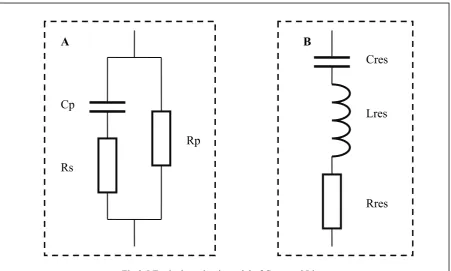
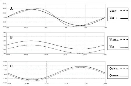
The simulation of the equivalent circuit is done with Cadence. The result can be seen in figure (2.8) and in appendix V. On the left vertical axe the impedance of the piezo element is shown in dBΩ. The right vertical scale shows the phase characteristics of the piezoelectric element.
The impedance curve of the equivalent circuit model shows a similar as the curve of the refer-ence measurement. The biggest differrefer-ence between the circuit model and the referrefer-ence is mainly caused by the lack of the last two resonance frequencies and the value of the resistors in the resonance branches. The shape of the impedance curve shows a capacitive behaviour for the lower frequencies and resistance behaviour for the higher frequencies. The impedance value at 200 Hz is around 71 dBΩ. This is obvious because the same value for the capacitance was used which was calculated for the mathematical model. The capacitance used in the cir-cuit model is therefore close to the capacitance of the measured reference piezo-panel. With the correct values, the equivalent circuit model can be used for simulations. The imped-ance behaviour of the model is the same as for the reference measurement.
2.5 Summary Piezo-panel
In this chapter the piezoelectric theory is discussed. This theory has been used to get some understanding in the electric behaviour of the piezo-panel.
Two models have been formed to predict the behaviour of the piezo-panel. The first model, mathematical model, predicts the impedance behaviour based on material constants. The sec-ond model can be used for circuit simulations. This model uses calculated values from the mathematical model. Comparison with a reference measurement shows that both models show similar frequency response for the impedance and phase characteristics.
3. Functional design
The problems of hysteresis and resonance have been discussed in chapter one and two have to be solved in the system design. Different functional designs are researched in this chapter to find the best or most fitting solution for the problems. The research results in a system which can operate within the given specifications and compensates for the problems. In chapter two the requirements and demands of the system have been discussed. Chapter one and two form the guideline for the research and the design of the functional design. This chapter discusses the functional design, the research of the design and the steps which were made along the way.
3.1 Main function
In chapter two the first major choice for the main system design was already made. The re-quirement to form a complete system where the piezo driver system has to be attached to the panel plus the maximum thickness of the piezo-panel leads to choice to integrate the system on chip. This choice however gives an extra criterion for the design of the system. For exam-ple the maximum capacitance which can be used will be around 10 pF. Some of the imexam-ple- imple-mentation problems can be solved by placing components with excessive values outside the IC. However the intention is to keep the amount of components on the panel as small as pos-sible.
The piezo driver system is needed because the signal system of TNO can not provide the volt-age and current to drive the piezo-panel. An output voltvolt-age of 60 volts is needed with a cur-rent of almost 100 mA. The high output voltage level requires the use of a process technology which can handle the high and low voltages. The silicon-on-insulator (SOI)-based technology called A-BCD is used for the IC design. In this technology transistors are available called DMOST which can withstand the required voltages. This way a 60 volt output stage can be realized.
The input voltage of the piezo driver is 1 Volt and the piezo drive system has to deliver an output voltage of 60 Volt. In other words this requires the use of an amplifier. The main func-tion of the piezo driver will therefore be a power amplifier. Several power amplifier designs exist, each with there own advantages and disadvantages. In this assignment the class-A, class-B, class-AB and class-D amplifier are investigated. Beside the amplifier topologies a charge pump configuration is also investigated. At the end of this section all the topologies will be compared with each other and the best configuration will be chosen.
The research focuses on two aspects of the amplifier types to find the best choice for the piezo driver system. The greatest difference between the amplifiers can be seen in the power dissi-pation and distortion of the output signal. The human hearing is sensitive to distortion of the sound because of this the distortion should be kept as low as possible. The output signal qual-ity requires a distortion of maximum 3% THD.
be-tween a 10 Watt system and a 1 Watt system is quite a lot, 1800 Watt. This gets worse when more piezo-patches and/or panels are needed. High dissipation is unwanted and just a waste of energy.
The second reason to have a low dissipation is because the system will be integrated on chip. An IC-package is limited in the amount of heat/energy which it can radiate to its environment. If the rate at which energy is dissipated in a device is less than the rate at which it is gener-ated, the temperature of the device must rise. In electronic devices, electrical energy is con-verted to heat energy at a rate given by P =V·I Watt, and temperature rises when this heat energy is not removed at a comparable rate. Since semiconductor material is irreversible dam-aged when subjected to temperatures beyond a certain limit, temperature is the parameter that ultimately limits the amount of power a semiconductor device can handle. A normal value which an IC-package can dissipate is about 1 to 5 Watt.
The radiation of heat can be improved by equipping the IC-packages with heat sinks. These are attached to the package and conduct heat outwards. The piezo-panel plate itself could function as heat sink. This however works only when the plate is made of a material with a low heat resistance. Because the material for the plate is not decided on yet, this solution can-not be used. Equipping the IC-package with a heat sink is also can-not possible. The required maximum thickness of 10 mm for the piezo-panel prohibits the use of heat sinks.
3.1.1 Class-A amplifier
Fig. 3.1 Class-A amplifier circuit.
Class-A amplifiers amplify over the whole of the input cycle such that the output signal is an exact scaled-up replica of the input with no clipping [13]. Figure (3.1) shows a circuit imple-mentation of a class-A amplifier. These amplifiers are the usual means of implementing small-signal amplifiers. They are not
very efficient. This is not a problem for small signals, the waste of power is still extremely small, and can be easily tolerated. Only when output powers with appreciable levels of voltage and current are needed, the class-A be-comes problematic. In case of the piezo driver system this forms a prob-lem. In a class-A circuit, the amplify-ing element is biased such that the device is always conducting to some extent, and is operated over the most linear portion of its characteristic curve. Because the device is always conducting, even if there is no input at all, power is wasted. This is the reason
for its high dissipation. The dissipation of a class-A amplifier is given in formula (3.1). In this formula Vss is taken as –Vdd.
Ibias Vdd
PClass−A=2⋅ ⋅ (3.1)
3.1.2 Class-B amplifier
Class-B amplifiers only amplify half of the input wave cycle. As such they create a large amount of distortion, but their efficiency is greatly improved and is much better than class-A. Class-B has a maximum theoretical efficiency of 78.5% for a resistor as load and sinusoidal input signal [13]. This is because the amplifying element is switched off altogether half of the time, and so cannot dissipate power, see
figure (3.2).
A single class-B element is rarely found in practice. A practical circuit using class-B elements is the complementary pair or "push-pull" arrangement. Here, comple-mentary devices are used to each amplify the opposite halves of the input signal, which is then recombined at the output. This arrangement gives excellent effi-ciency, but can suffer from the drawback that there is a small glitch at the "joins" between the two halves of the signal. This is called crossover distortion. Distortion is unwanted for the piezo driver system. In a normal class-B operation the
com-plementary devices each amplify a half of the voltage input signal. This is however not possi-ble for the piezo driver system. The piezo-panel has a capacitive behaviour for the lower fre-quencies and since the input signal of the piezo driver has a maximum frequency of 500 Hz, the load of the system can be assumed to be a capacitor.
Fig. 3.2 Class B amplifier circuit.
To increase the output voltage, charge should be added to the capacitor. The PMOS, in figure (3.2), needs to conduct the current from Vdd to the output. For the decrease of the output voltage, charge should be removed form the capacitor. The current can flow from the output to Vss when the NMOS is active. Thus for a capacitor as output load the complemen-tary devices each need to conduct a half of the current signal. A capacitor causes a 90° phase shift between the output current and output voltage. This can be seen in figure (3.3). Because of this the voltage over the transistors is doubled when it starts conducting. This leads to an increase in the dissipation.
Fig. 3.3 Output voltage and current with capacitive load.
The dissipation can be calculated using formula (3.2), the derivation of the equation is made in appendix VI. In the derivation the negative supply (Vss) is taken as –Vdd.
In equation (3.2) A is used for the amplitude of the output signal. The maximum dissipation occurs when the output signal is also at maximum, A = Vdd. For the piezo driver system the dissipation with a class-B would be:
Watt
The dissipation of a class-B would be 7.2 W. This is better than the dissipation of a class-A amplifier but at the cost of the output signal quality.
3.1.3 Class-AB amplifier
A solution to the distortion of the class-B amplifier is to bias the devices just on, rather than off altogether when they are not in use. This is called class-AB operation. Each device is op-erated in a non-linear region which is only linear over half the waveform, but still conducts a small amount on the other half. Such a circuit behaves as a class-A amplifier in the region where both devices are in the linear
re-gion, however the circuit cannot strictly be called class A if the signal passes out-side this region, since beyond that point only one device will remain in its linear region and the transients typical of class B operation will occur. The result is that when the two halves are combined, the crossover is greatly minimized or elimi-nated altogether. The distortion is there-fore minimal or not at present at all. However, it is important to note that while the distortion of class-AB is less than class-B, the dissipation of class-AB is greater than class-B.
The dissipation of a class-AB amplifier
can be calculated with formula (3.4). This is for a great part the same equation as for the class-B amplifier. The dissipation of the bias current is added. A class-AB amplifier is in most cases biased at 1% of the peak value of the current [13]. In chapter two the peak current is calculated, in equation (1.2), at 94 mA. A bias current of 1 mA is taken. The total dissipation of class-AB is 7.32 Watt.
Fig 3.4 Class-AB amplifier circuit.
Vdd
3.1.4 Class-D amplifier
A class-D amplifier is a power amplifier where all power devices are operated in on/off mode. These amplifiers use pulse width modulation, pulse density modulation. The input signal is converted to a sequence of pulses whose averaged value is directly proportional to the ampli-tude of the signal at that time. Figure
(3.5) shows a simple representation of a class-D circuit. The frequency of the pulses is typically ten or more times the highest frequency of inter-est in the input signal.
Fig. 3.5 Class-D amplifier circuit.
The output of such an amplifier con-tains unwanted spectral components (i.e. the pulse frequency and its har-monics) that must be removed by a passive filter. For a proper function of the amplifier the filter with a coil is needed. Coils are however not easy to make on an IC, especially for larger inductance values, and can therefore better be placed outside an IC. The resulting filtered signal is then an amplified replica of the input.
The main advantage of a class-D amplifier is low power dissipation. Because the output pulses have fixed amplitude, the switching elements (usually MOSFETs) are switched either on or off, rather than operated in linear mode. This means that very little power is dissipated by the transistors except during the very short interval between the on and off states. The wasted power is low because the instantaneous power dissipated in the transistor is the prod-uct of voltage and current, and one or the other is almost always close to zero. These losses are called the conduction losses. The other form of dissipation in a class-D amplifier is caused by the switching of the transistors.
The output transistor size is chosen to optimize power dissipation over a wide range of signal conditions. Ensuring that the voltage drop over the transistors stays small when conducting large current requires the on resistance of the output transistors to be small (typically 0.1 V to 0.2 V) [14]. But this requires large transistors with significant gate capacitance.
The gate-drive circuitry that switches the capacitance consumes power. This “switching loss” becomes excessive if the capacitance or frequency is too high, so practical upper limits exist. The choice of transistor size is therefore a trade-off between minimizing conduction losses during conduction vs. minimizing switching losses. The total dissipation of a class-D ampli-fier can be calculated with formula (3.6) [15], [16].
The transition losses can be approximated with equation (3.7) [15].
In this formula Vdd represents the supply voltage, IRMS the load current, t1 the off/on transition
time, t2 the on/off transition time and T the switching period. For small transition times the
transition losses will be small.
During the switching of the output stage the drain-source capacitance of the transistors is charged and discharged which causes dissipation. However the drain-source is very small and therefore is the loss due to (dis)charging the drain-source very small. This loss is not consid-ered in the switching losses.
The second switching loss effect is PGD. This loss mechanism is the gate drive loss of the
de-vice. Turning-on or off the MOSFET involves charging or discharging the gatecapacitor. When the voltage across a capacitor is changing, a certain amount of charge has to be trans-ferred. The amount of charge required to change the gate voltage between 0 Volt and the ac-tual gate drive voltage give the loss per switching cycle. The gate drive losses can be calcu-lated using formula (3.8).
The gate-source voltage VGS represents the drive voltage of the transistor, CG the gate capacity
and fPWM the switching frequency of the drive pulses.
The conduction losses are determined by the load current and the on-resistance of the transis-tors. As said, large transistors have a small on-resistance. The conduction losses can be calcu-lated with (3.9).
voltage drop over the transistor. For the calculation of the total dissipation of the class-D the following values are taken:
• Vdd =60V
[17] are typical values for a class-D amplifier. The gate-source voltage (Vgs) and gate capaci-tance (CG) were found in DMOS file and simulation in cadence. For the transition times 25%
is taken from the switch period. The total dissipation of the class-D can now be calculated with formula (3.6).
W
The calculation shows that the class-D amplifier has low power dissipation. The dissipation of class-D depends greatly on the size of the transistors and the switching frequency. The dissi-pation can therefore be larger or smaller with other values. However the taken values for the calculation are realistic and give therefore a realistic approximation of the power dissipation of the class-D amplifier.
The distortion of a class-D can be quite low as well when feedback is applied [14], [15], [17]. Audiophile-grade sound quality with THD < 0.01% is attainable in well-designed closed-loop Class D amplifiers [14].
3.1.5 Charge pump
A charge pump is an electronic circuit that uses capacitors as energy storage elements to cre-ate either a higher or lower voltage power source. Charge pump circuits are capable of high efficiencies, sometimes as high as 90-95% while being electrically simple circuits. This to-pology can also be used for the piezo driver system. The piezo element is than used as the load capacitor. Low dissipation can be achieved in this way.
Charge pumps use some form of switching device(s) to control the connection of voltages to the capacitor. For instance, to generate a higher voltage, the first stage involves the capacitor being connected across a voltage and charged up. In the second stage, the capacitor is discon-nected from the original charging voltage and recondiscon-nected with its negative terminal to the original positive charging voltage. Because the capacitor retains the voltage across it (ignoring leakage effects) the positive terminal voltage is added to the original, effectively doubling the voltage. The charge is used to fill up the load capacitor. The capacitor used as the charge pump is typically known as the "flying capacitor". The pulsing nature of the higher voltage output is typically smoothed by the use of the load capacitor. This is the charge pumping ac-tion, which typically operates at tens of kilohertz to minimize the amount of capacitance re-quired.
In case of the piezo driver system the “flying capacitor” has to be, preferably, integrated on chip. This means that this capacitor can have a maximum capacitance of 10 pF. The capaci-tance of the piezo-patch is 500 nF at maximum. The charge pump switching frequency should be fast enough to produce the desired output signal. The maximum slope of the output signal is calculated with equation (3.11).
s Next step is the calculation of the voltage increase or decrease of the load capacitor. This is referred as the pump voltage in formula (3.12).
mV
The total periods per second can now be calculated with equation (3.13).
A switching frequency of 314 MHz is needed for the charge pump configuration. This is quite high and becomes a little to exotic for the application. A larger flying capacitor can be used outside the chip to reduce the