A Broadband Design of UHF Fractal RFID Tag Antenna
Yan Shi*, Chao Fang, Kang Qi, and Chang-Hong Liang
Abstract—In this paper a broadband radio frequency identification (RFID) tag antenna for the ultrahigh-frequency (UHF) band is designed. The proposed antenna consists of a first-order Hilbert fractal structure and a spiral structure. In order to ensure the conjugate matching between the tag antenna and the electronic chip, a T-matching structure is employed. The interaction between two radiating elements makes the proposed antenna a fractional bandwidth of 20% over the frequency range of 820 MHz–1010 MHz and a small size of 0.2092λ0×0.099λ0. Simulated and measured results validate the good performance of the designed tag antenna.
1. INTRODUCTION
Radio frequency identification (RFID) technology in the ultrahigh-frequency (UHF) band has been increasingly dominant in various ID applications, because in this frequency range a broad detectable range, fast reading speed, and the ability to read multiple objects can be easily achieved. A basic RFID system consists of two main components including a set of remote transponders, known as a tag, and a radio-scanner unit, called a reader. A tag includes an antenna and a microchip transmitter with internal read/write memory. A well designed UHF tag antenna can appreciably help its embedded chip to extract RF power from the reader and thus improve the tag readability. Some efforts have been made to design various RFID tag antennas including covered slot antenna [1], circular patch antenna [2], meander antenna [3], planar inverted F-antenna [4], etc. Besides, the design of the impedance matching between the tag antenna and the chip is crucial to the performance of the RFID tag antennas. Several papers have been published on the impedance matching techniques, for example, slot structure [5], T-matching structure [6], and inductively/capacitively coupled structure [7, 8]. In this paper, a novel structure is proposed for a small-sized UHF tag antenna composed of a first-order Hilbert fractal structure and a spiral structure for a quasi-isotropic radiation pattern and a T-matching structure for a broadband impedance matching with a tag chip. Simulation and measurement results show a wide operating frequency bandwidth (820 MHz–1010 MHz), a quasi-isotropic radiation pattern and a good readable range of the proposed tag antenna.
2. ANTENNA DESIGN
Figure 1 shows the structure of the proposed RFID tag antenna. The tag antenna is printed on a FR4 substrate (εr = 4.4 and tanδ = 0.02) with a thickness of 0.5 mm. The tag antenna comprises a first-order Hilbert fractal structure and a spiral structure. The Hilbert fractal structure can realize the size-reducing feature, due to its self-similarity and space-filling nature. It amounts to 0.0793λ0×0.061λ0, which λ0 is the wavelength in free space at the center frequency of 915 MHz. The spiral structure is designed to generate an operating frequency close to the resonant frequency of the Hilbert fractal structure to widen the frequency band. By adjusting the dimensions of the T-matching structure,
Received 4 October 2015, Accepted 8 December 2015, Scheduled 21 December 2015
* Corresponding author: Yan Shi (shiyan@mail.xidian.edu.cn).
q p g W L o n m j i k d e f d c a b r s u v t x y z h Chip
T-match structure Hilbert fractal structure
Spiral structure
Figure 1. Geometry of the proposed RFID antenna.
-30 -27 -24 -21 -18 -15 -12 -9 -6 -3 0
Power reflection coefficient (dB) -15
-12 -9 -6 -3 0
Power Reflection Coefficient (dB)
-24 -21 -18 -15 -12 -9 -6 -3 0
Power Reflection Coefficient (dB) -21
-18 -15 -12 -9 -6 -3 0
Power Reflection Coefficient (dB)
0.6 0.8 1.0 1.2 Frequency (GHz)
(a) (b)
(c) (d)
0.8 1.0 1.2
0.7 0.9 1.1
Frequency (GHz)
0.8 1.0 1.2
0.7 0.9 1.1
Frequency (GHz)
0.8 1.0 1.2
0.7 0.9 1.1
Frequency (GHz)
c=10 mm
c=11 mm
c=12 mm
c=9 mm
c=9.6 mm
d=5 mm
d=6 mm
d=7 mm
d=3 mm
d=4 mm
e=4 mm
e=5 mm
e=2mm
e=3 mm
f=3 mm
f=3.5 mm
f=4 mm
f=2 mm
f=2.5 mm
the input impedance of the tag antenna can be the complex conjugate impedance of the commercial chip Higgs-2, e.g., 17−j120 Ω at 925 MHz. The power reflection coefficient is adapted to deal with the complex impedance of the tag antenna and the chip. The power reflection coefficient denotes as follows [9]:
Power Reflection Coefficient = Zin−Z ∗ chip Zin+Zchip
(1)
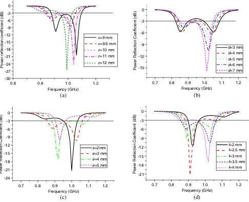
Figure 2 shows the effect of the geometry of the T-matching structure on the power reflection coefficient. It can be seen that there are two resonant frequency bands caused by the Hilbert fractal structure and the spiral structure. The T-matching structure can boost the inductance of the Hilbert fractal and the spiral structure to match with the tag chip and it also broadens the bandwidth. With the decrease of lengthcand the increase of widthdin the T-matching structure, two resonant frequency bands close to each other, thus widening the operating frequency band. In addition, when widthedecreases and length
f increases in the T-matching structure, the first resonance weakens and the second one strengthens. For f = 3.5 mm, and e= 3 mm, two resonances can overlap to broaden the operating frequency band. The optimal dimensions of the proposed tag antenna are shown in Table 1. The whole dimension of the proposed antenna is 68.6 mm×32.5 mm, which corresponds to 0.2092λ0×0.099λ0.
Table 1. Geometric parameters for the proposed tag antenna (unit: mm).
L W a b c d e f g
70 33.5 1.5 1.4 9.6 7 3 3.5 1
h i j k m n o p q
6 4 6 4 5 11 5 3 20
r s t u v x y z
4 9 10 8 7 5 4 3
3. RESULTS AND DISCUSSIONS
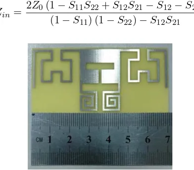
The proposed tag antenna is fabricated and studied, as shown in Fig. 3. Fig. 4 shows the measured input impedance and power reflection coefficient, which are in a good agreement with the simulated results. We can observe that the measured input impedance of the tag antenna is 9.2+j122 Ω at 925 MHz, which is approximately equal to the complex conjugate impedance of the commercial chip Higgs-2. Noted that in the measurement of the input impedance, the tag antenna is considered as a two-port network, and the impedance of the antenna is characterized usingS-parameters [10] as follows:
Zin= 2Z0(1−S11S22+S12S21−S12−S21) (1−S11) (1−S22)−S12S21
(2)
0 50 100 150 200 250
Input impedance (
Ω
)
(a) (b)
0.85 1.00 1.10 0.80 0.90 1.05
Frequency (GHz)
0.95 0.80 0.85 0.90 1.00 1.05 1.10 Frequency (GHz)
0.95 3
0 -3 -6 -9 -12 -15 -18 -21 -24 -27 -30 -33
Power Reflection Coefficient (dB)
simulated real part simulated imaginary part measured real part measured imaginary part
simulation measurement
Figure 4. Measured parameters of the fabricated tag antenna: (a) input impedance, (b) power reflection coefficient.
Figure 5. A fabricated fixture connecting the tag antenna to the network analyzer.
15
10
5
0
15
10
5
0
850 MHz 925 MHz 980 MHz
15
10
5
0
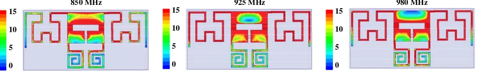
Figure 6. Simulated surface current distributions on the surface of the proposed antenna.
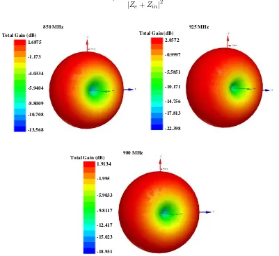
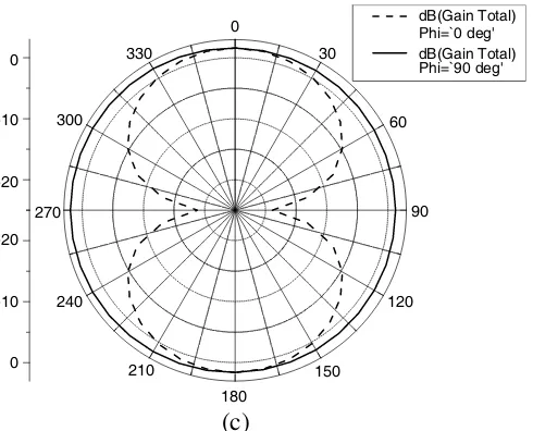
where Z0 is the characteristic impedance of the connected fixture. The fabricated fixture connecting the proposed tag antenna to Agilent 8719ES vector network analyzer is shown in Fig. 5. Generally, 3-dB variations in either chip sensitivity or impedance matching can change the tag range by about 40% [11]. It can be seen from Fig. 4 that the measured half power bandwidth (−3 dB) [12] is 20% from 820 MHz–1010 MHz, a 190 MHz bandwidth. To verify the resonance modes of the proposed antenna, a finite element solver Ansys HFSS is used to simulate surface current distributions on the proposed antenna at 850 MHz, 925 MHz, and 980 MHz, as shown in Fig. 6. Across the operating frequency band, the Hilbert fractal structure and the spiral structure are excited simultaneously to produce two resonant modes close to each other. Fig. 7 shows the three-dimensional simulated radiation patterns at 850 MHz, 925 MHz, and 980 MHz, respectively. Fig. 8 shows the simulated normalizedE-plane andH -plane radiation patterns at corresponding frequencies. According to Figs. 7 and 8, the omnidirectional patterns can be observed. Further, the read range can be estimated by using the Friis free-space formula as [13]
r= λ
4π
PtGtGrτ
wherePt is the power transmitted by the reader,Gt the gain of the transmitting antenna, Gr the gain of the receiving tag antenna, Pth the minimum threshold power necessary to provide enough power to the RFID tag chip, λthe wavelength, andτ the power transmission coefficient given by
τ = 4RcRin
|Zc+Zin|2 (4)
850 MHz 925 MHz
980 MHz
Total Gain (dB) Total Gain (dB)
Total Gain (dB) 1.6875
-1.173
-4.0334
-5.9404
-8.8009
-10.708
-13.568
2.0572
-0.9997
-5.5851
-10.171
-14.756
-17.813
-22.398
1.9134
-1.995
-5.9033
-9.8117
-12.417
-15.023
-18.931
Figure 7. Simulated radiation patterns of the proposed tag antenna.
-15 -10 -5 0
0
30
60
90
150 180
240 270
300 330
-15
-10
-5
0
(a) (b)
120
210
0
30
60
90
150 180
240 270
300 330
120
210 -20
-20 -10 0
-10
0 dB(Gain Total)
Phi=`0 deg' dB(Gain Total) Phi=`90 deg'
(c)
dB(Gain Total) Phi=`0 deg' dB(Gain Total) Phi=`90 deg' 0
30
60
90
150
180 240
270 300
330
120
210 -20
-20 -10 0
-10
0
Figure 8. Simulated normalized radiation pattern: (a) 850 MHz; (b) 925 MHz; (c) 980 MHz.
At 925 MHz, the proposed tag antenna has Gr = 2.06 dB, τ = 0.675, and λ= 0.324 m. Assuming that
Pth =−14 dBm = 0.0398 mW, Pt= 4 W, and Gt = 1 dB, we have the read ranger = 9.55 m.
4. CONCLUSION
This paper proposes a broadband design of the RFID tag antenna consisting of the Hilbert fractal structure and the spiral structure. With a T-matching structure, the tag antenna has an approximately complex conjugate impedance of the commercial chip Higgs-2 over 820 MHz–1010 MHz. The proposed tag antenna is of a small size, i.e., 0.2092λ0×0.099λ0. A prototype of the RFID tag antenna has been fabricated, and simulated and measured results show good performance of the proposed tag antenna.
ACKNOWLEDGMENT
This work was supported by the Natural Science Basic Research Plan in Shaanxi Province of China (No. BD11015020008), Technology Innovation Research Project of the CETC, and Fundamental Research Funds for the Central Universities (No. SPSZ031410).
REFERENCES
1. Chen, S.-Y. and P. Hsu, “CPW-fed folded-slot antenna for 5.8 GHz RFID tags,” Electron. Lett., Vol. 24, 1516–1517, 2004.
2. Padhi, S. K., N. C. Karmakar, C. L. Law, and S. Aditya, “A dual polarized aperture coupled circular patch antenna using a C-shaped coupling slot,” IEEE Trans. Antennas Propag., Vol. 51, 3295–3298, 2003.
3. Marrocco, G., “Gain-optimized self-resonant meander line antennas for RFID applications,” IEEE Antennas Wireless Propag. Lett., Vol. 2, 302–305, 2003.
4. Hirvonen, M., P. Pursula, K. Jaakkola, and K. Laukkanen, “Planar inverted-F antenna for radio frequency identification,”Electron. Lett., Vol. 40, 848–850, 2004.
5. Marrocco, G., “The art of UHF RFID antenna design: Impedance-matching and size-reduction techniques,” IEEE Antennas Propag. Mag., Vol. 50, 66–79, 2008.
7. Son, H.-W. and C.-S. Pyo, “Design of RFID tag antennas using an inductively coupled feed,”
Electron. Lett., Vol. 41, 994–996, 2005.
8. Chang, C. C. and Y. C. Lo, “Broadband RFID tag antenna with capacitively coupled structure,”
Electron. Lett., Vol. 42, 1322–1323, 2006.
9. Perret, E., S. Tedjini, and R. S. Nair, “Design of antennas for UHF RFID tags,” Proceedings of the IEEE, Vol. 100, 2330–2340, 2012.
10. Qing, X., C. K. Goh, and Z. N. Chen, “Impedance characterization of RFID tag antennas and application in tag co-design,”IEEE Trans. Microw. Theory Tech., Vol. 57, 1268–1274, 2009. 11. Nikitin, P. V., K. V. S. Rao, R. Martinez, and S. F. Lam, “Sensitivity and impedance measurements
of UHF RFID chips,”IEEE Trans. Microw. Theory Tech., Vol. 57, 1297–1302, 2009.
12. Rajagopalan, H. and Y. Rahmat-Samii, “A novel conformal all-surface mount RFID tag antenna design,”Proceedings of the IEEE Antenna and Propagation Society International Symposium, 1–4, 2009.