Digit-Level Serial-In Parallel-Out Multiplier Using Brent
Kung Adder
Veduruparthi Bala Naga Jyothi & Dr. K. Amit Bindaj
1
M.Tech scholar, Dept of E.C.E, Sai Tirumala NVR Engineering College, Narasaraopet.
2Professor & H.O.D. Dept of E.C.E, Sai Tirumala NVR Engineering College, Narasaraopet.
ABSTRACT: Adders are the most essential part of any digital system. Providing an efficient adder design satisfies the tradeoff between speed and space aides in increasing the performance of the system. In the modern age in addition to the tradeoff among speed and space, power consumption plays a vital role. Devices with low power consumption and good performance are always preferred. Parallel Prefix adders are the ones which are widely used in Digital Design. This is primarily because of the flexibility in designing the Adders. Brent Kung Adder is a low power adder, as it utilizes the minimum circuitry to obtain the result. The 16 bit design is extended to 32 bit, implemented in the physical level and successfully simulated.
Index Terms—Digit-level architecture, finite field arithmetic, multiplication algorithm, redundant representation.
I.INTRODUCTION
Finite field computation has recently gained growing attention due to its wide range of applications in coding theory, error control coding, and especially in cryptography, where ElGamal and elliptic curve cryptography (ECC) two out of the three well-known cryptosystems, are based on finite field arithmetic. Finite field computation is performed using arithmetic operations in the underlying finite field. Among the basic field operations, multiplication plays a fundamental role as more complicated operations, namely, field exponentiation and field inversion can be carried out with consecutive use of field multiplication.
Similar to linear algebra, the concept of representation bases is also used in finite field arithmetic to represent field elements. The choice of representation system mainly affected by the hardware in use and the requirements of the cryptosystem, has a great impact on computational performance. A few number of representation systems for extension binary fields have been proposed in the literature, such as polynomial basis normal basis (NB), redundant basis (RB), and dual basis. In both normal basis (NB) and redundant representation (RB), squaring operation can be performed by applying a simple permutation operation on the coordinates. This makes them high efficient for the hardware implementations of cryptographic algorithms which utilize frequent squaring or exponentiation, like point addition/doubling in ECC. Moreover, redundant representation is of a special interest because of its unique feature in accommodating ring type operations. This not only offers almost cost-free squaring operation but also eliminates the need for modular reduction in multiplication.
II.EXISTED SYSTEM
1
)/
2
)
identical modules shown inside the dashed
boxes.
Fig. 1.Existed architecture for digit-Level SIPO RB multiplier
At the bottom, there is a network of XOR gates
adding 2
w
outputs of each module together to
form output coordinates. Each module is made
of a layer of 2
w
AND gates receiving the outputs
of the wire expansion module as their first input
set. The second input set is received from certain
bits of operand
A
in a digit-serial fashion. Each
AND gate is followed by an XOR gate
connected immediately to a flip-flop.
The output of the flip-flop is fed back to the
XOR gate forming an accumulation unit
together. Two AND gates along with their
respective accumulation units form a structure
responsible to realize the operations. One of
these structures is shown in the Fig. 1 inside a
dotted block for
j
= 0 and
k
= 0. In total, the
architecture contains
w(n
− 1
/
2
)
such structures,
each of which consists of two AND gates, two
XOR gates, and two flip-flops to generate and
store each clock cycle.
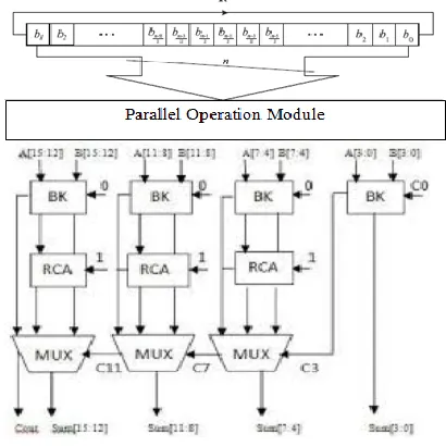
III.PROPOSED SYSTEM
Brent-Kung adder is a very popular and most
widely used adder. Generally, it gives an
excellent number of stages from input to all
outputs but with
asymmetric loading ofIntermediate stages. It is one of the parallel prefix adders.
Fig 2. Proposed block diagram
It is one of the parallel prefix adders where these
adders are the ultimate class of adders that are
depends on the usage of generate and propagate
signals. In case of Brent kung adders along with
the cost, the wiring complexity is also less. But
the gate level depth of Brent-Kung adders is 0
(log2 (n)).
In ripple carry adders each bit have to wait for
the last bit operation. In parallel prefix adders
instead of waiting for the carry propagation of
the first addition, the idea here is to overlap the
carry propagation of the first addition with the
computation in the second addition, and so forth,
since repetitive additions will be performed by a
multi-operand adder.
The construction of efficient Brent kung adder
consists of three stages. They are pre-processing
stage, carry generation stage, post-processing
stage.
In the pre-processing stage, generate and propagate are from each pair of inputs. The propagate perform “XOR” operation of input bits and generate operation “AND” operation of input bits. The propagate (Pi) and generate (Gi) are shown in below equations 1 and 2.
(1)
(2) B. Carry Generation Stage
In this stage, carry is generated for each bit called as carry generate (Cg). The carry propagate and carry generate is generated for the further operation but final cell present in the each bit operation gives carry. The last bit carry will help to produce sum of the next bit simultaneously till the last bit. The carry generate and carry propagate are given in below equations 3 and 4.
(3)
(4) The above carry propagate Cp and carry generation Cg in equations 3 & 4 is black cell and the below shown carry generation in equation 5 is gray cell. The carry propagate is generated for the further operation but final cell present in the each bit operation gives carry. The last bit carry will help to produce sum of the next bit simultaneously till the last bit. This carry is used for the next bit sum operation, the carry generate is given in below equations 5.
(5) C. Post-processing stage
It is the final stage of an efficient Brent Kung adder, the carry of a first bit is XORed with the next bit of
propagates then the output is given as sum and it is shown in equation 6.
(6) It is utilized for two sixteen bit addition operations and each bit carry is undergoes post-processing stage with propagate and produce the final sum. The first input bits goes under pre-processing stage and it will produce propagate and generate. These propagates and generates undergoes carry generation stage which produces carry generates and carry propagates, these undergoes post-processing stage and provides final sum.
In Efficient Brent Kung adder, black cell operates three gates and gray cell operates two gates. The gray cell will reduce the delay and memory because it operates only two gates. The proposed adder is design with the both black and gray cells. By using gray cell operations at the last stage of proposed adder gives a enormous dropping delay and memory used.
The proposed adder is shown in fig 3 which increases the speed and decreases the memory for the operation of 8-bit addition. The input bits Ai and Bi concentrates on generate and propagate by XOR and AND operations. These propagates and generates undergoes the operations of black cell and gray cell and provides the carry Ci. That carry is XORed with the propagate of next bit, that gives sum.
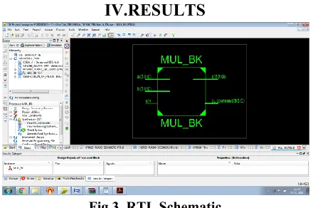
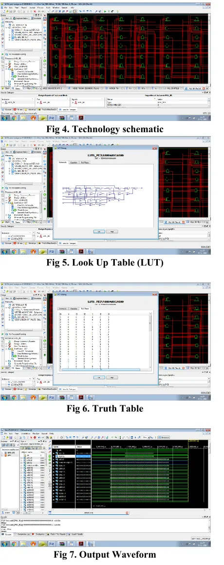
IV.RESULTS
Fig 4. Technology schematic
Fig 5. Look Up Table (LUT)
Fig 6. Truth Table
Fig 7. Output Waveform
V.CONCLUSION
In this paper, a new approach is implemented to
design a digital level Serial-In Parallel Out
multiplier
using
Parallel
Adder
which
concentrates on gate levels to improve the speed
and decreases the memory. In this case, a
specific feature of redundant representation was
used to alleviate the redundancy problem in this
representation system. It is like tree structure and
cells in the carry generation stage are minimized
to speed up the binary addition. The proposed
adder addition operation provides great
advantage in reducing delay.
VI.REFERENCES
[1] T. ElGamal, “A public key cryptosystem and a signature scheme based on discrete logarithms,” IEEE Trans. Inf. Theory, vol. 31, no. 4, pp. 469–472, Sep. 2006.
[2] I. F.Blake, G. Seroussi, and N. P. Smart, Elliptic
Curves in Cryptography (London Mathematical
Society Lecture Note Series). Cambridge, U.K.: Cambridge Univ. Press, 1999.
[3] A. J. Memezes, P. C. Van Oorschot, and S. A. Vanstone, Handbook of Applied Cryptography (Discrete Mathematics and Its Applications). Boca Raton, FL, USA: CRC Press, 1996.
[4] T. Itoh and S. Tsujii, “A fast algorithm for computing multiplicative inverses in GF(2m) using normal basis,” Inf. Comput., vol. 78, no. 3, pp. 171– 177, 1988.
[5] C. Rebeiro, S. Roy, D. Reddy, and D. Mukhopadhyay, “Revisiting the Itoh–Tsujii inversion algorithm for FPGA platforms,” IEEE Trans. Very Large Scale Integr. (VLSI) Syst., vol. 19, no. 8, pp. 1508–1512, Aug. 2011.
[7] J. Omura and J. Massey, “Computational method and apparatus for finite field arithmetic,” U.S. Patent 4 587 627, May 6, 1986.
[8] S. G. Smith, and P. B. Denyer, Serial Data Computation, Kluwer, 1988.
[9] R. I. Hartley, and K. K. Parhi, Digit-Serial Computation, Kluwer, 1995.
[10] Y. N Chang, J. H. Satyanarayana, and K. K. Parhi, “Systematic design of high-speed and low-power digit-serial multipliers,” IEEE Trans. on Circuits Syst.-II, vol. 45, No. 12, pp. 1585-1596, Dec. 1998.
[11] O. Gustafsson, and L. Wanhammar, “Bit-level pipelinable general and fixed coefficient digit-serial/parallel multipliers based on shiftaccumulation,” in IEEE Conf. Proc. of Electr. Circuits & Syst. 2002, vol. 2, pp. 493-496. Sept., 2002.
[12] O. Nibouche, and M. Nibouche, “On designing digit multipliers,” in IEEE Conf. Proc. of Electr. Circuits & Syst. 2002, vol. 3, pp. 951-954. Sept., 2002.
[13] A. Avizienis, “Signed-digit number representation for fast parallel arithmetic,” IRE Trans. Electronic Comp., vol. 10, pp. 389-400, 1961. [14] M. Karlsson, M. Vesterbacka, and W. Kulesza, “A method for increasing the throughput of fixed coefficient digit-serial/parallel multipliers,” in IEEE Proc. of Int. Symp. on Circuits and Systems, ISCAS'04, vol. 2, pp. 425-428, Vancouver, Canada, May 23-26, 2004.
[15] M. Renfors, Y. Neuvo, “The maximum sampling rate of digital filters under hardware speed constraints,” IEEE Trans. on Circuits and Systems, Vol. 28, No. 3, pp. 196-202, March, 1981.
[16] M. Karlsson, M. Vesterbacka, and W. Kulesza, “Ripple-carry versus carry-look-ahead digit-serial adders,” in Proc. IEEE Conf. NORCHIP'03, pp. 264-267, Riga, Latvia, Nov., 2003.
[17] L. Wanhammar, DSP Integrated Circuits, Academic Press, 1999.
[18] O. Gustafsson, and L. Wanhammar, “Optimal logic level pipelining for digit-serial implementation
of maximally fast recursive digital filters”, in Proc. RVK-02, Karlskrona, Sweden, 2002.
[19] C. Nagendra, M.J. Irwin, and R. M. Owens, “Area-time-power tradeoffs in parallel adders,” IEEE Trans. on Circuits & Syst. II, vol. 43. No. 10, pp 689-702. Oct. 1996.
[20] R. P. Brent, and H. T. Kung, “A regular layout for parallel adders,” IEEE Trans. on Comput., vol. 31, pp. 260-264, March., 1982.
Dr K AMIT BINDAJ, PhD from Jodhpur National University, Jodhpur, Recg. by Govt. of Rajasthan. Presently working as H.O.D. and Dean R &D , ECE in Sai Tirumala NVR Engineering college , Narasaraopeta, having a Teaching experience of almost 14 years. His area of research is emerging Wireless communication Technology, 4G Long Term Evaluations(LTE-A) and also ICT enabled services. He has also attended and conducted about dozen of workshops and FDP. He presented & published the Research Papers in almost more than dozen of National and International conferences and High impact factor International Journals.
VEDURUPARTHI. BALA