ABSTRACT
KAMAT, PRATHAMESH SHIVANAND. Energy Storage Integration in Stand Alone Wave Energy Conversion System. (Under the direction of Dr. Subhashish Bhattacharya.)
©Copyright 2016 by Prathamesh Shivanand Kamat
Energy Storage Integration in Stand Alone Wave Energy Conversion System
by
Prathamesh Shivanand Kamat
A thesis submitted to the Graduate Faculty of North Carolina State University
in partial fulfillment of the requirements for the Degree of
Master of Science
Electrical Engineering
Raleigh, North Carolina
2016
APPROVED BY:
Dr. David Lubkeman Dr. Mesut Baran
DEDICATION
BIOGRAPHY
Prathamesh Kamat was born on October 17, 1990 in Mumbai (Maharashtra), India. He did his schooling from VPM Vidya Mandir, Dahisar, Mumbai. He graduated from Sardar Patel College of Engineering, Mumbai with a Bachelor in Electrical Engineering in 2012. Prathamesh was an Executive Engineer in Air Insulated Switchgear (AIS) Medium Voltage (MV) Business Unit at Siemens India from 2012-2014. He worked on research and development department for design modifications of MV Vacuum Circuit Breakers at Siemens. Many of his responsibilities included the design to order and development of the product based on site complaints.
ACKNOWLEDGEMENTS
I am sincerely thankful to my advisor, Dr. Subhashish Bhattacharya for the guidance he has provided me during my graduate program at North Carolina State University. Dr. Bhattacharya has been always helpful and he gave me excellent opportunity to work on wave energy generation and control project.
I thank Dr. David Lubkeman for accepting to become a member of the committee. I am thankful all the help and guidance in the coursework which motivated me in my thesis.
I thank Dr. Mesut Baran for accepting to become a member of the committee. I am thankful for your valuable advice and teaching.
I thank Samir Hazra for his excellent mentorship throughout my masters program. You gave me wonderful opportunity to apply the knowledge of power electronics by making me involved in various kinds of hardware as well as software tasks in your project. Those inspired me to learn power electronics in depth and also enhanced my skills. The knowledge needed for executing this thesis work wouldn’t have been possible without your guidance and support.
I thank FREEDM Systems Center for sharing the resources for this project.
I thank ABB for providing funding and for an opportunity to develop the hardware and use it as a part of this thesis.
I thank Swaroop Mohapatra for motivating me in my tough times and helping me to achieve my thesis successfully.
I thank Ashish Shrivastav for his support, suggestions and support throughout the project work and coursework. I also appreciate the valuable suggestions from seniors and friends, Ankan De, Sachin Madhusudan, Krishna Mainali, Awneesh Tripathi, Ritwik Chattopadhyay, Kasu Naidu, Anirudha Mahajan, Abhay Negi, Akshat Yadav and Ganapati Pai at FREEDM Systems Center.
I extend my gratitude towards Karen Autry for always cheering me up.
I thank Hulgize Kassa for his help with electrical equipment as well as supervision assuring my safety in the laboratory.
I thank Anish, Rohit, Ameya, Pratik, Yaman, Ronak, Nivedhitha, Vaishnavi, Ashish Sub-ramnium, Wasim, Utkarsh, Ayush for their support and contribution in my learning.
TABLE OF CONTENTS
LIST OF TABLES . . . vii
LIST OF FIGURES . . . .viii
Chapter 1 Introduction . . . 1
Chapter 2 System Architecture . . . 5
Chapter 3 Control and Simulation . . . 8
3.1 Model and Controller Design . . . 9
3.1.1 ESS Current Controller Design . . . 9
3.1.2 ESS Voltage Controller Design . . . 10
3.1.3 Rectified Current Controller Design . . . 12
3.2 Simulation Results . . . 13
3.2.1 ESS Current Control Model . . . 13
3.2.2 ESS Voltage Control Model . . . 15
3.2.3 Rectified Current Control Model . . . 16
3.2.4 System Model With Voltage Source as ESS . . . 19
Chapter 4 Hardware Implementation . . . 20
4.1 Hardware Setup . . . 20
4.2 Experimental Investigation . . . 23
4.2.1 ESS Current Controller Test . . . 23
4.2.2 ESS Voltage Controller Test . . . 24
4.2.3 Rectifier Current Controller Test . . . 24
4.2.4 PMSG operation using ABB ACS800 drive . . . 26
4.2.5 System Setup With DC Supply as ESS . . . 27
4.2.6 Self excitation for PMSG . . . 27
4.2.7 Real time simulation using NI Labview and CompactRIO . . . 29
Chapter 5 Hybrid Energy Storage . . . 30
5.1 Supercapacitor . . . 30
5.2 Supercapacitor charging and discharging . . . 31
5.2.1 Constant Current Constant Voltage control . . . 31
5.2.2 Simulation result for charging and discharging of supercapacitor . . . 33
5.2.3 Hardware results for charging and discharging of supercapacitor . . . 34
5.3 System with supercapacitor . . . 34
5.3.1 Simulation Results for System with Supercapacitor . . . 34
5.3.2 System model hardware implementation using supercapacitor . . . 36
5.4 Hybrid energy storage . . . 36
5.4.1 Difference between supercapacitor and battery . . . 36
5.4.3 Control and simulation of battery current . . . 38 5.4.4 System model simulation of hybrid supercapacitor and battery control . . 41 5.4.5 System model hardware implementation using hybrid supercapacitor and
battery control . . . 43 5.5 Conclusion . . . 45
LIST OF TABLES
Table 4.1 System parameters . . . 21 Table 4.2 Voltage Compensation of PMSG using self-excitation capacitors . . . 28
LIST OF FIGURES
Figure 1.1 Schematic of the emulating system . . . 2
Figure 1.2 Hardware setup for emulating WEC . . . 2
Figure 1.3 Sinusoidal speed reference and PMSG terminal voltage . . . 3
Figure 1.4 Wave energy generation for grid application . . . 3
Figure 1.5 Wave energy generation for stand-alone application . . . 4
Figure 2.1 System Block Diagram . . . 5
Figure 2.2 System control structure . . . 6
Figure 3.1 System power circuit with ESS . . . 9
Figure 3.2 Iess control bode plot . . . 10
Figure 3.3 Vdc control bode plot . . . 11
Figure 3.4 Irect control bode plot . . . 12
Figure 3.5 Model for ESS current controller test . . . 13
Figure 3.6 ESS current controller . . . 14
Figure 3.7 ESS current plot . . . 14
Figure 3.8 Model for ESS voltage controller test . . . 15
Figure 3.9 ESS voltage controller . . . 15
Figure 3.10 ESS current plot . . . 16
Figure 3.11 DC bus voltage plot . . . 16
Figure 3.12 Model for rectifier current controller test . . . 17
Figure 3.13 Rectifier current controller . . . 17
Figure 3.14 Rectified currentirect plot . . . 18
Figure 3.15 System model with voltage source as ESS . . . 19
Figure 3.16 VDC plot from system model simulation . . . 19
Figure 4.1 System Hardware . . . 22
Figure 4.2 iesscontroller test in hardware . . . 23
Figure 4.3 iesscontroller test in hardware plots . . . 24
Figure 4.4 VDCcontroller test in hardware Ch1: DC Bus VoltageVDC controlled at 50V, Ch2: Reference currentiessref (A), Ch3: Measured inductor current iess(A) . 25 Figure 4.5 iGEN controller test in hardware Ch1: Actual inductor currentirect(A), Ch2: Reference currentirectref (A), Ch3: Measured inductor currentirect (A) . . . 25
Figure 4.6 PMSG terminal voltage and speed reference, Ch1: Stator line voltage Vab (Scale 1V=3V), Ch2: Rectified voltage Vrect (1V), Ch1: Stator line voltage Vbc (Scale 1V=3V) . . . 26
Figure 4.7 System with ESS test in hardware Ch1: DC Bus Voltage VDC controlled at 50V, Ch2: Supercapacitor boost inductor currentiSC (A), Ch3: Rectifier boost inductor currentiRect(A) . . . 27
Figure 4.8 Self-excitation capacitor connection for PMSG . . . 28
Figure 4.9 Buoy CRIO model in NI Labview . . . 29
Figure 5.1 Maxwell 48V supercapacitor module . . . 31
Figure 5.2 Vsc control bode plot . . . 32
Figure 5.3 Supercapacitor charging schematic . . . 33
Figure 5.4 Constant current and constant voltage logic . . . 34
Figure 5.5 Plots for system model with supercapacitor of 30V . . . 35
Figure 5.6 Supercapacitor charging-discharging test in hardware Ch1: Supercapacitor Voltage VSC controlled at 10V, Ch2: SC boost inductor reference current iSCref (A), Ch3: SC boost inductor currentiSC (A) . . . 36
Figure 5.7 System with supercapacitor test in hardware Ch1: SC boost inductor current iSC (1V=1A), Ch1: Ch2: Rectifier boost inductor current iRect (1V=1A), Ch3: DC Bus Voltage VDC (V) . . . 37
Figure 5.8 Ib control bode plot . . . 39
Figure 5.9 vsc control bode plot . . . 40
Figure 5.10 System circuit with hybrid battery and supercapacitor . . . 41
Figure 5.11 Plots for system model with hybrid battery and supercapacitor control . . . . 42
Figure 5.12 Hybrid battery and supercapacitor controller . . . 43
Figure 5.13 Hardware setup for wave energy generation with hybrid energy storage . . . 44
Chapter 1
Introduction
Ocean energy is emerging as renewable source of energy which can be used for generation of electricity. It can serve as a cost effective solution for providing power to the navy applications. Compared to solar and wind power generation, ocean wave energy is yet to gain the popularity. But researches are being carried to find efficient and economical solutions for generating power using wave energy.
Several wave energy converter (WEC) designs have been made in order to harvest maxi-mum energy from ocean wave [1]. Out of those, point absorber buoy and paddle based WEC systems drive generator directly to provide power [2]-[4]. By use of efficient WEC, wave energy generated can be used in grid application or stand-alone application.
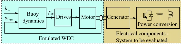
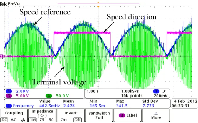
Research also has been done on designing a WEC dynamic model in [16]. In this, WEC mechanism is also emulated based on the dynamic equations. The overall system diagram for emulation is shown in the Fig. 1.1. Ocean wave can be considered as combination of several low frequency sinusoidal waves. Buoy dynamics and wave nature can be emulated using NI labview and real-time simulator CompactRIO to generate necessary torque command signal for drive. Hardware setup can be developed as shown in Fig.1.2 [16]. Sinusoidal speed reference can also be generated by using this setup as shown in Fig. 1.3 [16]. In this thesis, single sinusoidal wave with a period of 10 sec is considered for simplicity. This reference command is given to the drive by DSP using appropriate scale.
Figure 1.1: Schematic of the emulating system
Figure 1.2: Hardware setup for emulating WEC
generate reactive power for the grid if required. Line filters are installed in order to bring down the line current ripple to an acceptable range. A line frequency transformer can interface the whole unit of WECS with the grid. Transformer provides galvanic isolation as well as necessary voltage step up to connect the system with the grid.
Fig. 1.5 shows wave energy generation for grid application [6]. The PMSG which is connected to the WEC generates oscillatory power. PMSG output power is then rectified using AC-DC converter. It is passed through DC-DC boost converter and connected to a stand-alone resistive load. Energy storage system is connected to the load through a bi-directional DC-DC converter.
mi-Figure 1.3: Sinusoidal speed reference and PMSG terminal voltage
Figure 1.4: Wave energy generation for grid application
crogrid system [7], wind energy generation [8] and electric vehicles [9]. Ocean wave is oscillatory in nature and hence generates oscillatory power. To provide constant power to a stand-alone application, it is necessary to filter out the oscillations using Energy Storage System (ESS).
This thesis focuses on the stand-alone wave energy generation. It discusses about the con-troller design, model simulation and hardware development which can be done using minimum components. It also proposes the hybrid energy storage system control for better power smooth-ing. For this purpose; permanent magnet synchronous generator (PMSG), AC Drive, DC-DC power converter, supercapacitor, DC power supply and a stand-alone resistive load bank is used.
Figure 1.5: Wave energy generation for stand-alone application
Chapter 3 explains the system controller design and model simulation. It includes the trans-fer functions, controller parameters and bode plot results to show the approach. It also shows the MATLAB models which verify the controller design by model simulation of system blocks. In this chapter, ESS is considered as a single block which works as a power smoothing device.
Chapter 4 is focused on the hardware development and the experimental results which ver-ify the simulation results obtained in chapter 3. It shows the hardware structure built in lab and elaborates the step by step experimenting process to be carried out as we are building the system.
Chapter 2
System Architecture
Research has been done on wave energy generation for stand-alone application in [6] and similar design approach is used in this thesis. The system design used is as shown in the Chapter 1 Fig. 1.5.
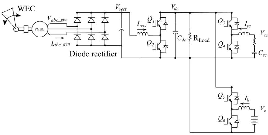
The power circuit used for the system is as shown in Fig. 2.1. The voltage output is rectified by a diode rectifier bridge. Supercapacitor and battery are used as energy storage devices. For maintaining the constant power for stand-alone application, it is necessary to control DC bus voltage and individual powers from generator and energy storage systems. DC bus voltage is regulated by supercapacitor side DC-DC boost converter. Output DC bus voltage is generally controlled at a value higher than the rectified voltage. Another boost converter is used to control the rectified current. This current is controlled to generated optimum power from PMSG. Rec-tifier current reference is generated proportional to the WEC speed reference. This assumption is necessary because output impedance of the system needs to be equal to its source impedance in order to generate optimal power [6].
Thus, overall system control is achieved by controlling the current flow from rectifier, super-capacitor and battery. Supersuper-capacitor boost converter is used to control DC bus voltage and to provide peak power requirement. Battery can charge or discharge with suitable control in order to provide average power mismatch and also limit supercapacitor terminal voltage. This controol strategy will be discussed in later chapters in detail. In any case, ESS power is con-trolled in such a way that load should always get constant power. ESS will charge or discharge whenever generated power is above or below average load power respectively.
Chapter 3
Control and Simulation
Boost converters are designed for 10kHz switching frequency. Maximum DC bus voltage is considered to be 200V. Given ripple in current, inductance can be found as
L= VinDTs
2∆I (3.1)
Consider schematic shown in Fig. 3.1. For ESS side boost converter, considering maximum input voltage of energy storage asVess= 50V and current maximum asI = 20A. Hence for ESS boost converter,Lessis chosen to be 1mH considering 5% current ripple. Similarly; for rectifier boost converter, considering maximum input voltage of rectified voltage as Vrect = 150V and current maximum asI = 10A.Lrect is chosen to be 5mH considering 5% current ripple. Capacitor Cdc can be selected to minimize the ripple in output voltage. In this case, 470µF is chosen.
System control design and the modeling is done using MATLAB. Boost converter can be controlled using numerous methods depending upon the control requirement [10]. For simplicity we will first consider ESS as an ideal energy storage device like a constant DC supply which can charge or discharge as required. In this system, our aim is to control the power flow through the PMSG and charging-discharging of the ESS while maintaining the voltage at the DC bus constant. Hence, normal voltage regulator design for the boost won’t be sufficient since it will fail to control the current flow. It is necessary to operate the converter in current control mode. A simple approach would be to design separate controllers for current as well as voltage. Since PMSG generated terminal voltage is dependent on the speed of the wave, it is fluctuating in nature ranging from zero to the peak value. Hence ESS side boost converter is suitable for regulating the output voltage at the DC bus.
the control of the system. These controllers are as follows.
1. ESS Current Controller
2. ESS Voltage Controller
3. Rectified Current Controller
Figure 3.1: System power circuit with ESS
3.1
Model and Controller Design
3.1.1 ESS Current Controller Design
Consider the Fig.3.1 We can write the voltage across the ESS side inductorLess as
dessVdc−Vess=IessLesss (3.2)
Here Vdc is the output DC voltage which is assumed to be 200V, Iess is the ESS side boost converter inductor current,dessis the duty ratio of the ESS boost. SinceVessis the disturbance input, the transfer function can be given as follows.
GIess(s) =
Iess(s)
dess(s)
= Vdc
Lesss
(3.3)
controller is designed and Kp, Ki values are appropriately chosen to achieve 300Hz bandwidth for current iess.
HIess(s) =
0.00944(s+ 2.966)
s (3.4)
The plant transfer function, controller and closed loop gain bode plot is shown in the Fig. 3.2.
Figure 3.2: Iesscontrol bode plot
3.1.2 ESS Voltage Controller Design
We can write the voltage across the output capacitor Cdc as
Vdc(s) =
Idc(s)
Cdcs
, (3.5)
Vdc(s) =
1−Dess
Cdcs
The transfer function can be given as follows.
GIess(s) =
Vdc(s)
Iessref(s)
= 1−Dess
Cdcs
(3.7)
PI controller is designed and Kp,Ki values are appropriately chosen to achieve 45Hz bandwidth for voltage vdc. In this case bandwidth of voltage controller is chosen lesser than the current controller. Since this is acting like a current mode control, current controller needs to be higher than the voltage controller bandwidth.
HIess(s) =
0.531(s+ 25.02)
s (3.8)
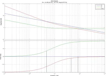
The plant transfer function, controller and closed loop gain bode plot is shown in the Fig. 5.2.
3.1.3 Rectified Current Controller Design
We can write the voltage across the rectifier side inductor Lrect as
drectVdc−Vrect=IrectLrects (3.9)
HereVrect is the diode rectifier output voltage which is dependent on the wave speed reference.
Irect is the PMSG side boost converter inductor current, drect is the duty ratio of the PMSG boost. Since Vrect is the disturbance input, the plant transfer function can be given as follows.
GIrect(s) =
Irect(s)
drect(s)
= Vdc
Lrects
(3.10)
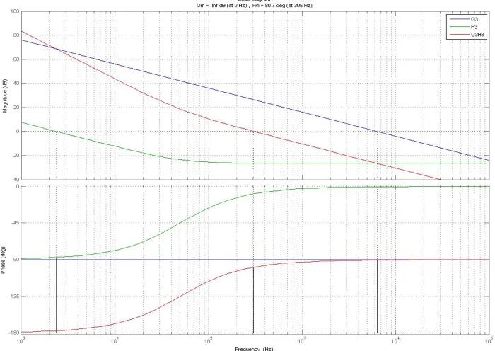
PI controller is designed and Kp, Ki values are appropriately chosen to achieve 300Hz bandwidth for current Irect.
HIrect(s) =
0.0473(s+ 14.86)
s (3.11)
The plant transfer function, controller and closed loop gain bode plot is shown in the Fig. 3.4.
3.2
Simulation Results
The system block diagram shown in the Fig. 3.1 is modeled in the MATLAB Simulink. Basic PMSG mathematical model is used to generate the voltage based on the sinusoidal speed reference. Diode rectifier bridge is used from sympower toolbox. Boost converter models are created using single leg converter Real Time - Event toolbox. Controllers are modeled using MATLAB logic blocks with Kp and Ki values obtained in equations 3.4, 3.8 and 3.11. Following subsections show the simulation of individual boost converters and their controllers to ensure the correct operation. This step by step modeling is started by considering ESS side boost converter.
3.2.1 ESS Current Control Model
Energy storage system can be assumed like a constant DC voltage source as shown in Fig. 3.5. Current controller model is shown in the Fig. 3.6. The DC bus voltage is maintained at 200V by DC supply in order to test the current controller. This controller is suitable for controlling theiess as shown in Fig. 3.7. Current is controlled at 3A as required.
Figure 3.6: ESS current controller
Isc
time(s)
0.00 0.05 0.10 0.15 0.20 0.25 0.30 0.35 0.40 0.45 0.50
Is
c
(A
)
-80 -70 -60 -50 -40 -30 -20 -10 0 10 20
Signal
3.2.2 ESS Voltage Control Model
We need to control the charging and discharging of the ESS while maintaining the voltage at the DC bus constant. In other words, when the generated power is greater than the load, the ESS should be in the charging cycle. When the generated power is less than the load, the ESS should be in the discharging cycle. Hence, voltage controller should be able to decide the reference of the ESS current. This is achieved as shown in the Eqn. 3.7. It will be seen in later chapters that this voltage will actually be controlled by supercapacitor boost converter.
Figure 3.8: Model for ESS voltage controller test
Figure 3.9: ESS voltage controller
Isc
time(s)
0.0 0.5 1.0 1.5 2.0 2.5 3.0 3.5 4.0 4.5 5.0
Is c( A ) 0 1 2 3 4 5 6 7 8 9 10 11 12 13 14 15 16 17 Signal
Figure 3.10: ESS current plot
time (s)
0.0 0.5 1.0 1.5 2.0 2.5 3.0 3.5 4.0 4.5 5.0
V d c (V ) 50 60 70 80 90 100 110 120 130 140 150 160 170 180 190 200 Signal
Figure 3.11: DC bus voltage plot
3.2.3 Rectified Current Control Model
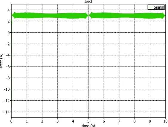
But in this simulation, currrent controller is first test for constant current reference of 3A. It can be modified later to sinusoidal reference once successful operation of controller is achieved. Output DC bus is maintained at 200V using a voltage source as if it is being regulated by ESS side boost converter. This is done to remove the complexity of the models and keep design simple for testing individual controller.
The current controller based on Eqn. 3.10 and Eqn. 3.11 provides the suitable duty cycle to the boost model. Sudden load change from 100Ω to 50Ω at 2.5sec does not affect the stability of the controller and current is regulated at 3A as shown in Fig. 3.14.
Figure 3.12: Model for rectifier current controller test
Fig. 3.13 shows the controller logic. This controller is suitable for controlling the irect as shown in Fig. 3.14. It can be seen from the plot that the current is controlled at 3A as required.
Irect
time (s)
0 1 2 3 4 5 6 7 8 9 10
Ir
e
ct
(
A
)
-14 -12 -10 -8 -6 -4 -2 0 2
4 Signal
3.2.4 System Model With Voltage Source as ESS
By combining models in Fig. 3.15 and Fig. 3.12, system model is created. Vdc is maintained at 200V by ESS boost converter. Current reference for rectifier current controller is generated as a multiple of speed reference. Load current is changed from 2A to 12A and load regulation can be seen in 3.16
Figure 3.15: System model with voltage source as ESS
time (s)
0 1 2 3 4 5 6 7 8 9 10
V
d
c
(V
)
0 20 40 60 80 100 120 140 160 180
200 Signal
Chapter 4
Hardware Implementation
This chapter includes the hardware implementation of the control simulations carried in the Chapter 2. For assuring the system performance, the system is operated with voltage source as ESS.
4.1
Hardware Setup
Hardware setup for the wave energy genearation is shown in Fig. 4.1. Entire setup can be devided into 4 parts.
1. Control circuit
2. Power converter circuit
3. Supercapacitor and battery circuit
4. Motor-generator set
Fig. 4.1a shows the control circuit. Oztek OZDSP3000 control board is used for the entire control in the system. It provides the analog speed reference to the ABB ACS800 drive. It has an important role in sending PWM signals to the power converters. Figure also shows an inter-face board with flat ribbon cables. This board is used as an interinter-face between control board and power converter. It is used to provide fault protection as well as to receive sensor signals from the voltage sensors and current sensors. Power supply with various output voltages such as 5V, 24V, 15V and -15V is used to power the control board, interface board and other requirements in the system.
Table 4.1: System parameters
Component Parameters Value
Voltage (L-L) 460 V Induction Motor Current 4 A
RPM 1755 rpm
Voltage (L-L) 230 V
PMSG Current 8 A
RPM 1755 rpm
Lrect 5 mH
Inductor Lsc 1 mH
Lb 1 mH
Capacitor Cdc 470µ F
active rectifiers for grid application. A separate power converter circuit housed on the left side of the figure is used for boost converters of the rectifier as well as supercapacitor. LEM current sensors are used to provide the current sensing of the rectified current, supercapacitor current.
Fig. 4.1c shows the energy storage system. It shows a supercapacitor used as ESS which will be discussed in the next chapter. Figure also shows two inductors which are used in the boost converter circuit. Figure shows film capacitors which are used for self excitation of the PMSG to improve terminal voltage.
Fig. 4.1d shows the machine hardware. Induction Motor (yellow) is driven by the ABB ACS800 drive with a sinusoidal speed reference generated by the DSP. The PMSG (green) is coupled with the Induction Motor, due to which the former generates voltage at its stator ter-minals.
(a) Control Circuit
(b) Boost Circuit
(c) Supercapacitor Circuit
4.2
Experimental Investigation
The experimental investigation is carried out in a step by step process to achieve the desired end result.
4.2.1 ESS Current Controller Test
Figure 4.2: iess controller test in hardware
PWM for the ESS boost converter is generated by the current controller and hence it is necessary to test current controller at first. Since failure of the controller can damage the costly equipment, the controller was tested by applying low voltage input to the ESS boost converter. This experiment is done by keeping DC bus voltage at 75V. Another power supply is used to act as ESS which gives 30V input to the boost converter. As you can see in the Fig. 4.2,RLOAD is connected at the output, which is maintained at 75V by a DC power supply. Since DC supply cannot take in any current or cannot act as a load, it is required to choose optimum value of
RLOAD.Iout is output current.
ILOAD=
VDC
RLOAD
(4.1)
Iout=Iess(1−Dess) (4.2)
where Dess is the duty cycle of the converter. Load current ILOAD would be actually sum of
Iout and current from VDC. For a boost converter,
VDC
Vess
= 1
1−Dess
(4.3)
we can avoid the current from flowing into the DC supply at the DC bus. A current reference of 3 A is given as ESS current reference in DSP program. This results in Iout of 1.2 A. ILOAD being sufficiently higher than Iout, DC power supply provides positive current. Fig. 4.3 shows theIess of 3A is achieved.
Figure 4.3: iess controller test in hardware plots
4.2.2 ESS Voltage Controller Test
DC bus voltage needs to be controlled by the voltage controller of ESS boost converter. Again, converter is first tested for low voltage inputs. In this test, Vess is maintained at 30 V by DC power supply. VDCref is 50V. Based on the controller designed in chapter 2 Eqn 3.7 and 3.8,
Iessref is generated. By this reference, power flow from the DC power supply. Figure 4.4 shows the plot for actual inductor current and reference current. We can conclude from the plots that the voltage as well as the current is controlled by the ESS boost converter.
4.2.3 Rectifier Current Controller Test
Figure 4.4: VDC controller test in hardware Ch1: DC Bus VoltageVDC controlled at 50V, Ch2: Reference currentiessref (A), Ch3: Measured inductor current iess(A)
4.2.4 PMSG operation using ABB ACS800 drive
PMSG and induction machine are coupled by a mechanical coupler as shown in the Fig. 4.1d. ABB ACS800 drive is first programmed for machine data with appropriate voltage, current, frequency and speed rating of the 3-phase induction motor. It is then programmed to take the analog speed reference in both clockwise and anticlockwise direction. Other motor protection parameters and control parameters are set according to the instruction manual ensuring the safe operation of the drive and motor.
A sinusoidal speed reference is given by DSP to the speed analog input with scale of 1V = 180rpm to ABB ACS800 drive. This causes the induction motor to rotate with corresponding speed and in turn rotate the shaft of the PM synchronous generator. As a result, voltage is generated across the stator terminals of the PMSG and it is show in Fig. 4.6. Figure also shows the rectified outputVrect. Note that the stator line voltage values are obtained as analog signals from DSP through voltage sensors. Hence these are scaled to fit the analog output range of -10V to 10V for Oztek DSP.
4.2.5 System Setup With DC Supply as ESS
Since all the controllers on the machine side and ESS side boost converters are tested in the previous, we can now connect the system together to form a setup as shown in Fig. 3.15
In this experiment, the ESS voltage is supplied by DC power supply of 48 V. DC Bus voltage is maintained at 90 V. Sinusoidal speed reference of 360rpm peak is given to the drive, which generates rectified voltage output of 45 V. Rectifier current reference is set at 2.3 A peak. Fig 4.7 shows the hardware results for actual rectifier current, DC bus voltage and supercapacitor current.
Figure 4.7: System with ESS test in hardware Ch1: DC Bus Voltage VDC controlled at 50V, Ch2: ESS boost inductor current iess(A), Ch3: Rectifier boost inductor current iRect (A)
4.2.6 Self excitation for PMSG
Table 4.2: Voltage Compensation of PMSG using self-excitation capacitors
Speed (rpm) VL−LRM S (V) without C VL−LRM S with C = 20µF
180 17 V 20 V
360 36 V 38 V
760 54 V 75 V
1500 70 V 170 V
If the rotor of PMSG is rotated by means of induction machine driven by an AC drive, there will be emf induced in the stator winding due to magnetic pole on the rotor. The static capaci-tors connected in parallel across the stator terminals provide a leading current. This generates flux which assists the original flux. Capacitors of suitable value should be chosen in order to build up the voltage [14].
As the machine is gradually accelerated, the induced voltage suddenly rises after particular speed. After this point, voltage varies monotonically with speed. If the generator is loaded, then the increase in voltage occurs at higher speed.
Figure 4.8: Self-excitation capacitor connection for PMSG
4.2.7 Real time simulation using NI Labview and CompactRIO
Research has been done to find the mechanical dynamics of the WEC with buoy mechanism [15]. Based on these equations, a WEC model is created in the real time simulation environment of NI labview to emulate the WEC system [16]. Labview provides efficient environment for real time simulation.
The model schematic is as shown in Figure 4.9 and 4.10. Sea wave can be considered as combination of various low frequency sinusoidal waves. In this model, actual sea wave data found in realistic survey is used. WEC model provides the torque reference for motor and accepts speed feedback. This torque reference can be provided to the drives of the motor.
Figure 4.9: Buoy CRIO model in NI Labview
Chapter 5
Hybrid Energy Storage
Supercapacitors which are also known as ultra-capacitors are being used widely in a variety of power management applications. These supercapacitors have high value of capacitance and the energy is stored electrostatically on the surface of the material [17]. Hence, supercapacitors are having advantage that they can charge-discharge rapidly as compared to the li-ion batteries [18]. Thus, supercapacitors have high power density. But main shortcoming of the supercapacitors is their low energy density, which means the amount of energy that supercapacitors can store per unit weight is very small.
5.1
Supercapacitor
For this system, Maxwell 48V ultracapacitor is used which is shown in Fig. 5.1. Some brief specifications of this supercapacitor are as
follows-Table 5.1: Supercapacitor Specifications
Parameters Value
Rated Capacitance 83 F
Maximum ESRDC 10 mΩ
Rated Voltage 48 V
Figure 5.1: Maxwell 48V supercapacitor module
5.2
Supercapacitor charging and discharging
There are various methods which can be used to charge/discharge supercapacitor [19] - [20]. In this case, constant current constant voltage method is used to charge as well as discharge the supercapacitor [21]. While designing the control for the supercapacitor charging, voltage control cannot be applied initially since it will make supercapacitor draw higher currents from the power supply. Hence, at the start of charging, current control is applied in which supercapacitor voltage is raised from 0 to desired value by charging it with a constant current. As soon as the supercapacitor is charged by constant current to the desired voltage value, voltage control becomes active and it controls the supercapacitor charge level to constant value in order to avoid overcharging.
5.2.1 Constant Current Constant Voltage control
The supercapacitor is charged using a DC power supply which is followed by a DC-DC power converter where only current flow from DC supply will be controlled at first. For this purpose same controller as that of shown in Chapter 3 is used.
For voltage controller, voltage across supercapacitor terminals need to be considered The supercapacitor voltageVsc can be written as,
Vsc(s) =
Isc(s)
Cscs
The plant transfer function can be given as follows.
GIscref(s) =
1
Cscs
(5.2)
PI controller is designed and Kp,Ki values are appropriately chosen to achieve 1mHz bandwidth for voltageVsc.
HIsc(s) =
0.5248(s+ 0.001047)
s (5.3)
The plant transfer function, controller and closed loop gain bode plot is shown in the Fig. 5.2.
5.2.2 Simulation result for charging and discharging of supercapacitor As discussed earlier, supercapacitor is charged using a DC power supply followed by a DC DC power converter. This is achieved as shown in Fig. 5.3
Figure 5.3: Supercapacitor charging schematic
This arrangement shows that in actual system supercapacitor will be used in combination with battery for power smoothing. Hence, we need to use the existing circuit connection to charge the supercapacitor at the start of the system. This can be done by charging the super-capacitor with available battery source.
Figure 5.4: Constant current and constant voltage logic
5.2.3 Hardware results for charging and discharging of supercapacitor As you can see in the Fig. 5.6, the supercapacitor voltage is initially 0V. As soon as the control starts, the reference charging current becomes -5A, where negative sign indicates that the current is flowing into the supercapacitor. The actual inductor current follows this reference current due to current control. In this case, the reference voltage of supercapacitor charging is set at 10V. Hence as soon as the voltage reaches the 10V value, the voltage control becomes active which maintains the supercapacitor voltage at 10V until discharging command is given. Supercapacitor is discharged through a resistive load with SC boost inductor current reference
iSCref of 5A. When the supercapacitor voltage falls below 0.5V, it is naturally unable to provide 5A current and gets discharged completely.
5.3
System with supercapacitor
5.3.1 Simulation Results for System with Supercapacitor
(a) DC Bus Voltage (b) Load Current
(c) Supercapacitor Current (d) Rectifier Current
(e) Rectifier Voltage (f) Supercapacitor Voltage
Figure 5.6: Supercapacitor charging-discharging test in hardware Ch1: Supercapacitor Voltage
VSC controlled at 10V, Ch2: SC boost inductor reference current iSCref (A), Ch3: SC boost inductor currentiSC (A)
5.3.2 System model hardware implementation using supercapacitor
In this experiment, system hardware is experimented by replacing the ideal DC supply with actual supercapacitor. DC bus voltage is regulated at 90V by supercapacitor voltage controller. Since load requirement is 162W or 1.8A which is higher than the average power generated by WEC, supercapacitor eventually discharges as it has to provide the remaining power required by the load. Hence, supercapacitor voltage gradually decreases over the time. Fig. 5.7 shows the plot for the hardware implementation of this system.
5.4
Hybrid energy storage
5.4.1 Difference between supercapacitor and battery
Figure 5.7: System with supercapacitor test in hardware Ch1: SC boost inductor currentiSC (1V=1A), Ch1: Ch2: Rectifier boost inductor current iRect (1V=1A), Ch3: DC Bus Voltage
VDC (V)
reduction in battery runtime [22]. Battery also has limitations due to the low charging current as manufacturer’s constraint. Hence generally battery is used to provide average power instead of peak power.
5.4.2 Need for hybrid control
So far in the previous chapters, the hardware results were taken by using a DC supply source in replacement of a supercapacitor. But in practical case, the supercapacitor voltage will not remain constant when the load requirement is above the average generated power by WEC. In such cases, the supercapacitor will try to fulfill the requirement of load by discharging the supercapacitor gradually over a period of time. After a certain time, the supercapacitor voltage will not be sufficient enough to regulate the DC bus voltage at desired value and the system will fail. On contrary, if the load requirement is much lower than the average power generated by WEC, then the supercapacitor will overcharged when the generated power is higher than load requirement. This will cause the supercapacitor voltage to rise beyond the maximum voltage that supercapacitor can handle.
hybrid control of battery along with the supercapacitor. Since battery has high energy density, it has slow charging and discharging rate. This advantage of battery can be used to provide the average power which was previously being provide by supercapacitor alone.
5.4.3 Control and simulation of battery current
Apart from providing the average current, battery also need to operate in such a way that it does not let the supercapacitor voltage value to cross beyond limits. Hence we need one current controller as well as voltage controller.
We can write the voltage across the battery side inductor Lb as
dbVdc−Vb=IbLbs (5.4)
Here Vdc is the output DC voltage which is controlled by SC boost converter,Ib is the battery boost converter inductor current,dscis the duty ratio of the SC boost. SinceVbis the disturbance input, the transfer function can be given as follows.
GIb(s) =
Ib(s)
db(s) = Vdc
Lbs
(5.5)
PI controller is designed and Kp,Ki values are appropriately chosen to achieve 600Hz bandwidth for current Ib. This controller is chosen to be with higher bandwidth in order to give quick response.
HIb(s) =
0.0188(s+ 628.19)
s (5.6)
The plant transfer function, controller and closed loop gain bode plot forIb is shown in the Fig. 5.8.
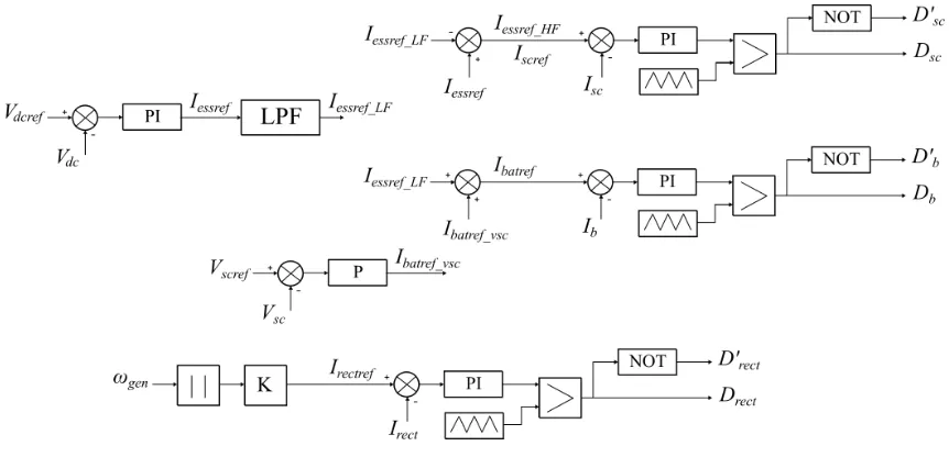
The current reference for battery will be obtained from supercapacitor terminal voltage as well as the average power requirement. Average power requirement can be calculated by using a low pass filter. Low pass filter transfer function can be given as follows,
HLP F(s) = 1 1 +s/ωc
(5.7)
Figure 5.8: Ib control bode plot
ωc = 2πfc (5.8)
= 2π0.01 (5.9)
HLP F(s) = 1 1 +s/ωc
(5.10)
Hence the battery current reference based on average power requirement can be written as,
Iessref LF(s) =HLP F(s)∗iessref(s) (5.11)
Voltage across the supercapacitor Csc can be written as
Vsc(s) =
Isc(s)
Cscs
, (5.12)
Vsc(s) = 1
Cscs
transfer function can be given as follows.
Gibatref vsc(s) =
Vsc(s)
Ibatref2(s) = 1
Cscs
(5.14)
Proportional controller is designed and Kp value is appropriately chosen to achieve 0.01Hz bandwidth for controlling voltage vsc.
Hibatref vsc(s) = 5.188 (5.15)
The plant transfer function, controller and closed loop gain bode plot forVsc control is shown in the Fig. 5.9.
Figure 5.9: vsc control bode plot
We can add the reference currents for battery obtained from both Vsc controller and low pass filter to give the total battery reference current.
5.4.4 System model simulation of hybrid supercapacitor and battery control To provide average current by using battery, a simple low pass filter is used. Reference current generated for supercapacitor by voltage controller is passed through this low pass filter to give average current. Fig. 5.10 is modeled in Simulink for simulation purpose. Controller block diagram for hybrid control is as shown in Fig. 5.12
Figure 5.10: System circuit with hybrid battery and supercapacitor
(a) Load current (b) Rectified Current
(c) Supercapacitor Current (d) Battery Current
(e) Rectifier Voltage (f) Supercapacitor Voltage
Figure 5.12: Hybrid battery and supercapacitor controller
5.4.5 System model hardware implementation using hybrid supercapacitor and battery control
Figure 5.13: Hardware setup for wave energy generation with hybrid energy storage
Figure 5.14: System with hybrid energy storage test in hardware Ch1: Supercapacitor current
5.5
Conclusion
This thesis discussed the integration of hybrid energy storage in oscillatory wave energy genera-tion system to provide smooth power in stand-alone applicagenera-tion. Low cost is achieved by use of diode rectifier as compared to active converter. Hybrid energy storage control is achieved using supercapacitor and DC power supply as battery. Simulation and hardware results are obtained to demonstrate the output power smoothing for resistive load. Hardware results are comparable with the simulation results and it can be seen that hybrid energy storage control is successully achieved. It can be seen that the supercapacitor current intially in hardware result is slightly higher than the one obtained in simulation. This is because in simulation battery current starts gradually increasing as soon as the simulation is started which reduces power requirement from the supercapacitor. But in practical case, battery side boost converter is operated after some delay.
REFERENCES
[1] B. Czech and P. Bauer, ”Wave Energy Converter Concepts : Design Challenges and
Clas-sification” in IEEE Industrial Electronics Magazine, vol. 6, no. 2, pp. 4-16, June 2012.
[2] K. Edwards and M. Mekhiche, ”Ocean power technologies powerbuoy: System-level design,
development and validation methodology” in Proc. Marine Energy Tech. Symp.(METS)
Seattle, WA, USA, 2014.
[3] S. Hazra, S. Bhattacharya, K. K. Uppalapati, and J. Bird, ”Ocean energy power take-off
using oscillating paddle” Proc. IEEE Energy Convers. Congr. and Expo. (ECCE), Raleigh,
NC, USA, 2012, pp. 407413.
[4] L. Cameron, R. Doherty, A. Henry, K. Doherty, J. Vant Hoff, D. Kaye, D. Naylor, S.
Bour-dier, and T. Whittaker, ”Design of the next generation of the oyster wave energy converter”
in Proc. IEEE Int. Conf. on Ocean Energy (ICOE), vol. 6, Bilbao, Spain, 2010.
[5] S. Hazra and S. Bhattacharya, ”Electrical machines for power generation in oscillating
wave energy conversion system A comparative study” in 2015 IEEE International Electric
Machines and Drives Conference, Coeur d’Alene, ID, 2015, pp. 1538-1544.
[6] S. Hazra and S. Bhattacharya, ”Short time power smoothing of a low power wave energy
system” IECON 2012 − 38th Annual Conference on IEEE Industrial Electronics Society,
Montreal, QC, 2012, pp. 5846-5851.
[7] C. Siqi et al. ”Optimal coordinated operation for microgrid with hybrid energy storage
and diesel generator” in Power System Technology (POWERCON), 2014 International
Conference on, Chengdu, 2014, pp. 3207-3212.
[8] H. Lee, B. Y. Shin, S. Han, S. Jung, B. Park and G. Jang, ”Compensation for the Power
Fluctuation of the Large Scale Wind Farm Using Hybrid Energy Storage Applications” in
IEEE Transactions on Applied Superconductivity, vol. 22, no. 3, pp. 5701904-5701904, June
[9] J. Deng, J. Shi, Y. Liu and Y. Tang, ”Application of a hybrid energy storage system in the
fast charging station of electric vehicles” in IET Generation, Transmission & Distribution,
vol. 10, no. 4, pp. 1092-1097, 3 10 2016.
[10] Robert W. Erickson, Dragan Maksimovic, ”Fundamentals of Power Electronics” 2nd
edition, 2004, Kluwer Academic Publishers
[11] Dandan Ma, ”Vector oriented control of voltage source PWM inverter as a dynamic VAR
compensator for wind energy conversion system connected to utility grid” in Doctor of
Philosophy Thesis, Newcastle University, United Kingdom, May, 2012.
[12] M. M. N. Amin and O. A. Mohammed, ”Self-excited Induction Generator A Study Based
on Nonlinear Dynamic Methods” in Applied Power Electronics Conference and Exposition
(APEC), 2010 Twenty-Fifth Annual IEEE, Palm Springs, CA, 2010, pp. 1640-1650.
[13] J. Arrillaga and D. B. Watson, ”Static power conversion from self-excited induction
gener-ators” in Proceedings of the Institution of Electrical Engineers, vol. 125, no. 8, pp. 743-746,
August 1978.
[14] E. Bim, J. Szajner and Y. Burian, ”Voltage compensation of an induction generator with
long-shunt connection” in IEEE Transactions on Energy Conversion, vol. 4, no. 3, pp.
526-530, Sep 1989.
[15] S. Hazra, A. S. Shrivastav, A. Gujarati and S. Bhattacharya ”Dynamic emulation of
oscil-lating wave energy converter” in 2014 IEEE Energy Conversion Congress and Exposition
(ECCE), Pittsburgh, PA, 2014, pp. 1860-1865.
[16] Samir Hazra, Prathamesh Kamat, Ashish Shrivastav, Subhashish Bhattacharya,
”Em-ulation of oscillating wave energy converter for laboratory test bed” in Marine Energy
Technology Symposium, April 27-29, 2015, Washington, DC.
[18] V. Musolino, E. Tironi and P. di Milano, ”A comparison of supercapacitor and high-power
lithium batteries” in Electrical Systems for Aircraft, Railway and Ship Propulsion, Bologna,
2010, pp. 1-6.
[19] S. Sikkabut et al., ”Comparative study of control approaches of Li-Ion
bat-tery/supercapacitor storage devices for fuel cell power plant,” in 2015 International
Con-ference on Clean Electrical Power (ICCEP), Taormina, 2015, pp. 647-652.
[20] L. Jiang and B. J. Arnet, ”Charging Supercapacitors from Low Voltage with an Induction
Machine” in 2007 IEEE Vehicle Power and Propulsion Conference, Arlington, TX, 2007,
pp. 537-543.
[21]
http://www.intersil.com/content/dam/Intersil/whitepapers/switching-controller/supercapacitor-charging.pdf
[22] A. Lahyani, P. Venet, A. Guermazi and A. Troudi, ”Battery/Supercapacitors Combination
in Uninterruptible Power Supply (UPS)” in IEEE Transactions on Power Electronics, vol.