ABSTRACT
MUNDKUR, SAMEER SHAILESH. Design and implementation of a Digital Controller for High Power Converters. (Under the direction of Professor Alex Q. Huang.)
Multi-level converter topologies are widely used in utility power electronics as it offers improved reliability, multiple layers of protection, flexibility of expansion and isolation.
This thesis proposes to design and implement a distributed control topology for high power electronics which consists of centralized controller which would process various power electronic related signals like voltage, current, switching device temperatures as well as several localized controllers which communicate with the central controller and generate gate drive signals for each high power switching device/ bridge converter. So there is essentially a two layer hierarchy – the complex digital signal processing and modulation algorithms are done at the central controller level and the switching modulation signals are then sent to several localized controllers which then process this data and control the power electronics. The central controller provides the supervisory control while the actual device level control is delegated to several local controllers. This topology provides flexibility as well as a robust communication scheme between controllers. This thesis also looks at a shared control algorithm computation approach by moving some of the computation from the DSP to the FPGA for faster processing and generation of gate drive control.
Design and implementation of a Digital Controller for High Power Converters
by
Sameer Shailesh Mundkur
A thesis submitted to the Graduate Faculty of North Carolina State University
in partial fulfillment of the requirements for the Degree of
Master of Science
Electrical Engineering
Raleigh, North Carolina 2008
APPROVED BY:
Dr. Subhashish Bhattacharya Dr. Mesut Baran
Dr. Alex Q. Huang Chair of Advisory Committee
BIOGRAPHY
Sameer Shailesh Mundkur was born in Pune, India. He received the Bachelor of Engineering degree in Electronics Engineering from University of Pune in 2005. He worked for about a year and a half as an Electronic Design Engineer at Honeywell Automation India Limited, Pune, India.
ACKNOWLEDGEMENTS
I wish to express sincere appreciation to my advisor Dr. Alex Q. Huang for his illuminating guidance and timely advice throughout this project. It was a truly an enlightening experience to work with one of the leaders in the world of Power Electronics research. Throughout my two year stay at the SPEC lab in NCSU, I have had the fortune of working with some of the most brilliant minds.
Dr. Subhashish Bhattacharya, has always been a great source of inspiration. His suggestions and feedback during our weekly SPEC team meetings has been a driving force getting this project to this level of success. I would also like to thank Dr. Mesut Baran for sharing his knowledge on power systems aspects of the controller.
I would like to thank all my student colleagues with whom I have spent countless hours in the Lab - Anand, Rahul, Shoubhik, Peter, Zhigang, Wenchao, Xiaohu, Jun, Tiefu, Liyu helped create the fun and stimulating environment that it was. We will be best of friends. I’ve had some great friends Sudhakar, Ashish, Wilfred, Prakhyath over the course of 2 years studying, working on projects and assignments or just having fun. I found a bunch of excellent roommates in Saurabh, Nitin, Kanishka, Rikin and Mohan. Life at NC State was complete thanks to all these guys.
TABLE OF CONTENTS
LIST OF TABLES... vi
LIST OF FIGURES ... vii
Chapter 1. Introduction... 1
1.1. Overview... 1
1.2. Previous Work ... 2
1.3. Organization... 2
Chapter 2. Controller Architecture ... 4
2.1. Existing Controller Architecture... 4
2.2. Proposed Controller Architecture ... 7
2.3. Multi –Layered Protection scheme ... 11
Chapter 3. Local Controller... 13
3.1. External Controller Interface signals ... 15
3.2. Gate Driver logic and switch state decoding ... 19
3.3. Sensor signal Decoding and collection... 25
3.3.1. PWM decoding Logic... 28
3.3.2. Sensor signal decoding Logic ... 29
3.3.3. Sensor signal registers... 31
3.3.4. Experimental Results – Sensor signal PWM Outputs Vs Input... 32
3.4. Communication between Local and Central Controller ... 34
3.4.1. Serial Transmitter Module ... 37
3.5. Local Protection... 42
3.5.1. Over Voltage Protection Module... 43
3.5.1.1. Over voltage control strategy... 43
3.5.1.2. Over voltage protection logic... 44
3.5.2. Over Current Protection Module ... 48
3.5.2.1. Over Current control strategy ... 48
3.5.2.2. Over Current Protection Logic... 50
3.5.3. Over Temperature Protection Module ... 53
3.5.3.1. Over Temperature control strategy ... 53
3.5.3.2. Over temperature protection logic ... 55
3.5.4. Feedback Check Protection Module ... 58
3.5.4.1. Feedback check control strategy... 59
3.5.4.2. Feedback check protection logic... 60
3.5.5. On Board Fault indicators... 63
Chapter 4. Central controller ... 65
4.5. PCI FPGA Receiver Module ... 84
4.6. PCI FPGA Transmitter Module... 86
4.7. ADC Interface Module ... 88
4.8. PWM Calculation and Gating signal generation Module... 95
4.8.3. Moving Angle Calculation block... 101
4.8.4. 5 to 20 angle Calculation block ... 102
4.8.5. SPWM – Calculation block ... 104
Chapter 5. Results and Conclusion... 107
5.1. Hardware Simulation ... 107
5.2. Conclusion and recommendations for future work... 110
LIST OF TABLES
Table 3-1 – Interface signals and functions ... 17
Table 3-2 – List of Local Controller Modules and functions ... 18
Table 3-3 – Switch state Decoding table ... 19
Table 3-4 – Sensor Signal register format ... 31
Table 3-5 – Sensor Signal Register Names and functions... 31
Table 3-6 – Data Frame protocol ... 35
Table 3-7 – Sensor selector value and description... 36
Table 3-8 - Serial transmitter frame transmission sequence... 39
Table 3-9 – Voltage data frame format... 39
Table 3-10 – Current Data frame format ... 40
Table 3-11 – Temperature Data frame format ... 40
Table 3-12 – Error Flags Data frame format ... 40
Table 3-13 – Fault indicator and type of fault ... 63
Table 3-14 – Feedback Fault indicator and type... 64
Table 4-1 – Central Controller interface signals... 68
Table 4-2 – List of Central Controller Modules and Functions... 69
Table 4-3 – Bus Direction Control Logic ... 77
Table 4-4 – DSP Memory Mapped address and FPGA data on Data_Bus ... 80
Table 4-5 - DSP Memory Mapped address and FPGA data input on Data_Bus... 83
Table 4-6 – PCI FPGA serial frame format ... 84
Table 4-7 – PCI Transmitted data Frame Decoder table ... 85
Table 4-8 – Switch PWM data frame format... 87
Table 4-9 – HMI data frame format... 87
Table 4-10 – Control Register 0 (CR0) format... 91
Table 4-11 – Control Register 1 (CR1) format... 91
LIST OF FIGURES
Figure 2-1 – Existing Control Architecture Highlighting the communication bottleneck ... 4
Figure 2-2 – Existing Controller Architecture based... 5
Figure 2-3 – Proposed Controller Architecture ... 8
Figure 2-4 - Detailed Block diagram of proposed architecture ... 10
Figure 2-5 – Multi layered protection scheme... 11
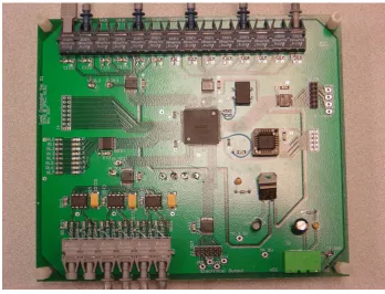
Figure 3-1 - Local Controller Board Prototype... 14
Figure 3-2 – Local Controller Internal Block Diagram ... 15
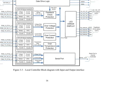
Figure 3-3 – Local Controller Block diagram with Input and Output interface ... 16
Figure 3-4 – ETO based H Bridge converter ... 19
Figure 3-5 – Gate Driver Logic Module ... 20
Figure 3-6 – Gate Driver Module Finite State Machine – State Transition Diagram... 23
Figure 3-7 – Gate driver module simulation waveforms ... 24
Figure 3-8 – Multiplexed sensor signal decoding... 26
Figure 3-9 – Multiplexed Sensor signal decoding RTL simulation waveforms... 27
Figure 3-10 – PWM generation logic in the ETO board ... 28
Figure 3-11 – Sensor signal decoding FSM state transition diagram ... 29
Figure 3-12 – Sensor temperature / ETO temperature decoder module ... 30
Figure 3-13 – Voltage / current sensor decoder module... 30
Figure 3-14 – Voltage Sensor Curve ... 32
Figure 3-15 – Temperature sensor Curve ... 33
Figure 3-16 – Asynchronous Serial communication format... 34
Figure 3-17 – Serial transmitter module ... 37
Figure 3-18 – Serial Transmitter finite state machine (FSM) state transition diagram ... 38
Figure 3-19 – Serial Transmitter module RTL simulation waveforms... 41
Figure 3-20 – Over – Voltage protection Module ... 43
Figure 3-21 – Over Voltage FSM state transition diagram... 44
Figure 3-22 – Over – Voltage Protection scheme... 46
Figure 3-23 – Over Voltage Protection simulation waveforms ... 47
Figure 3-24 – Over Current Protection Module... 48
Figure 3-25 – Over current FSM state transition diagram... 50
Figure 3-26 – Over Current Protection scheme ... 51
Figure 3-27 - Over Current Protection scheme simulation waveforms ... 52
Figure 3-28 Over – temperature module... 53
Figure 3-29 – Over – Temperature FSM state transition diagram... 55
Figure 3-30 – Over temperature Protection scheme ... 56
Figure 3-31 - Over temperature Protection simulation waveforms ... 57
Figure 3-32 – Feedback check protection module... 58
Figure 3-33 – Feedback check protection FSM state transition diagram ... 60
Figure 3-34 – Feedback check protection sequence ... 61
Figure 4-1 – Central Controller Internal Block Diagram... 66
Figure 4-2 – Serial Receiver Module at the Central Controller... 70
Figure 4-3 – Clock Domain Crossing – Double Flop Synchronizer... 71
Figure 4-4 – Serial frame showing START and STOP end delimiters... 72
Figure 4-5 – Receiver clock generation and synchronization... 74
Figure 4-6 – Asynchronous Serial receiver Detailed internal block diagram... 75
Figure 4-7 – Serial Receiver Module simulation waveforms ... 76
Figure 4-8 – DSP to FPGA bus interface module ... 77
Figure 4-9 – DSP Transmitter module... 79
Figure 4-10 – DSP receiver module... 82
Figure 4-11 – PCI FPGA Receiver Module... 84
Figure 4-12 – PCI FPGA transmitter Module... 86
Figure 4-13 – ADC interface module ... 88
Figure 4-14 – THS1206 Control register initialization sequence ... 90
Figure 4-15 – ADC Power Up initialization sequence simulation waveforms... 92
Figure 4-16 – ADC THS1206 internal block Diagram... 93
Figure 4-17 – Single Conversion Mode ADC timing diagram... 94
Figure 4-18 – ADC data read timing diagram ... 95
Figure 4-19 – Block diagram of the SPWM calculation and gate generation module ... 96
Figure 4-20 - DSP algorithm and Calculation bottleneck resolution using FPGA... 97
Figure 4-21 – PLL value interpolation and calculation waveforms ... 98
Figure 4-22 - DC Offset seen in the Current waveforms due to computation delay in DSP.. 99
Figure 4-23 - DC offset eliminated after computation moved to FPGA ... 99
Figure 4-24 – Optimum Modulation waveforms... 100
Figure 4-25 – Moving angle calculation module... 101
Figure 4-26 – 5 to 20 angle calculation block... 102
Figure 4-27 – PWM calculation block... 104
Figure 4-28 – Switching angles and Moving angle comparison... 104
Figure 4-29 – SPWM calculation module simulation waveforms... 106
Figure 5-1 - System Diagram of STATCOM Prototype used for hardware in loop test ... 108
Chapter 1.
Introduction
1.1.
Overview
Multi-level converter topologies are widely used in utility power electronics as it offers improved reliability, multiple layers of protection, flexibility of expansion and isolation.
This thesis proposes to design and implement a multilevel control topology for high power electronics which consists of centralized controller which would process various power electronic related signals like voltage, current, switching device temperatures as well as several localized controllers which communicate with the central controller and generate actual gate drive signals for each high power switching device/ bridge converter. So there is essentially a two layer hierarchy – the complex digital signal processing and modulation algorithms are done at the central controller level and the switching modulation signals are then sent to several localized controllers which then process this data and control the power electronics. The central controller provides the supervisory control while the actual device level control is delegated to several local controllers. This topology provides flexibility as well as a robust communication scheme between controllers.
The design and implementation of the controller addresses some of the major challenges faced by typical High power converter applications which demand fail-safe fault protection, accurate control and expansion flexibility for increase in power rating.
response and corrective action in case of voltage and current fault conditions and bring the switching device / converter to a safe state of operation during a fault condition.
The central controller, processes the data from the multiple local controllers and provides overall system level control
This implementation of an intelligent localized controller would result in better performance and fault-response time through the exploitation of parallelism inherent in a programmable hardware (FPGA) based controller approach. The design is captured using synthesizable Verilog HDL and synthesized on a FPGA.
1.2.
Previous Work
The digital controller for Cascaded Multi-level Converter (CMC) based static synchronous compensators (STATCOM) systems proposed by Zhaoning Yang [2] and Wenchao Song [8] is used as a reference point for developing the controller in this lab. The basic controller hardware boards used in thesis have been the same central controller DSP + FPGA board – the Signalware AED-106 board with the TMS320C6713 DSP and Xilinx Virtex XCV300 on it. The Local controller board used is a modified version of the earlier local controller using the Altera Flex EPF10KA30 FPGA [3], [4] with more logic and I/O capability.
Chapter 2.
Controller Architecture
2.1.
Existing Controller Architecture
The digital controller for Cascaded Multi-level Converter (CMC) based static synchronous compensators (STATCOM) systems proposed by Zhaoning Yang [2] in 2006 has been used as a starting point in this thesis. This thesis aims at identifying the shortcomings of the existing architecture in terms of both control and additional features required by high power controllers.
The existing architecture of this system consists of a distributed controller approach where there is a localized controller for each high power bridge and a central controller for overall system level control.
system unnecessarily large, complex and introduces additional inter-board communication overhead.
Figure 2-2 – Existing Controller Architecture based
This existing system of communication was designed primarily for data acquisition and display at the central controller end. With more features being added to the local controllers and the need for a layered protection scheme, this communication bottleneck in the existing architecture poses a serious problem.
A detailed analysis of the communication bottleneck is as under –
• Serial communication speed from Local to Signal collection board – 250kbps = 4us bit time
• Size of Data frame from Local Controller to signal collection board- 18 bits
• Total Number of data frames to be sent from local to signal collection board – 4 Voltage, 4 Current, 4 temperature, 4 error flag = 16 frames
• Total time to transmit 16 frames to signal collection FPGA = 16 x 18 x 4us = 1.15ms The Sensor signal collection board basically requires at least 1.15 ms for collecting the data from the local controllers. It then consolidates all this data from the local controllers and then sends this data back serially to the Central controller / DSP in a specified framing format
• Serial communication speed from Signal collection board to central controller – 250kbps = 4us bit time
• Size of Data frame from signal collection board to central controller - 18 bits
• Total Number of data frames to be sent from Signal collection board to central controller – 4 Voltage, 4 Current, 4 temperature, 4 error flag = 16 frames
• Total number of Local controllers = 6
• Total time to transmit all this data from signal collection board to Central controller = 6 x 16 x 18 x 4us = 6.9 ms
Total communication delay between the Local controllers and Central controller is more than 8 ms.
central controller FPGA, however this can be overcome by optimum I/O port usage at the central controller end. Furthermore from the communication delay that was calculated above, it is clear that the system delay of >8ms for signal acquisition and transfer makes this data unusable real time control and protection by the time it is transmitted and available at the central controller.
2.2.
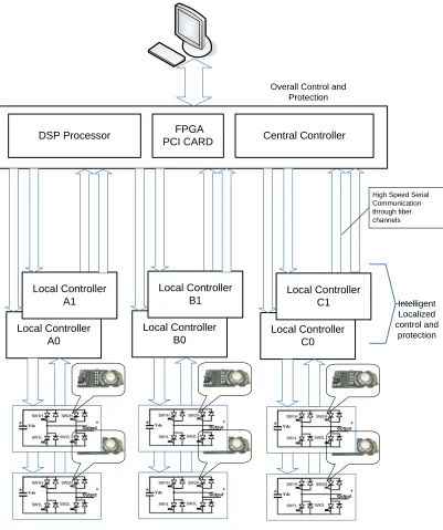
Proposed Controller Architecture
Local Controller A0
Local Controller A1
Local Controller B0
Local Controller B1
Local Controller C0
Local Controller C1 Central Controller
DSP Processor FPGA
PCI CARD
High Speed Serial Communication through fiber channels
Intelligent Localized control and
protection Overall Control and
Protection
Figure 2-3 – Proposed Controller Architecture
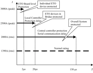
2.3.
Multi –Layered Protection scheme
I
1390A (rms) 2000A (rms) 2500A (peak) 3000A (peak)
2µs 20µs 150 µs T
Normal rating Central controller protection Serial communication delay Local Controller
Protection delay ETO Board level Protection
Individual ETO device protected
ETO devices in Bridge protected
Overall System protected
Figure 2-5 – Multi layered protection scheme
As shown in Figure 2-5 a robust modular controller scheme requires multiple levels of protection at each level in the hierarchy.
ETO Board level
The ETO board also contains inbuilt protection mechanism which triggers at a much higher threshold level as compared to the threshold programmed for the local and central controller levels.
Local controller Level
controller will identify which device is in protection state and send all this data over to the next level in the hierarchy for system level corrective action.
Central controller Level
Chapter 3.
Local Controller
The local controller [5] is FPGA based controller, which can be used to control a modular converter. This forms the basic building block in the modular controller topology with one local controller for each bridge converter in the system. The main requirements of a localized controller for each bridge in the system are -
• A Localized controller provides smart control of each switching device in the bridge.
• Monitoring device parameters - current, voltage, temperature as well as the sensor temperature for compensation.
• Locally processes this data to implement smart protection schemes
• Sends diagnostic data to central controller for system level corrective action.
The local controller must also provide the following protection features
• Over –Voltage Protection – when any of the devices in the bridge exceed the voltage threshold
• Over – Temperature protection with Fan control - when any of the devices in the bridge exceed the temperature threshold.
• Over – Current protection with Auto Switch Re-closure – An automatic protect and reclose scheme is required when the devices exceed the over-current threshold
• Smart loss of sensor signal feedback protection Features
• Localized control provides real-time response and corrective action during faults
• Inherent parallelism in FPGA based controller - results in better performance and faster – response time
• Guaranteed dead-band between switching states – prevent shoot-through
• Zero- Vector rotation every 25ms to ensure uniform losses in zero state
• Intelligent Device Over – Temperature monitoring and protection with Fan control
• Intelligent Device Over – Voltage protection with hysteretic control action
• Smart loss of sensor signal feedback protection
• Implemented in synthesizable Verilog
• Fully optical interface
• Fully compatible with any optically triggered switch
• Serial communication with other controllers
• Suitable for different converter topologies
3.1.
External Controller Interface signals
Local controller [6] has 12 sensor signal inputs, 3 sensor inputs for each of the 4 ETO devices in a bridge and 2 modulation signal inputs from the DSP. The Local controller generates 6 outputs, 4 outputs one for each ETO device, one Serial output to the Central controller and then a Fan control output in case of over temperature. All the inputs and outputs are optical interfaces providing the high voltage isolation and noise immunity required in High voltage industrial applications.
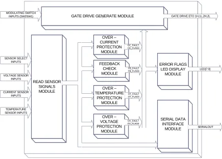
MODULATING SWITCH INPUTS (SW2SW1) CURRENT SENSOR INPUTS VOLTAGE SENSOR INPUTS SENSOR SELECT INPUTS TEMPERATURE SENSOR INPUTS READ SENSOR SIGNALS MODULE
Figure 3-2 – Local Controller Internal Block Diagram
GATE DRIVE GENERATE MODULE
SERIAL DATA INTERFACE MODULE OVER – CURRENT PROTECTION MODULE OVER – VOLTAGE PROTECTION MODULE OVER – TEMPERATURE PROTECTION MODULE FEEDBACK CHECK MODULE OC_FAULT, OC_FLAGS FB_FAULT FB_FLAGS OT_FAULT OT_FLAGS OV_FAULT OV_FLAGS
GATE DRIVE ETO 1H,1L,2H,2L
ERROR FLAGS LED DISPLAY
MODULE
LED[7:0]
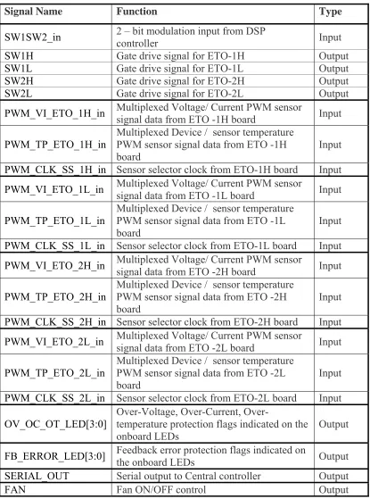
Table 3-1 – Interface signals and functions
Signal Name Function Type
SW1SW2_in 2 – bit modulation input from DSP controller Input SW1H Gate drive signal for ETO-1H Output SW1L Gate drive signal for ETO-1L Output SW2H Gate drive signal for ETO-2H Output SW2L Gate drive signal for ETO-2L Output
PWM_VI_ETO_1H_in Multiplexed Voltage/ Current PWM sensor signal data from ETO -1H board Input
PWM_TP_ETO_1H_in
Multiplexed Device / sensor temperature PWM sensor signal data from ETO -1H board
Input
PWM_CLK_SS_1H_in Sensor selector clock from ETO-1H board Input
PWM_VI_ETO_1L_in Multiplexed Voltage/ Current PWM sensor
signal data from ETO -1L board Input
PWM_TP_ETO_1L_in
Multiplexed Device / sensor temperature PWM sensor signal data from ETO -1L board
Input
PWM_CLK_SS_1L_in Sensor selector clock from ETO-1L board Input
PWM_VI_ETO_2H_in Multiplexed Voltage/ Current PWM sensor
signal data from ETO -2H board Input
PWM_TP_ETO_2H_in
Multiplexed Device / sensor temperature PWM sensor signal data from ETO -2H board
Input
PWM_CLK_SS_2H_in Sensor selector clock from ETO-2H board Input
PWM_VI_ETO_2L_in Multiplexed Voltage/ Current PWM sensor
signal data from ETO -2L board Input
PWM_TP_ETO_2L_in
Multiplexed Device / sensor temperature PWM sensor signal data from ETO -2L board
Input
PWM_CLK_SS_2L_in Sensor selector clock from ETO-2L board Input
OV_OC_OT_LED[3:0]
Voltage, Current,
Over-temperature protection flags indicated on the
onboard LEDs Output
FB_ERROR_LED[3:0] Feedback error protection flags indicated on the onboard LEDs Output
SERIAL_OUT Serial output to Central controller Output
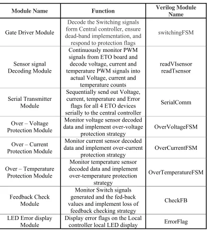
The various functions within the local controller have been broken into distinct logical modules. This makes the overall structure of the controller code easier to maintain and modify for future changes and feature upgrades.
Table 3-2 – List of Local Controller Modules and functions
Module Name Function Verilog Module Name
Gate Driver Module
Decode the Switching signals form Central controller, ensure dead-band implementation, and
respond to protection flags
switchingFSM
Sensor signal Decoding Module
Continuously monitor PWM signals from ETO board and decode voltage, current and temperature PWM signals into
actual Voltage, current and temperature counts
readVIsensor readTsensor
Serial Transmitter Module
Sequentially send out Voltage, current, temperature and Error
flags for all 4 ETO devices serially to the central controller
SerialComm
Over – Voltage Protection Module
Monitor voltage sensor decoded data and implement over-voltage
protection strategy
OverVoltageFSM
Over – Current Protection Module
Monitor current sensor decoded data and implement over-current
protection strategy
OverCurrentFSM
Over – Temperature Protection Module
Monitor temperature sensor decoded data and implement
over-temperature protection strategy
OverTemperatureFSM
Feedback Check Module
Monitor Switch signals generated and the fed-back values and implement loss of
feedback checking strategy
CheckFB
3.2.
Gate Driver logic and switch state decoding
The Central controller generates and sends a two bit encoded switch state signal. The two switch states input can be used to generate two pairs of complementary switching signals to drive the 4 ETO devices in the bridge converter directly.
{SW2, SW1} = 00 - All 4 devices SW1H, SW1L, SW2H, SW2L are OFF
{SW2, SW1} = 01 - 2 devices SW1H = OFF, SW1L = ON, SW2H = ON, SW2L = OFF {SW2, SW1} = 10 - 2 devices SW1H = ON, SW1L = OFF, SW2H = OFF, SW2L = ON {SW2, SW1} = 11 - 2 devices SW1H = ON, SW1L = OFF, SW2H = ON, SW2L = OFF Also an all-off state is generated to deal with the diode charge mode or protection mode.
Table 3-3 – Switch state Decoding table
{SW2, SW2} 00 01 10 11
SW1H 0 0 1 1
SW1L 0 1 0 0 SW2H 0 1 0 1
SW2L 0 0 1 0 Output X -Vdc +Vdc 0
For a typical H-bridge 3-level converter, the relationship between output and switch state input is shown below.
Vdc
+
SW1H SW1L SW2H SW2LOutput
+
Vdc
+
SW1H SW1L SW2H SW2LOutput
+
The main functions of the switch decoder module are
• Decode the switch state signals from the central controller, protect the devices in the bridge in case of over-current, over-voltage or over-temperature,
• Ensure a 25us dead band between switching states guarantee that there is no shoot through in any of the arms of the H – bridge.
• Another feature that has been implemented in order to keep all switches and diode having the same loss in the H - bridge, the two possible zero voltage vectors rotate within the H - Bridge, every 25 ms (needs to be smaller than heat-pipe thermal constant).
Figure 3-5 – Gate Driver Logic Module
The ETO driver module has inputs from the protection modules that indicate fault condition. In case of a fault condition, all the 4 devices in the bridge SW1H, SW1L, SW2H and SW2L are switched. For NORMAL operation when no fault exists, the switches follow the decoded SW1SW2 signal from the central controller implementing the required dead-band and zero vector rotation feature.
At the core of the driver module is a Finite state machine [15] with 10 states
NORMAL10 - This is the state when the SW2SW1 = 10. During this state the switches SW1H = 1, SW1L = 0, SW2H = 0, SW2L = 1.
NORMAL11_0 – This is one of the possible zero vector states. This is the state when the SW2SW1 = 11. During this state the switches SW1H = 1, SW1L = 0, SW2H = 1, SW2L = 0.
NORMAL11_1 - This is the other possible zero vector state. This is the state when the SW2SW1 = 11. During this state the switches SW1H = 0, SW1L = 1, SW2H = 0, SW2L = 1.
DELAY01 – This is the intermediate dead-band state that is entered before a transition on SW2SW1 to NORMAL01. In this state the other two switches in the bridge that should be turned off before turning ON the other pair are switched off - SW1H = 0 and SW2L=0.
It remains in this state for 25us and then transitions to the NORMAL01 state, thereby ensuring that the previous devices that are ON are turned OFF before the next two are turned ON.
DELAY10 – This is the intermediate dead-band state that is entered before a transition on SW2SW1 to NORMAL10. In this state the other two switches in the bridge that should be turned off before turning ON the other pair are switched off - SW1L = 0 and SW2H=0.
It remains in this state for 25us and then transitions to the NORMAL10 state, thereby ensuring that the previous devices that are ON are turned OFF before the next two are turned ON
DELAY11_0 – This is the intermediate dead-band state that is entered before a transition on SW2SW1 to NORMAL11_0. In this state the other two switches in the bridge that should be turned off before turning ON the other pair are switched off - SW1H = 0 and SW2H=0. It remains in this state for 25us and then transitions to the NORMAL11_0 state, thereby ensuring that the previous devices that are ON are turned OFF before the next two are turned ON.
It remains in this state for 25us and then transitions to the NORMAL11_1 state, thereby ensuring that the previous devices that are ON are turned OFF before the next two are turned ON
FAULT – This is the state that is entered when any of the protection error flags are set. During this state all the switches SW1H = 0, SW1L = 0, SW2H = 0, SW2L = 0.
Thus between any transition of SW2SW1 to a new value the state machine enters the corresponding DELAY state during which a 25us counter is started. Once the counter reaches the desired 25us delay the counter is reset and the state machine enters the next switching state according to the value on SW2SW1.
For the zero vector rotation when SW2SW1 = 11, a 25 ms counter is used that overflows every 25ms. So when the switch state inputs SW2SW1= 11, and remains in this state for more than 25ms, the zero vector rotation sequence is activated and the state machine will change form NORMAL11_0 to NORMAL11_1 after transitioning through the 25ms dead-band delay time.
FAULT NORMAL00 NORMAL11 0 NORMAL11 1 NORMAL10 NORMAL01 DELAY11 1 DELAY11 0 DELAY10 DELAY01
reset
3.3.
Sensor signal Decoding and collection
ETO devices send out sensor signals – Voltage, Current, Sensor Temperature and device temperature in a Time Multiplexed format that is synchronized to a sensor selector signal also generated and sent along with the sensor signals. The ETO devices send out the sensor signal in the form of a time multiplexed Pulse width modulated (PWM) signal. When the synchronizing switch selector (PWM_CLK_SS) is at logic high, the PWM signal at PWM_VI_ETO represents the Device current and when the synchronizing switch selector is at logic low, the PWM signal at PWM_VI_ETO represents the voltage across the ETO Device.
Similarly, the other multiplexed temperature signal input line PWM_TP_ETO represents the sensor temperature when the synchronizing switch selector is at logic high and represents the ETO device cathode temperature when the synchronizing switch selector (PWM_CLK_SS) is at logic low.
Each Local controller is capable of processing the sensor data from 4 ETO devices and decoding them into an actual voltage, current and temperature value that is then used internally to provide rapid response and protection in case voltage, current, over-temperature condition is detected.
PWM_VI_ETO
PWM_TP_ETO
Pulse Width proportional to Sensor Temperature
Pulse Width proportional to ETO
Temperature
ultiplexed Voltage / urrent PWM signal)
ultiplexed Device / sensor Temperature
PWM signal)
PWM_CLK_SS
Pulse Width proportional to Device Current
Pulse Width proportional to Device Voltage
MULTIPLEXED SENSOR SIGNALS FROM ETO BOARD
(Sensor selector signal)
(M C
(M
3.3.1.
PWM decoding Logic
The PWM generation for the sensor signals is done on the ETO device board using the IRF2175 IC with a datasheet specification of PWM carrier frequency output ranging from 100Khz (min) to 130Khz (typ.) and 180KHz(max).
Anode
Over-S
PWM
Figure 3-10 – PWM generation logic in the ETO board
Now the Local controller internally uses a 40MHz oscillator for a clock so the maximum sensor signal resolution that can be obtained is counting the Pulse width Modulated (PWM) pulse ON and OFF time pulse widths in increments of 25 ns
Local Controller Clock frequency = 40 MHz. Period = 1/40 MHz = 25ns.
Generator Gate Switch GT Cathode Comparator &Latch Protection Optical Output Vt Emitter Switch & Its Temp. Sensor
R1
Ve Vi
Temperature Compensated
frequency of 100 KHz and 100% duty cycle, the maximum number of bits required to store the sensor count would be given by the following calculation –
Slowest PWM carrier frequency = 100 KHz Local Controller clock frequency = 40 MHz Count for 100% duty cycle = 40 Mhz/100Khz = 400
Number of bits required to represent this = log2(400) = 9 bits.
3.3.2.
Sensor signal decoding Logic
The Local controller sensor decoder is implemented using a 3 state Finite state machine [16] (FSM)
WAIT COUNT LATCH
reset
Figure 3-11 – Sensor signal decoding FSM state transition diagram
WAIT - This is the default state that the controller enters on power up and waits in this state until the required conditions are met to start the counting. The require conditions are the sensor switch selector and the PWM sensor signal voltage level.
COUNT – When the condition for measuring the pulse ON time is met the FSM enters the count state. In this state the Pulse width ON time count is incremented every clock cycle thereby the PWM On time width is measured in increments of the clock (25ns).
There are 8 such sensor decoders –
4 corresponding to each of the 4 ETO devices – 1H, 1L, 2H, 2L in the bridge for device/ sensor temperature
Sensor temperature / ETO temperature Decoder Module
Figure 3-12 – Sensor temperature / ETO temperature decoder module
4 corresponding to each of the 4 ETO devices – 1H, 1L, 2H, 2L in the bridge for device Current/Voltage. All the 8 sensor decoders’ work in parallel providing real time sensor decoding action required for rapid protection and control.
Voltage / Current Sensor decoder Module
3.3.3.
Sensor signal registers
Table 3-4 – Sensor Signal register format
8 7 6 5 4 3 2 1 0
9-bit sensor signal count corresponding to PWM ON -Time
Table 3-5 – Sensor Signal Register Names and functions
Register Name Function
PWM_V_ETO1H_count Decoded Voltage sensor Value for ETO – 1H PWM_V_ETO1L_count Decoded Voltage sensor Value for ETO – 1L PWM_V_ETO2H_count Decoded Voltage sensor Value for ETO – 2H PWM_V_ETO2L_count Decoded Voltage sensor Value for ETO – 2L
PWM_I_ETO1H_count Decoded Current sensor Value for ETO – 1H PWM_I_ETO1L_count Decoded Current sensor Value for ETO – 1L PWM_I_ETO2H_count Decoded Current sensor Value for ETO – 2H PWM_I_ETO2L_count Decoded Current sensor Value for ETO – 2L
PWM_T_ISens_ETO1H_count Decoded sensor Temperature Value for ETO – 1H PWM_T_ISens_ETO1L_count Decoded sensor Temperature Value for ETO – 1L PWM_T_ISens_ETO2H_count Decoded sensor Temperature Value for ETO – 2H PWM_T_ISens_ETO2L_count Decoded sensor Temperature Value for ETO – 2L
3.3.4.
Experimental Results – Sensor signal PWM Outputs Vs Input
The PWM sensor output from the ETO board was tested over a voltage range of 0 to 2000 Volts and the variation of voltage sensor output PWM duty cycle from the ETO board was plotted against voltage. Figure 3-14 shows the graphical variation of PWM duty cycle with voltage, the graph shows a nearly linear increase of PWM duty cycle with voltage
Voltage Sensor Curve
y = 0.0001x + 0.5114
0.5 0.55 0.6 0.65 0.7 0.75 0.8
0 500 1000 1500 2000
Voltage
Du
ty
Cy
c
le
Voltage sensor curve Linear (Voltage sensor curve)
Figure 3-14 – Voltage Sensor Curve
Temperature curve
y = 0.0024x + 0.6526
0.74 0.76 0.78 0.8 0.82 0.84 0.86
40 50 60 70 80 90
Temperature
D
u
ty C
ycl
e
ETO# duty Linear (ETO# duty)
3.4.
Communication between Local and Central
Controller
In the proposed controller architecture, asynchronous serial communication protocol has been adopted. In high power electronics applications such as this, with a distributed architecture, long distances are involved between the central controller and the distributed local controllers. Considering this sending digital data in parallel over a long distance, would mean more wiring costs and more failure nodes being introduced into the system.
So in the proposed controller, Serial communication has been adopted – fewer interconnections thereby reducing the failure nodes for the whole system and hence increasing the overall system reliability.
The possible transmission line medium for serial communication can be traditional wires, optical fiber [17] or a wireless link. To get lowest signal attenuation and good signal integrity along with high voltage isolation, optical fiber links are adopted in the modular controller application.
The Universal Asynchronous Receiver Transmitter (UART) is the most widely used serial data communication circuit ever. UARTs allow full duplex communication over a single communication line. Asynchronous serial communication makes use of the frame start and stop bit for the purpose of synchronization. The basic functions of the serial asynchronous transmitter module are buffering of transmitter data, frame generation, parity generation, parallel to serial conversion.
The frame format of used by the serial transmitter module is a low start bit, 4 header data bits, 9 data bits, 1 parity bit, and 2 stop bits. The frame format for data transmitted is given in Figure 3-16
S
It consists of a high idle state of the line. A character is from 1-14 data bits. The start bit is Low and the single stop bit is high.
Serial communication baud rate is 2.5Mbps. Every data frame consists of 18 bits. With 1 start bit, a 4 bit header that indicates what the payload data contains, the header is followed by 9-bits of data representing Voltage, current, temperature or error flags. This is followed by a parity bit and then two stop bits.
The data protocol is shown in Table 3-6
Table 3-6 – Data Frame protocol
0 1 2 3 4 5 6 7 8 9 10 11 12 13 14 15 16
0 Start Bit
4-bit Sensor selector
9-bit
Data – Voltage/ current / Temperature/ Flags
1-bit Parity
The 4-bit sensor selector table is defined as
Table 3-7 – Sensor selector value and description
SENSOR SELECTOR Description
0000 Voltage of device 1H 0001 Current of device 1H
0010 Cathode temperature of device 1H 0011 Error Flags of device 1H
0100 Voltage of device 1L 0101 Current of device 1L
0110 Cathode temperature of device 1L 0111 Error Flags of device 1L
1000 Voltage of device 2H 1001 Current of device 2H
1010 Cathode temperature of device 2H 1011 Error Flags of device 2H
1100 Voltage of device 2L
3.4.1.
Serial Transmitter Module
The serial transmitter module transmits all the sensor related data – Voltage, current, temperature from all the four ETO devices in the bridge along with the Fault flags / status bits from the over-current, over-voltage, over-temperature protection modules and then sequentially sends out the data for each device frame by frame.
The block level schematic of the serial transmitter module is as shown in Figure 3-17.
Figure 3-17 – Serial transmitter module
Loadsensor=1 Loadsensor=0
V_ETO_1H I_ETO_1H T_ETO_1H F_ETO_1H
V_ETO_2H I_ETO_2H T_ETO_2H F_ETO_2H F_ETO_1L T_ETO_1L I_ETO_1L V_ETO_1L
F_ETO_2L T_ETO_2L I_ETO_2L V_ETO_2L
Figure 3-18 – Serial Transmitter finite state machine (FSM) state transition diagram
Thus 16 frames need to be transmitted for the local controller to completely transfer the current state of the 4 ETO devices to the central controller.
The serial transmission baud rate = 2.5Mbps. One bit time = 1 / 2.5M = 400 ns
controller FPGA, this means that sensor and error flags for all the 3 phases A0,A1, B0,B1, C0,C1 are transmitted to the central controller within the same time 115 uS.
This is an example frame sequence transmitted by the local controller -
Table 3-8 - Serial transmitter frame transmission sequence
Voltage ETO-1H Current ETO-1H Temp ETO-1H Error Flags ETO-1H Voltage ETO-1L Current ETO-1L Temp ETO-1L Error Flags ETO-1L Voltage ETO-2H Current ETO-2H Temp ETO-2H Error Flags ETO-2H Voltage ETO-2L Current ETO-2L Temp ETO-2L Error Flags ETO-2L
Example Voltage Data frame sent from Local controller to Sensor signal FPGA
The Voltage frame consists of 4 header bits which are used to identify which ETO device the payload data bits correspond to
Table 3-9 – Voltage data frame format
0 1 2 3 4 5 6 7 8 9 10 11 12 13 14 15 16
0 Start bit
4-bit
Sensor selector
0000 – Voltage 1H 0100 – Voltage 1L 1000 – Voltage 2H 1100 – Voltage 2L
9-bit - Data
Voltage data corresponding to specific device in the bridge
1-bit
Parity 11 Stop bit
Example Current Data frame sent from Local controller to Sensor signal FPGA
Table 3-10 – Current Data frame format
0 1 2 3 4 5 6 7 8 9 10 11 12 13 14 15 16
0 Start bit
4-bit
Sensor selector
0010 – Current 1H 0110 – Current 1L 1001 – Current 2H 1101 – Current 2L
9-bit - Data
Current data corresponding to specific device in the bridge
1-bit
Parity 11 Stop bit
Example Temperature Data frame sent from Local controller to Sensor Signal FPGA The temperature frame consists of 4 header bits which are used to identify which ETO device the payload data bits correspond to
Table 3-11 – Temperature Data frame format
0 1 2 3 4 5 6 7 8 9 10 11 12 13 14 15 16
0 Start bit
4-bit
Sensor selector
0001 – Temperature1H 0101 – Temperature 1L 1010 – Temperature2H 1110 – Temperature 2L
9-bit - Data
Temperature data corresponding to specific device in the bridge
1-bit
Parity 11 Stop bit
Example Error Flag Data frame sent from Local controller to Sensor Signal FPGA The Error flag frame consists of 4 header bits which are used to identify which ETO device the payload data bits correspond to
Table 3-12 – Error Flags Data frame format
0 1 2 3 4 5 6 7 8 9 10 11 12 13 14 15 16
0 Start bit
4-bit
Sensor selector
0011 – ErrorF1ag 1H
0 O V F 0 O C F 0 O T F 0 F B F 0 1-bit
Timescale (ns)
3.5.
Local Protection
Distributed modular controller architecture requires protection schemes working at level in the hierarchy in order to ensure rapid protection in case of over-voltage, over-current or over-temperature. The design and implementation of the controller addresses some of the major challenges faced by typical High power converter applications which demand fail-safe fault protection, accurate control and expansion flexibility for increase in power rating.
A Localized controller would be able to provide smart control of each switching device by monitoring key parameters affecting the power switching devices like current, device voltage, device temperature as well as the sensor temperature for compensation. This data is then processed by the local controller to implement over voltage, over current and over temperature protection schemes while at the same time send this diagnostic sensor data to the central controller for overall system level corrective action. This localized control is essential to provide real-time response and corrective action in case of voltage and current fault conditions and bring the switching device / converter to a safe state of operation during a fault condition.
3.5.1.
Over Voltage Protection Module
The over voltage protection module continuously monitors the latest decoded sensor signal data coming from the Voltage sensor module and checks whether these values are within the acceptable voltage limits
Figure 3-20 – Over – Voltage protection Module
3.5.1.1.
Over voltage control strategy
The control strategy followed in the Over-voltage protection module is a simple ON-OFF style controller with two threshold levels – protection threshold and recovery threshold. These points are pre programmed parameters defined by OV_ProtectionPoint and OV_RecoveryPoint.
If either one of the voltage sensor signals – PWM_V_ETO2H_count, PWM_V_ETO2L_count, PWM_V_ETO1H_count, PWM_V_ETO1L_count is higher than the programmed protection point, the state machine will enter into the protection state and set the appropriate error flag corresponding to the ETO# under overvoltage condition, this also sets the OV_FAULT flag which is used by the Gate driver module and all the 4 ETO devices in that bridge are turned OFF.
flags will be cleared. This will in turn clear the OV_FAULT condition and the gate drive signals will again start following the signals sent from the central controller.
These Over-voltage flags are also sent to the serial transmitter modules and are sent out serially to the central controller for further overall control action and status display on the HMI which is communicates through the central controller.
The over-voltage condition is also displayed locally using LED’s on the Local controller board. This is of limited utility but served more as an indicator while debugging
Thus the local Controller will over-ride the signals sent from the central controller when it senses an Over voltage condition and block all the devices connected in the bridge. After turning OFF all switches, the local controller can still sense the switch voltage information. In this situation, the voltage across each device is no longer the DC bus voltage, but about half of DC bus voltage. The protection action by the local controller is rapid and will initiate control action as soon as an overvoltage count greater than the protection point is received and decoded by the voltage sensor decoder module. Typical response time would be two clock cycles after over voltage detection that would mean 50 -100 ns response time.
3.5.1.2.
Over voltage protection logic
NORMAL – This is the normal state upon startup and when the voltage sensor data values from all the 4 ETO devices are below the protection threshold value.
PROTECTION - If either one of the voltage sensor signals – PWM_V_ETO2H_count, PWM_V_ETO2L_count, PWM_V_ETO1H_count, PWM_V_ETO1L_count is higher than the programmed protection point, the state machine will enter into the protection state and remain in the protection state until all the voltage sensor values are below the recovery point. The appropriate error flags will be set in this state and all the ETO gate driver signals will be blocked.
PWM_VI_ETO1H
(Multiplexed Voltage / Current
PWM signal)
NORMAL PROTECTION RECOVERY
VOLTAGE
Recovery Threshold Protection Threshold
ETO1H_OV_FLAG
OV_FAULT
All 4 ETO devices OFF
ETO gate dr res
Figure 3-22 – Over – Voltage Protection scheme
Timescale (us)
3.5.2.
Over Current Protection Module
The over voltage protection module continuously monitors the latest decoded sensor signal data coming from the Current sensor module and checks whether these values are within the acceptable maximum current limit.
Figure 3-24 – Over Current Protection Module
3.5.2.1.
Over Current control strategy
If either one of the current sensor signals – PWM_I_ETO2H_count, PWM_I_ETO2L_count, PWM_I_ETO1H_count, PWM_I_ETO1L_count is higher than the programmed protection point, the state machine will enter into the PROTECTION state and set the appropriate error flag corresponding to the ETO# under over-current condition, this also sets the OC_FAULT flag which is used by the Gate driver module and all the 4 ETO devices in that bridge are turned OFF. Once in the PROTECTION state, the system will remain in the PROTECTION state for 2ms.
After this the state machine will enter the DECIDE state. In the decide state, the state machine checks the reclose count – the number of times the sample-protect-reclose has already taken place. If the reclose count is less than 4 then the state machine will enter the RECLOSE2ms in which all the over-current fault flags will be cleared and the ETO switches will be active and follow the central controller for 2ms. This provides a 2ms window period for the current sensor module to resample the current sensor data and check if fault persists.
If the over-current fault exists for 4 consecutive sample-protect-reclose cycles, the state machine will enter the DECIDE state and then transition to the WAIT1s state during which all the switches will be blocked for 1second allowing for central controller intervention before returning back to the NORMAL state.
These Over-current flags are also sent to the serial transmitter modules and are sent out serially to the central controller for further overall control action and status display on the HMI which is communicates through the central controller.
The over-current condition is also displayed locally using LED’s on the Local controller board. This is of limited utility but served more as an indicator while debugging
greater than the protection point is received. Typical response time would be two clock cycles after over current detection that would mean 50 -100 ns response time.
3.5.2.2.
Over Current Protection Logic
As described earlier, at the core of the Over-current protection module is a Finite state Machine (FSM) that consists of five states - NORMAL, PROTECTION, DECIDE, RECLOSE2ms and WAIT1s
Figure 3-25 – Over current FSM state transition diagram
NORMAL – This is the normal state upon startup and when the current sensor data values from all the 4 ETO devices are below the protection threshold value.
PROTECTION - If either one of the current sensor signals – PWM_I_ETO2H_count, PWM_I_ETO2L_count, PWM_I_ETO1H_count, PWM_I_ETO1L_count is higher than the programmed protection point, the state machine will enter into the protection state.
The appropriate error flags will be set in this state and all the ETO gate driver signals will be blocked. The state machine then transitions to the DECIDE state
WAIT1s – This state will be entered only after 4 consecutive sample-protect-reclose cycles are completed and the over-current fault still persists. In this state all the switches will be blocked for 1second and then following this 1 second delay, the state machine will enter the NORMAL state. This large 1second delay is to allow sufficient time for the central controller to respond and for the over-current fault to clear.
RECLOSE2ms – During this state, all the over-current related fault flags are cleared and the switches will follow the central controller commands for 2ms before entering back into the NORMAL state. This allows for the current sensor data to be re-sampled.
PWM_VI_ETO1H (Multiplexed Voltage / Current
PWM signal)
NORMAL PROTECTION DECIDE
PWM_I_ETO1H_count
Protection Threshold
ETO1H_OC_FLAG
OC_FAULT
All 4 ETO devices OFF
RECLOSE2ms WAIT1s
All devices OFF so no current
sensor data Current sensor re-sampled during reclose state Entered Only when 4 r
attempts fail
Figure 3-26 – Over Current Protection scheme
eclose
3.5.3.
Over Temperature Protection Module
The over temperature protection module continuously monitors the latest decoded sensor signal data coming from the temperature sensor module and checks whether these values are within the acceptable temperature limits. If the temperature exceeds the cooling threshold point then the controller will switch ON the FAN for cooling. If the temperature exceeds a protection point then all the ETO devices will be switched OFF to prevent damage.
Figure 3-28 Over – temperature module
3.5.3.1.
Over Temperature control strategy
The control strategy followed in the Over-temperature protection module is a simple ON-OFF style controller with two threshold levels – protection threshold and recovery threshold. These points are pre programmed parameters defined by
• OT_ProtectionPoint – Over temperature switch shut OFF threshold value
• OT_ProtectionRecoveryPoint. -– Over temperature recovery threshold value
• OT_CoolingPoint - Over temperature FAN switch ON value
• OT_CoolingRecoveryPoint - Over temperature FAN switch OFF value
Fan will be ON. The FAN will remain ON until the temperature falls below the pre defined cooling recovery point.
When the temperature rises beyond a protection point, the appropriate error flag corresponding to the ETO# under over-temperature condition is set, this also sets the OT_FAULT flag which is used by the Gate driver module and all the 4 ETO devices in that bridge are turned OFF.
Once in the PROTECTION state, the system will remain in the PROTECTION state until all the temperature sensor signals – PWM_T_ETO2H_count, PWM_T_ETO2L_count, PWM_T_ETO1H_count, and PWM_T_ETO1L_count come down to a level below the programmed protection recovery point. After this the state machine will enter the normal state and error flags will be cleared. This will in turn clear the OT_FAULT condition and the gate drive signals will again start following the signals sent from the central controller. The FAN will also be turned OFF.
These Over-temperature flags are also sent to the serial transmitter module and are sent out serially to the central controller for further overall control action and status display on the HMI which is communicates through the central controller. The over-temperature condition is also displayed locally using LED’s on the Local controller board. This is of limited utility but served more as an indicator while debugging
3.5.3.2.
Over temperature protection logic
At the core of the Over-temperature protection module is a Finite state Machine (FSM) that consists of three states - NORMAL, COOLING, PROTECTION and RECOVERY
Figure 3-29 – Over – Temperature FSM state transition diagram
NORMAL – This is the normal state upon startup and when the temperature sensor data values from all the 4 ETO devices are below the cooling and protection threshold values.
COOLING – When the temperature exceeds the cooling threshold value the state machine will enter the COOLING state and set the FAN flag. The state machine will remain in the cooling state until the temperature falls below the cooling recovery point. Once this happens it will transition back to the NORMAL state and the FAN flag will be cleared. If the temperature however keeps increasing despite the FAN and it exceeds the protection threshold value, the state machine will transition to the PROTECTION state.
RECOVERY – When all the temperature sensor values are below the protection recovery temperature threshold value, the state machine enters the recovery state, all the error flags will be cleared and the gate drive signals will resume.
PWM_T_ETO1H_coun
old
t
Protection Thresh
ETO1H_OT_FLAG (Multiplexed Temperature PWM
signal)
NORMAL COOLING PROTECTION
PWM_T_ETO1H
OT_FAULT
All 4 ETO devices OFF
Protection Reccov Cooling Threshold
Cooling ReccoveryThreshold
eryThreshold
Figure 3-30 – Over temperature Protection scheme
Timescale (us)
3.5.4.
Feedback Check Protection Module
The main function of the feedback check module is to ensure that optical fiber link between the local controller and ETO board is functional. This also checks the integrity of the loopback feedback arrangement used on the ETO board sensor signal module. The feedback check protection module continuously monitors the ETO gate drive signals generated by the gate driver module in the local controller as well as the slightly delayed version of these gate drive signals which are transmitted back from the ETO board to the local controller for sensor signals selection and decoding.
This module continuously checks -
• SW1H with the corresponding feedback value PWM_CLK_SS_1H,
• SW1L with the corresponding feedback value PWM_CLK_SS_1L
• SW2H with the corresponding feedback value PWM_CLK_SS_2H
• SW2L with the corresponding feedback value PWM_CLK_SS_2L
3.5.4.1.
Feedback check control strategy
The control strategy followed in the loss of feedback protection module is to monitor the gate drive signals generated by the local controller gate drive module and the corresponding fed back value of the gate drive from the ETP board.
This module uses a counter that increments whenever there is a disparity between the generated gate drive signal and the fed back gate drive signal. Now since the gate drive generated by the local controller needs to be converted from electrical to optical before transmission to the ETO board and then this signal is converted back from optical to electrical at the ETO board, processed and then re-transmitted back , there is a significant phase delay between the transmitted and fed back gate drive signals. This delay was found to be typically around 6us. Allowing a higher margin of delay, this module considers delays more than 25us to be a fault condition. The loss of feedback error counter overflows when the disparity between the generated gate drive signals and the fed back signal exceeds 25us.
If either one of the disparity counters – NoFeedback_Count1H, NoFeedback_Count1H, NoFeedback_Count1H, NoFeedback_Count1H is higher than the programmed fault threshold of 25us, the state machine will enter into the corresponding feedback error state. This will in turn set the FB_FAULT flag condition and the gate drive signals for all 4 ETO devices will be turned OFF.
Once in the ERROR state, the system will remain in the ERROR state until the local controller is reset. Since loss of feedback implies that the fiber optic link is damaged a hard reset is required to bring the local controller back into NORMAL state and clear the loss of feedback flags corresponding to the ETO board fiber link that is question
These Feedback error flags are also sent to the serial transmitter module and are sent out serially to the central controller for further overall control action and status display on the HMI which is communicates through the central controller. The feedback error condition is also displayed locally using LED’s on the Local controller board. This is of limited utility but served more as an indicator while debugging
The protection action by the local controller is rapid and will initiate control action as soon as it senses a feedback error persist for duration greater than the threshold of 25us.
3.5.4.2.
Feedback check protection logic
At the core of the feedback check protection module is a Finite state Machine (FSM) that consists of three states - NORMAL, FB_ERROR_1H, FB_ERROR_1L, FB_ERROR_2H and FB_ERROR_2L
Figure 3-33 – Feedback check protection FSM state transition diagram
NORMAL – This is the normal state upon startup. It remains in this state as long as the feedback delay between the generated gate drive signal and the fed back gate drive signal is within the acceptable delay of 25us.
FB_ERROR_1H – When the disparity counter - NoFeedback_Count1H for the delay between the generated gate drive signal SW1H and the fed back gate drive signal PWM_CLK_SS1H exceeds 25us, the state machine will transition into the FB_ERROR_1H state and corresponding error flag FB_ERROR_1H will be set.
FB_ERROR_2L – When the disparity counter - NoFeedback_Count2L for the delay between the generated gate drive signal SW2L and the fed back gate drive signal PWM_CLK_SS2L exceeds 25us, the state machine will transition into the FB_ERROR_2L state and corresponding error flag FB_ERROR_2L will be set.
PWM_CLK_SS2H exceeds 25us, the state machine will transition into the FB_ERROR_2H state and corresponding error flag FB_ERROR_2H will be set.
SW1H
NORMAL FB_ERROR_1H
PWM_SS_CLK_1H
ETO1H_FB_FLAG
FB_FAULT
Acceptable delay <25us
Figure 3-34 – Feedback check protection sequence
3.5.5.
On Board Fault indicators
The local controller transmits all sensor signal data and Fault flags to the central controller for corrective action and for display on the HMI. However the fault signals are also displayed locally on the local controller board using a set of 8 LED indicators.
The first set of 4 LED indicators are used for - 4 over-voltage flags, over-current flags, over-temperature flags are binary encoded are displayed as a 4 bit binary number on the LED indicators.
Table 3-13 – Fault indicator and type of fault
4-bit binary indication Type of fault 0001 ETO1H – Over Voltage
0010 ETO1L – Over Voltage
0011 ETO2H – Over Voltage
0100 ETO2L – Over Voltage
0101 ETO1H – Over Current
0110 ETO1L – Over Current
0111 ETO2H – Over Current
1000 ETO2L – Over Current
1001 ETO1H – Over Temperature
1010 ETO1L – Over Temperature
1011 ETO2H – Over Temperature
1100 ETO2L – Over Temperature
The Feedback check error flags are displayed on a separate set of 4 LED indicators/ With each LED representing a specific feedback check fault condition
Table 3-14 – Feedback Fault indicator and type
LED indicator Type of fault
FB_ERROR_LED[0] ETO1H – Feedback Error
FB_ERROR_LED[1] ETO1L – Feedback Error
FB_ERROR_LED[2] ETO2H – Feedback Error
Chapter 4.
Central controller
The central controller is the overall “brain” in the distributed controller architecture that is responsible for overall system level control and protection. The central controller consists of a Main FPGA and DSP processor board and an additional PCI FPGA board.
The Central controller board consists of the SIGNALWARE AED-106 Daughterboard with Texas Instruments TMS320C5x/C6x Evaluation Module and a Xilinx Virtex XCV300 FPGA card [12]. This provides an economical way of building a multiple sensor interface. The daughterboard has four 4-channel A/D converters that can monitor a variety of sensor outputs where simultaneous sampling is required. In addition to the analog channels, three groups of 8 buffered digital signals can be switched to either input or output. Breadboard space is provided for constructing signal conditioning and interface circuits.
The AED-106 is ideally suited to prototyping custom sensor interface based on the TI C6x Digital Signal Processor (DSP). Hybrid (digital and analog) circuit prototyping is conveniently accomplished with this daughterboard. Each of the four A/D converters can sample up to 4 single-ended or 2 differential channels simultaneously with 12-bit resolution and 1.25 MS/s on each channel. Single channels can be sampled up to 6 MS/s. Also, the AED-106 may be used to construct systems where the numbers do not justify a custom designed printed circuit board. The AED-106 consists of a daughterboard for the expansion interface on the C6x Evaluation Module. The full size daughter board configuration includes 4-A/D, voltage reference, digital buffers, amplifiers, regulators, programmable logic interface, and 90 pins on I/O connectors for off-board connections.
The FPGA basically performs all the high speed serial interfacing with the local controllers, communication with the HMI and processing the data from the Analog input channels through the THS1206 Analog to digital converter (ADC).
In addition to the AED-106 board, another PCI FPGA card is also used for the purpose of achieving PC connectivity for the HMI function.