ISSN(Online): 2320-9801 ISSN (Print): 2320-9798
I
nternational
J
ournal of
I
nnovative
R
esearch in
C
omputer
and
C
ommunication
E
ngineering
(An ISO 3297: 2007 Certified Organization) Website:www.ijircce.com
Vol. 5, Issue 1, January 2017
Comparative Analysis of 1 bit SRAM using
Different SRAM cells in 45nm CMOS
Technology
Nirali K. Khokhara1, Bharat H. Nagpapa2
P. G. Student, Dept. of E.C., C. U. Shah University, Wadhwan, India1
Asst. Professor, Dept. of E.C., C. U. Shah University, Wadhwan, India2
ABSTRACT: From the last few decades, the scaling down of CMOS devices have been taking place to achieve better
performance in terms of speed, power, size and reliability. The scaling of CMOS technology has significant impacts on SRAM cells. The semiconductor memory SRAM uses a bi-stable latching circuit to store the logic data 1 or 0. It differs from Dynamic RAM (DRAM) which needs periodic refreshment operation for the storage of logic data. Analysis of different 1 bit SRAM using 4T, 5T, 6T, 7T and 8T SRAM cells is presented in this paper. Analysis is based in different performance metrics like power dissipation and delay. The designs have been implemented using CMOS 45nm technology in LT-SPICE tool.
KEYWORDS: CMOS technology, 1 bit, 6T SRAM cell, power dissipation, delay.
I. INTRODUCTION
SRAM (Static Random Access Memory) is a memory used to store data.Static random access memory (SRAM) is a type of semiconductor memory that uses bi-stable latching circuitry to store each bit. SRAM exhibits data remanence, but it is still volatile in the conventional sense that data is eventually lost when the memory is not powered. The stability and area of SRAM need to be concern in designing SRAM cell. SRAM cell must be able to write and read data and keep it as long as the power is applied. For nearly 40 years CMOS devices have been scaled down in order to achieve higher speed, performance and lower power consumption. Due to their higher speed, SRAM based Cache memories and System-On-Chips are commonly used[1].
The paper aims to propose the design for 1bit SRAM using CMOS 45nm technology. Peripheral circuits like Row Decoder, Precharge Circuit, Write Driver, bit cell and Sense Amplifier are to be designed and implemented. SRAM array is constructed using 4T, 5T, 6T, 7T and 8T SRAM cells. LT-SPICE tool is used to design SRAM.
II. RELATEDWORK
ISSN(Online): 2320-9801 ISSN (Print): 2320-9798
I
nternational
J
ournal of
I
nnovative
R
esearch in
C
omputer
and
C
ommunication
E
ngineering
(An ISO 3297: 2007 Certified Organization) Website:www.ijircce.com
Vol. 5, Issue 1, January 2017
Access Memory) bit-cell at 180nm, 90nm, and 45nm CMOS Technology. As a result, they have seen that the conventional 6T SRAM bit-cell consumes more power in the static mode as compared to that in the dynamic mode. To overcome this, a 7T SRAM configuration was suggested which consumed lesser power in its static mode. 7T SRAM cell configuration is suited for applications that require the device to remain in the static mode for a larger duration of time. In [6] authors proposed A fully differential 8T SRAM with a column-based dynamic supply and analyzed both conventional 6T and proposed SRAM based on power consumption and delay. From the results it has been seen that power consumption in newly design 8T SRAM is reduced up to 8 to 22 % but correspondingly delay is increases up to 4 to 8.5% this is clearly visualize in the power delay product that the PDP of 8T SRAM is better than 6T Conventional SRAM up to 3 to 11%. In [7] 1kb 6T SRAM cell using deep submicron (65nm, 45nm) CMOS technologies is designed. Then it is simulated using LTSPICE for checking its functionality, Total power dissipation, read access time and write access time. Compared to 6T SRAM cell of both deep submicron CMOS technologies, 45nm CMOS technology has 45% less power consumption and less area required due to reduced channel length of CMOS transistor compared to 65nm CMOS technology.
III.SRAMCELLCIRCUITDESCRIPTION
Static Random Access Memory (SRAM) is a type of semiconductor volatile memory (RAM) which keeps its data until the power is turns OFF. SRAM will store the binary logic bits “1” or “0”. It consists of an array of memory cells along with the row and column circuitry. The basic architecture of a static RAM includes one or more rectangular arrays of memory cells with support circuitry to decode addresses, and implement the required read and write operations. SRAM memory arrays are arranged in rows and columns of memory cells called word-lines and bit-lines, respectively. Each memory cell has a unique location or address defined by the intersection of a row and column. Each address islinked to a particular data input/output pin. The number of arrays on a memory chip is determined by the total size of the memory, the speed at which the memory must operate layout and testing requirements and the number of data I/Os on the chip. An SRAM cell has three different states it can be in: standby where the circuit is idle, reading when the data has been re-quested and writing when updating the contents. The SRAM to operate in read mode and write mode should have “read ability” and “write stability” respectively [1].
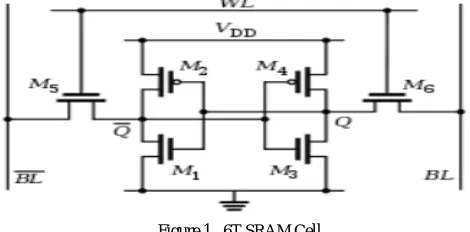
A. 6T SRAM CELL:
SRAM cell design depend upon the speed and size of the cell, SRAM cell should be sized as small as possible so large No of transistor can be fabricated on single chip, and we achieve high density in memory design. In 6T SRAM cell as shown in Fig. This SRAM consist of six transistors, two back to back cascaded inverter, and two NMOS pass transistor for access, a 6T SRAM cell has high speed, better noise immunity, and lesser area than other SRAM cell.
Each bit in an SRAM is stored on four transistors that form two cross coupled inverters. This storage cell has two stable states which are used to denote 0 and 1. Two additional access transistors serve to control the access to a storage cell during read and write operations. Access to the cell is enabled by the word line (WL in figure) which controls the two access transistors M5 and M6 which, in turn, control whether the cell should be connected to the bit lines: BL and ~BL. They are used to transfer data for both read and write operations [2].
ISSN(Online): 2320-9801 ISSN (Print): 2320-9798
I
nternational
J
ournal of
I
nnovative
R
esearch in
C
omputer
and
C
ommunication
E
ngineering
(An ISO 3297: 2007 Certified Organization) Website:www.ijircce.com
Vol. 5, Issue 1, January 2017
SRAM Cell Operation - Operation of the SRAM Cell can be categories into three different states: Sand by Mode circuit is in ideal mode, Read Mode when data has to be extracted, Write Mode when mode data has to be updated. The working of different mode can be explained:
Standby: If the word line is not asserted, the access transistors M5 and M6 disconnect the cell from the bit lines. The two cross coupled inverters formed by M1 – M4 will continue to reinforce each other as long as they are connected to the supply.
Reading: Assume that the content of the memory is a 1, stored at Q. The read operation is done by using the sense amplifiers that pull the data and produce the output. The row decoders and column decoders are used to select the appropriate cell or cells from which the data is to be read and are given to the sense amplifiers through transmission gate.
Writing: The start of a write cycle begins by applying the value to be written to the bit lines. If we wish to write a 0, we would apply a 0 to the bit lines, i.e. setting BL bar to 1 and BL to 0. A 1 is written by inverting the values of the bit lines. WL is then asserted and the value that is to be stored is latched in. Note that the reason this works is that the bit line input-drivers are designed to bemuch stronger than the relatively weak transistors in the cell itself, so that they can easily override the previous state of the cross-coupled inverters [2].
B. 4T SRAM CELL:
In the 4T SRAM cell, two NMOS transistors (M3 and M4) are used as pass transistors to access the cell and two PMOS transistors (M1 and M2) are used as drivers for the cell [3].
Figure2.4T SRAMcell
C. 5T SRAM CELL:
The5Tcellhasonlyoneaccesstransistor ‘N3’anda single bit line‘BL’,whichisshowninFigure3.Writingof‘1’or‘0’intothe5Tcellisperformed by driving the bit line to Vdd or ground respectively, while the word line is asserted at Vdd.Thewrite ability of the cellisensured by a different cellsizing strategy [4].
ISSN(Online): 2320-9801 ISSN (Print): 2320-9798
I
nternational
J
ournal of
I
nnovative
R
esearch in
C
omputer
and
C
ommunication
E
ngineering
(An ISO 3297: 2007 Certified Organization) Website:www.ijircce.com
Vol. 5, Issue 1, January 2017
D. 7T SRAM CELL:
7T SRAM cell is similar to the 6T SRAM along with an additional nMOS transistor as shown in figure 4. Alow overhead read/write assist circuitry is being proposed, which uses an additional transistor along with a floating ground as well as shown in figure 4. It proposes that the delay in case of writinga‘0’ is 29% faster than the conventional SRAM. Average power to writea‘0’has been reduced by 16% and power dissipationtowritea‘1’hasbeenreducedby54%.The trade off lies in larger are a consumption as it includes one extra transistor that controls the overall capacitances during the write and read operation [5].
Figure4. 7T SRAM cell
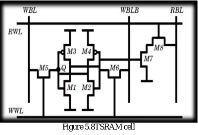
E. 8T SRAMCELL:
8T SRAM cell is shown in figure 5. This structure of SRAM is similar to 6T SRAM the two cross coupled inverter is used, and Two NMOS pass transistor is connected to the output of the inverter, inverter is connected to the WL which drives the pass transistor. In8TSRAMcell read noisemarginof theSRAM cellhas been enhanced by isolating the read and write operation. The 8TSRAM cell consists of 8transistors [6].
Figure 5.8TSRAM cell
IV.1BITSRAMCELLSTRUCTURE
ISSN(Online): 2320-9801 ISSN (Print): 2320-9798
I
nternational
J
ournal of
I
nnovative
R
esearch in
C
omputer
and
C
ommunication
E
ngineering
(An ISO 3297: 2007 Certified Organization) Website:www.ijircce.com
Vol. 5, Issue 1, January 2017
Figure 6. 1 bit SRAM cell structure
A. WRITE DRIVER:
The function of the SRAM write driver is to write input data to the bit lines when Write Enable (WE) signal is enabled; otherwise the data is not written onto the bit lines. Only one write driver is needed for each SRAM column. The schematic of the write driver circuit is shown in Figure 7 [7].
Figure7.WriteDriverCircuit
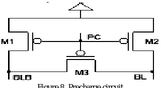
B. PRECHARGE CIRCUIT:
The f u n c t i o n of the precharge circuit in the SRAM array is to charge the Bit Line(BL) and Bit Line Bar (BLB)to VDD. The schematic of the precharge circuit for the SRAM array is shown in Fig8.ThetransistorM1andM2willprechargethe bit lines while the transistor M3willequalizethemto ensure both bitlines within a pair are at the same Potential before the cellis read [7].
Figure 8. Precharge circuit
C. ROW DECODER:
Address decoder is used to decode the given input address and to enable a particular word line (WL). In particular 2:4 dynamic NAND CMOS decoder is used [7].
Precharge circuit
Cell array
Write driver
Sense amplifier
Row decoder
ISSN(Online): 2320-9801 ISSN (Print): 2320-9798
I
nternational
J
ournal of
I
nnovative
R
esearch in
C
omputer
and
C
ommunication
E
ngineering
(An ISO 3297: 2007 Certified Organization) Website:www.ijircce.com
Vol. 5, Issue 1, January 2017
Figure 9. Row decoder
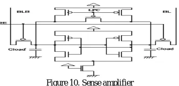
D. SENSE AMPLIFIER:
The function of SRAM cell in Sense amplifiers (SA) is sensing signal from BLB and BL. Sense amplifier is an important component in memory design. One of the major issues in the design of SRAMs is the speed of read operation. SA is present in every column of SRAM array. The read operation begins by precharging and equalizing both the bit lines, with simultaneously biasing the latch-type SA in the high-gain meta-stable region by precharging and equalizing its inputs. And then to read a particular word from the SRAM array, the corresponding row is selected by enabling the WL. Once a sufficient voltage difference is built between the bit lines, the SA is enabled by read enable (RE) signal. The SA will sense which bit line is heading towards high voltage and which bit line is heading towards ground potential and then a full voltage swing is obtained at the output [7].
Figure 10. Sense amplifier
V. SIMULATIONRESULTS
The following configuration of SRAM arrays were designed and analyzed using the Standard 6T SRAM Cell. Various configuration of SRAM structure were simulated using LTSPICE software in 45nm CMOS technologies. The functionality Write/read operation of 1*1 (1 bit) 6T SRAM cell in 45nm technology is shown in Figure 11 & 12. Following are the signals used in the simulation results: ‘pc’ corresponds to PC signal given to the Precharge Circuits; ‘wl’ corresponds to the WL signal of row in the SRAM array. This is the output of inverting buffer circuit; ‘we’ corresponds to the write enable signal given to the write driver circuits; ‘di’ correspond to input data bits; ‘lpc’ corresponds to the Precharge signal given to the Local Precharge circuits; ‘re’ corresponds to the read enable signal given to the sense amplifier circuits; ‘q’ correspond to storage node Q, ‘q1’ correspond to storage node QB of the SRAM.
ISSN(Online): 2320-9801 ISSN (Print): 2320-9798
I
nternational
J
ournal of
I
nnovative
R
esearch in
C
omputer
and
C
ommunication
E
ngineering
(An ISO 3297: 2007 Certified Organization) Website:www.ijircce.com
Vol. 5, Issue 1, January 2017
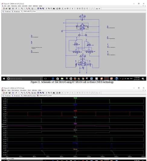
Figure 11. Schematic of 1bit SRAM using 6T SRAM cell in 45nm CMOS technology
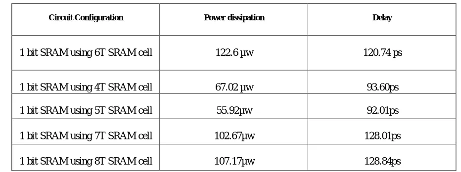
Figure 12. 1*1Write /read operation of 6T SRAM cell in 45nm CMOS technology
ISSN(Online): 2320-9801 ISSN (Print): 2320-9798
I
nternational
J
ournal of
I
nnovative
R
esearch in
C
omputer
and
C
ommunication
E
ngineering
(An ISO 3297: 2007 Certified Organization) Website:www.ijircce.com
Vol. 5, Issue 1, January 2017
Power = ID avg * VDD
Power dissipation and delay of different configure of 1 bit SRAM using different SRAM cells in 45nm CMOS technology result shown in table 1.
Table 1. Calculation of power dissipation and delay
Circuit Configuration Power dissipation Delay
1 bit SRAM using 6T SRAM cell 122.6 µw 120.74 ps
1 bit SRAM using 4T SRAM cell 67.02 µw 93.60ps
1 bit SRAM using 5T SRAM cell 55.92µw 92.01ps
1 bit SRAM using 7T SRAM cell 102.67µw 128.01ps
1 bit SRAM using 8T SRAM cell 107.17µw 128.84ps
VI.CONCLUSIONANDFUTUREWORK
1 bit SRAM cell using different n-T cells is designed in 45nm CMOS technology. The comparative results are given in Table 1 which shows that the power dissipation and delay are minimum for 5T and 4T SRAM Cells and maximum for 6T, 8T and 7T SRAM Cells respectively. The results can be used to select SRAM cell topology to design and fabricate memory chips which is best suitable for different type of application. We can design 4*4(16 bit), 16*16(256 bit), 32*32(1 Mb) SRAM cell in 45nm CMOS technology.
REFERENCES
1. KirtiBushanBawa, Dr. Sukhwinder Singh, “A Comparative Study of 6T, 8T and 9T SRAM Cell”, International Journal of Advanced Engineering Research and Technology (IJAERT), Volume 3, Issue 6, pp. 206-209, 2015.
2. VikasSingariya, D. K. Mishra, “Comparison of Various n-T SRAM Cell for Improvement of Power, Speed and SNM”, International Journal of Digital
Application & Contemporary research, Volume 2, Issue 12, 2014.
3. Kapil R. Joshi1, Prof. Mehul L. Patel, “Design and Analysis of a New Load less 4T SRAM Cell with 32nm CMOS Technology”, International Journal of
Advance Engineering and Research Development, Volume 2, Issue 5, pp. 901-906, 2015.
4. G. Boopathi Raja, M. Madheswaran, “Design and Analysis of 5-T SRAM Cell in 32nm CMOS and CNTFET Technologies”, International Journal of Electronics and Electrical Engineering, Vol. 1, pp. 256-261, 2013.
5. MedhaChhillar, Geeta Yadav, and Neeraj Kr. Shukla, “Average and Static Power Analysis of a 6T and 7T SRAM Bit-Cell at 180nm, 90nm, and 45nm
CMOS Technology for a High Speed SRAMs”, Association of Computer Electronics and Electrical Engineers, 2013.
6. Mrs. Sangeeta Singh, “Calculation of Performance Parameters of Different SRAMs”, International Journal of Advanced Research in Electronics and Communication Engineering (IJARECE), Volume 2, Issue 10, pp. 817-820, 2013.
7. K. Sreevani, D. Sankara Reddy, “DESIGN AND ANALYSIS OF 1KB 6T SRAM CELL IN DEEP SUBMICRON CMOS TECHNOLOGIES”,
INTERNATIONAL JOURNAL OF EMERGING TRENDS IN TECHNOLOGY AND SCIENCES, VOLUME-05, ISSUE-03, pp. 431-435, 2015.
8. S.Divyapriya, Dr. P.Ramamoorthy, “DESIGN AND ANALYSIS OF SRAM ARRAY STRUCTURES”, International Journal of Computer Science and
Mobile Computing, Vol. 3, Issue. 5, pp.515 – 522, 2014.
9. Yinhui Chen, Zhiyuan Yu, Haiqing Nan, and Ken Choi, “Ultralow Power SRAM Design in Near Threshold Region using 45nm CMOS Technology ”,
Illinois institute of technology, IL USA,©IEEE, 2011.
10. Preeti S Bellerimatha and R. M Banakarb, “Implementation of 16X16 SRAM Memory Array using 180nm Technology ”, International Journal of Current Engineering and Technology, pp. 288-292, 2013.
11. Shyam AKASHE, Sushil BHUSHAN and Sanjay SHARMA, “High Density and Low Leakage Current Based 5T SRAM Cell Using 45 nm Technology”,
ROMANIAN JOURNAL OF INFORMATION SCIENCE AND TECHNOLOGY, Volume 15, pp. 155–168, 2012.