Scaled Discrete Cosine Transform (DCT)
using AAN Algorithm on FPGA
Rahul R. Bendale 1, Prof. Vijay L. Agrawal 2
M.E. Student, Department of Electronics and Telecommunication Engineering, HVPM College of Engineering,
Amravati, Maharashtra, India1
Associate Professor, Department of Electronics and Telecommunication Engineering, HVPM College of Engineering,
Amravati, Maharashtra, India2
ABSTRACT: THE High Efficiency Video Coding (HEVC) standard is the modern video coding standard of the Video
Coding Experts Group and the Moving Picture Experts Group (MPEG).The discrete cosine transform (DCT), has become an uttermost important transform technique for image, audio and video signal processing applications for its utility and its supporting standards such as Joint Photographic Experts Group (JPEG), Moving Picture Experts Group (MPEG).The DCT characteristics make it perfectly suitable for image compression techniques and algorithms. Spatial data redundancies get reduced to larger extent by using DCT mostly in two-dimensional data. Therefore, For compression purpose of video coder JPEG and MPEG DCT is usefull.DCT soft core unit are used to perform the Discrete Cosine Transform (DCT) by using two dimensional eight x eight point DCT for the clock cycle with period of total sixty four clock cycles in an pipelined trending manner.
In following paper we presents a recent approach with error free architecture for most fastest implementation of an eight x eight two-Dimensional Discrete Cosine Transform, Multiplication-free nature, the mapping scheme used in this algorithm, eliminates most of computational and quantization errors also forms short-word-length and results in high-speed-design. High speed and high throughput is achieved through bit-serial and bit-parallel architecture along with pipelining. Multiplier accumulators in the DCT architecture have been designed with Distributed Arithmetic. Reduction in required area by elimination of the parallel multipliers by using distributed Arithmetic. Furthermore, a very high-speed operation can be achieved because by path formed in place of adders instead of multipliers. Architecture adequately implemented using descriptive language VHDL. For the realization of both implementations Virtex5 FPGA of Xilinx has been used.
KEYWORDS: High Efficiency Video Coding (HEVC), discrete cosine transform (DCT), FPGA, Virtex 5, Xilinx,
Matlab
I. INTRODUCTION
Discrete cosine transform (DCT's) are the most widely used transforms in the signal processing of digital image, video data, especially in the coding for compression algorithms. In video coding application applications, a two-dimensional DCT on small input sizes eight x eight is used. A digital unit called DCT soft core developed to perform the Discrete Cosine Transform (DCT). It performs two dimensional eight x eight point DCT for the period of 64 clock cycles in pipelined trending mode. Pipelined mode reduces the number of clock cycles required. To minimize the amount of calculations, the Arai, Agui, and Nakajama 8-point DCT algorithm is used.
II. DISCRETE COSINE TRANSFORM (DCT)
DESIGN FEATURES
For transforming data into a suitable format that should be easily compressed implemented a DCT. The DCT characteristics make it perfectly suited for image compression algorithms. DCT removes spatial data redundancies in two-dimensional data. Therefore, DCT is employed in standard image formats like JPEG and MPEG standards of compression procedures. In this, the two-dimensional DCT transforms associate n x n input data inform of array of n x n size result array. First of all the n-point DCT transforms the columns, so it transforms the rows. Calculation of 8-point DCT is done by using following equations _
(0) = 1
√8 ( ), ( ) =
1
2 ( )
(2 + 1)
16 , = 1,2, . . ,7
In above equation Y (k) = kth coefficient of DCT
The input array of size eight by eight image information block of integers in the range from 0 to 255. To reduce of the redundancy in the input information data block the mean value=128 is subtracted from input data Before the DCT calculation. The implemented DCT core can calculate input data in range –128 to 127 as well. Then the mean value 128 is not subtracted. Further the DCT is calculation, to concentrate the high important information into a less number of DCT results the data can be reduced, leaving the remaining coefficients equal to zero. Finally calculated image quantized energy is mostly quantized in a few DCT coefficients.
As in Comparison between the Discrete Fourier Transform & the DCT, DCT has the following advantages:
1. High image energy compaction
2. Lower blocking artifacts-
3. Real data coefficients and arithmetic only
4. Effective DCT algorithm
The Arai, Agui, and Nakajama 8-point DCT algorithm results in minimization of the quantity of calculations. The numbers of calculations done in algorithm are as following:
for i in 0 to 7 loop
y(i) = sa(i) * s(i) * 4.0; end loop;
In above loops a(i), y(i) are input and output data; m1 = cos (p / 4.0);
m2 = cos (p * 3/8);
m3 = cos(p/8) - cos(p*3/8); m4 = cos(p*/8) + cos(p*3/8);
The number of multiplications reduced to only 13 multiplies in this algorithm.
Pipelined computations
The input information data of 8x8 array sizes are feed in data by data wise with the period similar to the clock period. The output information data arrays are computed at output in the same way. Time margin (thresholds) between information data arrays can be absent, High maximum clock frequency of the DCT core is achieved because of the pipelined fashion calculations. For calculations of 64 word arrays clock period equal to 64 clock cycles is required. The input data and output data have the normal order.
Minimized hardware cost
Due to resource sharing the hardware required is very much less in volume. The multipliers number less and are equal to 4. Scaled output results require much less multiplier numbers and is equals to 2. The intermediate data are stored and transposed using the FIFO buffers
III. INTERFACE
Symbol
Figure1 shows DCT_AAN core symbol.
Fig 1. DCT_AAN core symbol.
Signal description
The descriptions of the core signals are represented in the TABLE I.
b0=a(0) + a(7); b1=a(1)+a(6); b2=a(3) - a(4); b3=a(1) - a(6);
b4=a(2) + a(5); b5=a(3) +a(4); b6=a(2) - a(5); b7=a(0) - a(7);
c0=b0 + b5; c1=b1 - b4; c2=b2 + b6; c3=b1+b4;
c4=b0 - b5; c5=b3 +b7; c6=b3 + b6; c7=b7;
d0=c0 + c3; d1=c0 - c3; d2=c2; d3=c1+c4;
d4=c2 - c5; d5=c4; d6=c5; d7=c6; d8=c7;
e0=d0; e1=d1; e2=m3*d2; e3=m1*d7;
e4=m4*d6; e5=d5; e6=m1*d3; e7=m2*d4; e8=d8;
f0=e0; f1=e1; f2=e5+e6; f3=e5 - e6;
f4=e3 +e8; f5=e8 - e3; f6=e2+e7; f7=e4+e7;
sa(0)=f0; sa(1)=f4+ f7; sa(2)=f2; sa(3)= f5 - f6;
TABLE I. DCT_AAN core signal description
Signal TYPE DESCRIPTION
CLK Input Global clock
RST Input Global reset
START Input DCT start
EN Input Clock enable
DATAIN[7:0] Input Input data
DATA_OUT[15:0] Output Output data
READY Output Result ready strobe
Data Format
Two's complemented 8 bit wide integers are Input data. The generic constant signed or unsigned iw d_signed. For unsigned, the mean value 128 is subtracted from all data.
Core Interconnection
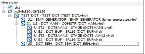
Digital circuitry is inherently hierarchical. Logic gates in digital circuitry is made up of transistors, flip-flops and latches are made up of logic gates, and more complex circuits are made up of latches and flip-flops and so on. The design in a structural description proceeds in a similar bottom up fashion.
Fig 2. Core interconnection
The advantage of this approach is the reusability of different logic modules. _ Fig. 2 Core interconnection Digital logic circuitry also get reflected in the layout phase of the design shown in figure-2 the components like INPUT_FRAME_BUFFER, OUTPUT_FRAME_BUFFER and, DCT_AAN _ Fig. 3
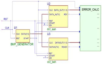
IV. TEST BENCH
The test bench is a VHDL module in which the unit under test (UUT) has been instantiated, together with pattern generators that are to be applied to the inputs of the model during simulation. Graphical displays and/or response monitors are part of the test bench. The test bench is documented to identify the goals and sequential activity that will be observed during simulation (e.g., "Testing the opcodes"). If design is formed as architecture of multiple modules, each must be verified separately, beginning with lower levels of the design hierarchy, then the integrated design must be tested to verify that the interaction among modules done correctly or not.
Fig 4. Test bench structure
In this case, the test architecture must describe the functional features of each module and the process by which they will be tested, but the plan must also specify how the aggregate is to be tested. Figure 4 shows VHDL test bench is
created and written for simulating it
For generatation of dataflow of testing arrays Component BMP_GENERATOR is used. There is Parallel processing of DCT_AAN and the reference instance DCT_BEH running in parallel to the source BMP_GNERATOR. The Behavioral model of the DCT processor is DCT_BEH. To calculate differences in the output data of DCT_AAN and DCT_BEH instant ERROR_CALC generated. Result of two signal subtraction is ERROR, sum of squared errors calculated for a single data arrays is SERROR, and QUADMEAN is the resulting mean square error value for the current data array.
V. RESULTS
Behavioral description of RTL
(a)
(b)
(c)
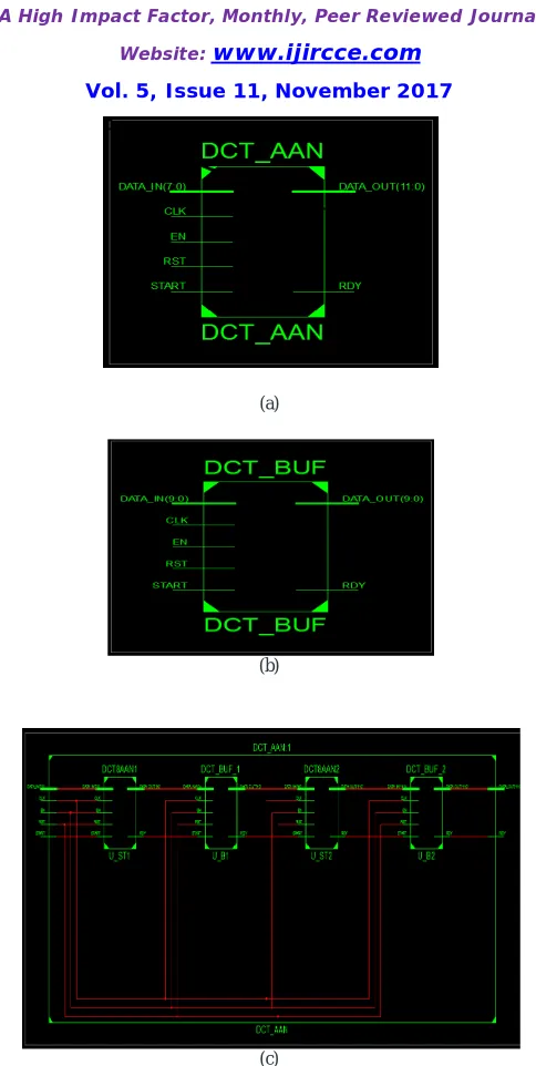
Fig 5. RTL schematic of (a) DCT_AAN component (b) DCT_BUFFER component and (c) top block DCT component
Figure 5 shows the RTL schematic of vital sub-blocks of the DCT project top module DCT_AAN. Each of the individual buffer and 8x8 dct components is a .ngr file and gives details of RTL logic as shown in figure 5 (a) and (b). For interconnecting each of cores the complete module designed is synthesized using file DCt_AAN.ngr.
Device utilization
The key architectural characteristics of the DCT-core were summarized earlier.
The Real time resources utilization of the selected target device by the designed modules is now presented here. They are being synthesized by Xilinx’s ISE design Suite 14.5 EDA tool and created a web file of Design Summary. TABLE II. Device utilization summary of DCT_AAN component out of 32 available on the board.
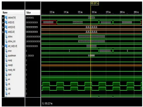
Simulation Waveform
The simulation waveform generated for the written and loaded test code is shown in figure 6. For easy verification of results the console data is printed by test bench. The console window of ISim snapshot is shown there.
Fig 6. Simulation waveform for written test bench
Description of simulation data is explained here:
Component BMP_GENERATOR generates the dataflow of testing arrays. There are two modes one mode generates predefined arrays, another mode does randomized ones. The two instances DCT_AAN and the reference instance DCT_BEH are tuned in parallel to the source BMP_GNERATOR. Behavioral model of the DCT processor is DCT_BEH. Resultant is 2-Dimensional DCT using the floating point. Its results are rounded to 12 bits. It’s standard model.
the array is QUADMEAN.
VI. FEATURES
Key features
More than 100 MHz sampling frequency, 64-cycle calculation period,
8-bit input data, 11-bit coefficients, 12 – bit results,
Pipelined mode,
Latent delay from input to output is 132 clock cycles,
Structure optimized for Xilinx Virtex_, Spartan_ FPGA devices.
Approximately 330 CLBs and 4 DSP48E in Virtex-5 device,2 DSP48E when the scaled output data mode is
used,
Minimized hardware cost: Due to resource sharing the hardware required is very much less in volume. The
multipliers number less and are equal to 4. Scaled output results require much less multiplier numbers and is equals to 2.
VII. CONCLUSIONS
The algebraic integer based on the Arai, Agui, and Nakajima (AAN) algorithm is used to reduce the computational complexity. Introduced an encoding scheme for the compression of the image which provides the low complexity architecture based on 8-point Arai algorithm. For reducing the size of the data sent i.e. image compression, to compute 2-D DCT with scaled output mode which effectively reduces the overall arithmetic and multiplication operations. This method is fast and provided the low complexity.
REFERENCES
[1] Arcangelo Ranieri Bruna,Fausto Galvan, Giovanni Puglisi, and Sebastiano Battiato,“ First Quantization Matrix Estimation From Double Compressed JPEG Images,” IEEE Transactions On Information Forensics And Security, Vol. 9, No. 8,pp, 1299-1310, August 2014. [2] Hamdy M. Mousa, Mostafa A. Ahmad, and Ashraf B. El-Sisi,“ Image Compression Ratio Enhancement Based on Conformal Mapping ,”
978-1-4799-0080-0/13,pp 280-285,IEEE 2013.
[3] Arjuna Madanayake, Renato J. Cintra, , Denis Onen, Vassil S. Dimitrov, Nilanka Rajapaksha, L. T. Bruton, and Amila Edirisuriya, “A Row-Parallel 8×8 2-D DCT Architecture Using Algebraic Integer-Based Exact Computation”, IEEE Transactions On Circuits And Systems For Video Technology, Vol. 22, No. 6, PP. 915-929,June 2012.
[4] Arai, Y., Agui, T., and Nakajima, M.: ‘A fast DCT-SQ scheme for images’, Trans. IEICE, 1988, E71, (11), pp. 1095–1097
[5] H. L. P. Arjuna Madanayake , R. J. Cintra , D. Onen , V. S. Dimitrov and L. T. Bruton, “Algebraic Integer based 8×8 2-D DCT Architecture for Digital Video Processing”, 978-1-4244-9474-3/11,PP. 1247-1250,IEEE 2011.
[6] Hatim Anas, Said Belkouch, M. El Aakif and Noureddine Chabini, “FPGA Implementation of A Pipelined 2D-DCT and Simplified Quantization for Real-Time Applications”, 978-1-61284-732-0/11/$, IEEE 2010.
[7] Yunqing Ye, Shuying Cheng “Implementation of 2D-DCT Based on FPGA with Verilog HDL”. Electronics and Signal Processing, LNEE 97, pp.633-639.
[8] Ruan, S.J ,Sun, C.C.,Heyne, B, Goetze, J ‘Low-power and high-quality Cordic-based Loeffler DCT for signal processing’ IET Circuits Devices Syst. 1(6), 453-461 (2007).
[9] Khayatzadeh, A., Shahhoseini, H.S., Naderi, M ‘Systolic Cordic Dct: An Effective Method Processing and its Applications’, vol.2, pp. 193-196 (2003).