Design and Performance of Microwave Components for ECH and
ECE Applications at General Atomics
James Anderson*, John Doane, Charles Moeller, Howard Grunloh, Raymond O’Neill, Michael Brookman, Matthew Smiley, and David Su
General Atomics, San Diego, CA, 92121, USA
Abstract. This paper provides an overview of high power components for the application of Electron Cyclotron Heating transmission lines, and broadband devices for Electron Cyclotron Emission detection systems. The unique fabrication and assembly challenges are discussed, particularly in the context of ITER. The ITER ECH system will require robust, vacuum-compatible components such as polarizers, dummy loads, and switches that are sufficiently cooled to withstand 1 MW for 3,600 seconds. These elements, along with overmoded corrugated waveguide, are necessary to form transmission lines with efficiencies of 90%, and 90% transmitted HE11 mode purity. Recent high power test results are summarized and scaled from the 63.5 mm internal diameter design to the 50 mm diameter version that will be used for ITER. Elements designed for Electron Cyclotron Emission detection and reflectometry systems are discussed, such as frequency filters and polarization rotators. The large frequency operating range of corrugated waveguide is exploited for such applications. The application of additive manufacturing technology towards both low and high power components is considered as a promising new area of development.
1 Overview
Microwave technology for fusion devices has evolved considerably over the past several decades. Experience gained from the practical application of electron cyclotron heating (ECH) systems such as at DIII-D, KSTAR, JT-60, NIFS, and EAST has led to steady improvements along with numerous innovations. While development of components has advanced through sometimes painful trial and error, reliability has gradually increased with lessons learned during the accumulation of operational hours on EC systems. As the ITER project looms, a robust microwave industry, spurred on by shared knowledge and recurring interaction, is more essential than ever.
General Atomics (GA) began design and production of high power, high frequency transmission line components in the early 1990s in support of the DIII-D ECH program for the US DOE. Specified for 110 GHz at 1 MW, transmission lines of 31.75 mm ID corrugated waveguide were fabricated, installed and operated at DIII-D. Currently DIII-D’s ECH systems include eight 90-meter transmission lines. GA has since provided numerous full-transmission line sets of components to a number of tokamak devices over the world. These components include corrugated waveguide, miter bends, polarizers, power monitors, waveguide switches, dummy loads, expansion units, pumping tees, tapers, DC-breaks, and gate valves.
Transmission lines for fusion applications can be divided into high power such as Electron Cyclotron Heating and Current Drive, and low power such as
Electron Cyclotron Emission diagnostic systems. As will be discussed in this review of microwave components and update on the state-of-the-art, each application has its own set of unique design criteria. A final section on additive manufacturing discusses a tantalizing future area of exploration.
2
Review of ECH Components
Applications such as ECH, where power levels can exceed 1 MW, present formidable challenges for component design and fabrication. As microwave output from gyrotron sources has increased both in terms of peak power and pulse length, the design emphasis has been placed firmly on maximizing transmission efficiency and minimizing mode conversion. Modern gyrotrons for ITER’s ECH system, for example, are intended to produce 1 MW for over 3600 s [1]. Factory acceptance tests of these gyrotrons have demonstrated 1 MW for 300 s [2], and 0.9 MW for 500 s [3]. Under such conditions, scaled measurements from QST’s gyrotron facility in Naka, Japan [4], suggest that over 512 W/m of heating will be dissipated for the HE11 mode supported in 6061-T6
aluminium alloy corrugated waveguide of 50 mm diameter at 170 GHz far from a miter bend. Within the approximately 1 m decay length for higher order modes at a miter bend, power absorption increases by 4 to 5 times. Therefore even though the HE11 mode is very low loss
Furthermore, ECH transmission lines generally require a high purity output mode in order to reduce added loading from stray radiation. For ITER, the output mode purity must be greater than 90% HE11 [5]. (For reference,
the ECH transmission lines at DIII-D are generally around 90% HE11 [6].) As a result of these strict requirements, as
well as demands from other high purity ECH systems, manufacturing tolerances on microwave components have become extremely tight. This creates a significant challenge in terms of fabrication, not to mention maintaining adequate quality control processes.
GA is currently ramping up its production capabilities for the considerable amount of waveguide components necessary for ITER. As part of this process, GA has supplied 63.5 mm and 50 mm 170 GHz corrugated waveguide to several high power test facilities. GA has also designed, built, and tested many prototype components that may be used for the ITER ECH transmission line.
2.1. Corrugated Waveguide
Fabricating extended sections of corrugated waveguide over half a meter in length generally requires special tooling. At GA, equipment has been developed to produce corrugated waveguide in lengths up to 2.1 m, although techniques have been developed to make even longer waveguide assemblies. The corrugation machines are adaptable enough to accommodate diameters from 31.75 mm up to 88.9 mm in materials such as aluminium, copper, and stainless steel. Corrugation of a full 2.1m section can take as little as 30 minutes, although in practice this step is just one of many, adding up to multiple man-hours.
2.1.1 Ex-vessel Waveguide
As described in [7], the 4.2 m water-cooled aluminium corrugated waveguide assembly meets ITER tolerances. In 2015, this component was installed and tested at the QST high power gyrotron facility at 450 kW over 300 seconds. The results revealed double the expected power absorption compared to previous measurements, although this was due to unexpected reflections elsewhere in the transmission line [8].
The waveguide was made in 63.5 mm diameter rather than the 50 mm diameter in ITER’s current specification, yet the experiments suggested the waveguide is suitable for an ITER ECH transmission line. Work is underway to model and analyse a scaled water-cooled corrugated waveguide design at 50 mm diameter. Generally the attenuation losses scale as the inverse of the radius cubed, so the expected absorption becomes roughly twice that measured previously [4]. However, this increase is not expected to impact the approach to active waveguide cooling.
Uncooled regions where joint couplings are necessary are important to analyze. Couplings can be designed to have significant heat capacity as well as much higher thermal conductance than regular waveguide because of the larger cross section. If the coupling is about 20 cm
long and has an OD of about 10 cm, its heat capacity plus the heat capacity of the waveguide is about 2850 J/K. If the waveguide absorbs 100 W in the 20 cm length, then in a 3600 second pulse with radial conduction to the coupling, the average temperature rise of the coupling and waveguide underneath would be about 126 C. Axial conduction through the neighboring walls to the nearby cooling channels will reduce this heating further, so there should be no need to cool the couplings.
2.1.2 In-vessel Waveguide
Inside a fusion device, the environment generally becomes quite severe, not to mention unpredictable and chaotic. Ultra-high vacuum conditions coupled with the presence of energetic particles creates a different set of limitations on transmission line design, both in terms of cooling approach and material selection. In addition, the region within the bio-shield is not typically accessible, so reliability becomes an important factor, along with the development of proper installation and assembly procedures.
Informed by experience from operating ECH launcher components at DIII-D, General Atomics has developed a number of recent in-vessel waveguide components for tokamaks, including JT-60SA. At KSTAR, the launcher region was instrumented with a number of sensors. The measurements indicated thermal equilibrium was reached for the in-vessel water-cooled launcher mirrors during a 60.5 s gyrotron pulse at 800 kW [9], an encouraging result for long-pulse operation.
A 1.5 m stainless steel corrugated waveguide was built by GA as a prototype for launcher components at JT-60SA (Figure 1). A stainless steel sheath was welded to the outside to form a water-cooled jacket. The corrugations were plated with nickel in a sulfamate bath to reduce the resistivity at the metal surfaces. As revealed by looking at a sample with a scanning electron microscope (SEM), the process produced a uniform coating of nickel (Figure 2). The thickness ranged from 5 to 10 microns, several multiples of the skin depth. According to [10], the resistivity of electrolytic nickel plating is 8.6x10⁻⁶ ohm-cm, compared to 7.4e-5 ohm-cm
for 316 L stainless steel alloy. Since the attenuation is proportional to the square root of the resistivity, the amount of power absorption is reduced by a factor of 2.9 by applying the relatively inexpensive plating process.
Fig. 2. SEM images of nickel-plated stainless steel corrugations. The images show the uniformity of the plating process. The slight distortion of the corrugations occurred when the sample was cut.
A transmission line was constructed to test ECH components for the JT-60SA tokamak at QST. Recent experiments were conducted comparing power absorption in aluminium waveguide with both plated and unplated stainless steel waveguide using 20 s pulses from a 110 GHz gyrotron at 500 kW [11]. The measured temperature rise of a section of unplated stainless steel waveguide was around 2.5 times that of an aluminium section, which matches the theoretical value when accounting for the heat capacity of the materials. In a similar comparison, the nickel plated section had a slightly lower temperature rise than that of aluminium. The theoretical ratio is 0.9.
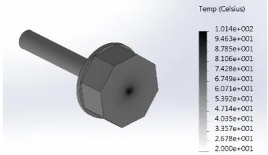
For the ITER reactor, in-vessel components are subject to a number of requirements which place constraints on design of corrugated waveguide intended for the equatorial and upper ECH launchers. Among these constraints are welds, which must be full-penetration at water/vacuum boundaries, and subject to 100 percent volumetric inspection using non-destructive examination (NDE) techniques. GA has contributed to the development of a conceptual design for a 2 m long, 50 mm inner diameter equatorial launcher corrugated waveguide, as shown in Figure 3. The component is nickel-plated stainless steel, with a welded outer water jacket. To improve the cooling uniformity around the circumference of the waveguide, two input channels are used with two return channels. The water connections are accessible at the non-vacuum side of the component. The number of fabrication steps make the assembly challenging, but within the capability of modern machining and welding techniques. Analysis of the design using ANSYS shows the water cooling approach is acceptable for 1.2 MW transmission at steady state conditions (Figure 4).
Fig. 3. Conceptual design of equatorial ECH launcher waveguide for ITER.
Fig. 4. Temperature distribution of the outer surface of the conceptual equatorial launcher waveguide. The most significant heating occurs at the non-cooled flange at the non-vacuum side, where the temperature rise is around 33 C. The water inlet temperature is 94.5 C.
2.2. Polarizers
Miter bends with rotatable grooved mirrors are often used for polarization control in ECH systems. Two miter bends (a linear polarization rotator and a circular polarizer) can produce the full range of polarization states, although it is possible to achieve some amount of polarization control with a single grooved mirror albeit with higher losses [12]. The design of a motorized 63.5 mm diameter polarizer miter pair for ITER is presented in [13], along with a generalized theory for predicting the ohmic losses of such components. Prototypes of these polarizers were tested under high power conditions (~350 kW over 500 s) at QST. Low power measurements and finite element analysis has shown the effectiveness of the design [14].
Adjusting to updated requirements, GA has developed an ITER polarizer design for 50 mm diameter. A steady-state analysis of the mirror design for 1.2 MW incident power at an input flow rate of 20 liters / min. indicates the cooling will be sufficient to limit the temperature rise at the mirror surface to around 120 C, even at the groove orientation with highest losses. The maximum amount of distortion is under 30 m over the surface.
Fig. 5. Temperature distribution for 50-mm polarizer.
A ferromagnetic fluid-based seal is used to enable smooth, rapid rotational motion of the mirror driven by a motor external to the vacuum. This type of seal, commonly found in the semiconductor industry, is considered to be highly reliable. To reduce impact of failure, it is possible to design a small secondary interspace between the seal and the primary vacuum. The interspace can be monitored for leaks, and may even provide an automatic isolation seal triggered by a pressure differential.
Since many ECH systems are now multi-frequency, there is an increased interest in broadband polarizers. For
100 um
5 um 5 um
5 um
example, KSTAR has gyrotrons which produce power at 105 and 140 GHz. By applying the theory as discussed in [13], it can be shown that GA’s polarizer pairs used for that system (originally designed for 140 GHz) have stable operating points over the full range of polarizations at 105 GHz. A recent set of polarizers produced for the upgrade at TCV are designed to operate at 82.6, 84, and 118 GHz. (These polarizers also required fast setting of mirror position, with a full 180 rotation of the mirror in 0.2 s.) Finally, there is recent consideration of making the ITER installation a dual-band system. Calculations show that the GA polarizer pair for ITER will produce the full polarization spectrum at both 104 and 170 GHz.
2.3 Dummy Loads
High power microwave dummy loads are essential for conditioning, testing, and commissioning gyrotron sources. The dummy load system developed at GA typically consists of three elements: a downtaper to 31.75 mm diameter, a waveguide attenuator, which absorbs most of the power, and a compact tank load which dissipates the remaining power. As described more fully in [15], the attenuator consists of a section of varying corrugation depths either in copper or CuCrZr copper alloy that converts the HE11 mode to a surface wave,
which has high attenuation. The advantage of this approach is that it has very low reflected power, relatively low water flow requirements, short time constants, no welds, and no rotating parts. The system has been used successfully at DIII-D, KSTAR, and EAST. Recently a prototype system has been built to handle 1.4 MW continuous power at 170 GHz for ITER (Figure 6). The waveguide attenuator was designed to absorb 85% of the power (1.2 MW) with the rest of the power (200 kW) collected in the tank. Around 80% absorption was measured in the waveguide attenuator during cold test. Although designed to transition from 63.5 mm waveguide, the system is easy to adapt to a 50 mm transmission line by replacing the taper in Figure 6(a).
(a) (b) (c)
Fig. 6. The downtaper (a), attenuator (b), and tank (c) elements of the dummy load system designed for ITER conditions.
During gyrotron conditioning, the load system installed at the EAST facility withstood 630 kW of power at 1 s. The pulse width was limited during the time since the attenuator was absorbing less of the total power than expected (60%, rather than 80%), raising concerns about overheating the tank load. Calculations of the load geometry based on ray tracing conclude that the power rating of the tank load is about 500 kW CW in the most favourable input polarization orientation, and 250 kW CW in the orthogonal orientation. Therefore it should be possible to condition the gyrotron using long pulses despite the 60% absorption. The lower-than-expected absorption of power in the waveguide attenuator could be due to low HE11 mode purity. While measurements
showed that the output mode purity from the gyrotron was around 90%, it is possible that the HE11 content is smaller
at the input of the load due to any misalignments in the transmission line between the gyrotron and load.
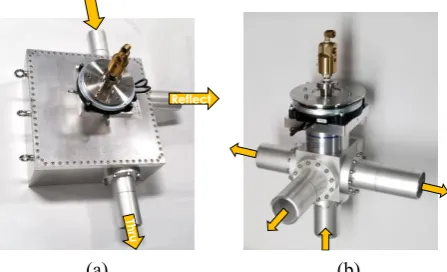
2.4 Switches
Waveguide switches are used in applications where microwave power is necessary at multiple locations. Alternatively they enable a facility with several gyrotrons to dump power into a single load. For example, a switch such as the one shown in Figure 7(a) can be used to switch ECH power between the equatorial and upper launchers at ITER. This motorized switch, which employs a rotating mirror, is designed for 1.4 MW at steady state. It is fairly compact to accommodate 300 mm spacing between waveguide centerlines of adjacent switches, and has few parts compared to other types of waveguide switches, which improves reliability. In addition, it has low consumption of water for cooling, ≤ 0.1 kg/s with <0.6 MPa total pressure drop. The switching time has been demonstrated to be as low as 0.6 seconds, which may be useful in certain mode suppression scenarios for ITER. (Another type of rotary switch, developed for the ITER Low Field Side Reflectometer, has switching speeds < 0.1 second). While it was originally designed for 63.5 mm diameter, the ECH unit is easily scaled to 50 mm since the heating conditions of the flat mirror will be less than that for the grooved mirrors of the polarizers discussed in the previous section.
(a) (b)
The rotary switch shown in Figure 7(a) has input and output ports in the same plane. An alternate configuration has output ports out of plane from the input port, such as the four port switch built for the TCV upgrade (Figure 7(b)). This particular approach allows for up to four different switching states. For vacuum applications, the assembly incorporates the same ferromagnetic fluid feedthrough as the polarizer. Overall, the rotary waveguide switches have proven to be robust, reliable, and inexpensive.
2.5 Transmission Line Diagnostics
Microwave power at the megawatt level has the potential to cause significant damage, in addition to posing an occupational safety hazard. It is not difficult to find instances of ECH power destroying sensitive equipment or disrupting delicate systems [16]. Such cases underline the importance of properly monitoring high power transmission lines. Moreover, it is often useful to have the ability to determine key transmission parameters such as power, polarization, frequency, and mode purity. This information may be used to determine problems with components in a microwave system, particularly the gyrotron. Often the signals from these devices are employed as safety interlocks.
GA has developed a number of different types of diagnostic components for corrugated transmission lines. As described in [17], two different diagnostics have been built and tested for measuring power in ECH transmission lines for ITER. A new power monitor miter bend using a CuCrZr mirror machined with small sampling holes was instrumented with a pair of diode detectors to indicate forward and reverse power of a 170 GHz signal produced by a gyrotron at the QST test facility. The power monitor miter bend provides instantaneous accurate power levels, as well as signal directionality. The signals from the sampling ports can also be used to determine frequency. An alternative is the calorimetric miter bend, which uses a CuCrZr mirror that is thermally isolated from the body of the miter bend. By measuring the temperature rise of the cooling water passing through the mirror, it is possible to determine the power in the transmission line. Such a device is not expensive. However, since it requires thermal equilibrium, it does not provide an instantaneous power measurement.
2.5.1 Inline Power and Polarization Monitor
A more simplified version of the power monitor miter bend is the inline power monitor, such as the one modelled in Figure 8. A calorimetry-based inline power monitor has been used at DIII-D, but since it was not placed far enough from miter bends and other sources of mode conversion, it has had limited success in providing accurate power measurements.
An updated inline power monitor, based on a gap-type pumpout port, uses diode detectors to provide instantaneous signals. The small gap allows a small amount of signal to leak out to the sampling ports. In its
simplest form, a diode detector at a single sampling port can be used as an indication of power. For a high mode purity system, the signal from this inline power monitor may provide a calibrated power measurement, assuming it is placed far enough from sources of mode conversion. Two opposing ports may be instrumented with diode detectors at 90 orientations. In such a configuration it is possible to use the device as a polarization discriminator. By instrumenting all four ports with detectors, it may be possible to collect information on the mode structure of the travelling wave, making for an effective technique for monitoring misalignments in the transmission line.
Fig. 8. Inline power monitor with multiple ports for polarization discrimination.
A lower cost option is the inline power monitor based on a single-hole design, rather than the gap-type approach. This version provides a monitor port with a coupling of around -70 dB, which is large enough for a diode detector to measure assuming 1 MW incident power. Although the device does not allow for instantaneous polarization comparison, it may be used in applications where a simple indicator of power (or frequency) is all that is required.
2.5.2 Mode-Sampling Miter Bend
For more detailed analysis of the mode structure in an overmoded transmission line, GA has designed a mode-sampling miter bend [18]. Sometimes referred to as a “leaky” miter bend, the mirror of this device contains many small signal-coupling holes. Polarization discrimination is enabled with a transition down to a standard waveguide orthomode transducer at the back of the leaky mirror. Alternatively, several mode couplers can be used, each coupler with its own diode detector. In this configuration it is possible to instantaneously collect calibrated power measurements of the HE11 mode, as well
as theLP11 odd and even modes commonly associated
with tilt and offsetmisalignments. A version of this mode sampling miter bend was built and instrumented for the ECH transmission lines at DIII-D for 110 GHz. A prototype has also been built for 170 GHz which may be used as a diagnostic on an ITER high power 63.5 mm diameter transmission line test bed. This leaky mirror design requires approximately 5,000 holes through the 1 mm thick plate, which must be leak tight.
3 Review of Diagnostic Components
Overmoded transmission lines play an important role in many low power applications as well, although the design of these components face a different set of challenges than
those intended for high power applications such as ECH. For example, plasma diagnostics like Electron Cyclotron Emission (ECE) detection systems and reflectometers require very wide operating bands. The emphasis is not on heat management or maintaining strict vacuum requirements, but rather on optimizing signal quality over a range of frequencies. Low loss is still essential.
3.1. Frequency Filters
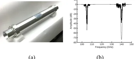
The ECH system at KSTAR is dual-frequency, with gyrotrons producing power at 105 GHz and 140 GHz. The ECE detection system is designed to operate over a band which encompasses those frequencies. GA has built several notch filters to protect the diagnostic’s sensitive electronics. The notch filters are made using a series of biaxial polystyrene sheets separated by thin spacer disks in a corrugated waveguide assembly. The assembly for two notches, as shown in Figure 9, is around 760 mm in length. The measured response showing the two notches is also shown. A similar notch filter was delivered to EAST, although with a single notch at 140 GHz.
(a) (b)
Fig. 9. Dual-notch filter for KSTAR ECE diagnostic in 63.5 mm corrugated waveguide (a). Measured frequency response near 105 GHz and 140 GHz (b).
A different type of frequency filter is planned as a protection element for the Low Field Side Reflectometer for ITER. For this system, which will operate from 30 to 165 GHz, it is necessary to have a low pass filter at 170 GHz. A diffraction grating was designed to replace the mirror of a miter bend (Figure 10). For frequencies below 170 GHz, the signal will reflect off the mirror at an angle equal to the angle of incidence. For higher frequencies, the power is reflected back into the input waveguide where it is attenuated within about a meter from the mirror. The grating is polarization sensitive, so two miter bends in orthogonal planes are necessary to protect the diagnostic for all possible incoming field orientations.
(a) (b)
Fig. 10. Diffraction grating reflector for 63.5 mm miter bend (a). Measured and theoretical frequency response near 170 GHz (b).
3.2. Polarization Rotators
Diagnostics using microwave signals typically rely on information gained from specific polarizations. In emission detectors and reflectometers, it is therefore advantageous to rotate linearly polarized signals, either on transmit or receive. One means of doing this is to use a three mirror polarization rotator configuration, such as shown Figure 11 for the EAST ECE system. In such an arrangement it is possible to achieve a full 90 rotation of polarization by mechanically rotating the assembly 45 around the axis of the input and output waveguide. A motorized version of the three-mirror polarization rotator using rotary joints has been designed for the ITER Low Field Side Reflectometer (LFSR) system.
Fig. 11. Polarization rotators for ECE diagnostic at EAST.
3.3. Broadband Waveguide
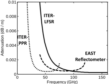
Microwave diagnostics such as radiometers and reflectometers operate with frequencies in the range of the electron cyclotron resonance and right hand cutoff, which can vary by 2-3 octaves in a tokamak plasma due to dependencies on density and magnetic field. Examples of recent or planned reflectometers are the 40-120 GHz reflectometer for EAST, the 15-75 GHz Plasma Position Reflectometer for ITER, and the 30-165 GHz LFSR for ITER. Such applications are ideal for corrugated waveguide, which maintains low ohmic loss in the HE11
mode over large frequency ranges. The calculated loss for the three diagnostic waveguide types is shown in Fig. 12 in 6061-T6 aluminium alloy (assuming 4x10⁻⁶ ohm-cm
resistivity and 30% roughness enhancement for surface resistance).
100 110 120 130 140 150 -80
-70 -60 -50 -40 -30 -20 -10 0 10
Frequency (GHz)
A
m
p
lit
u
d
e
(
d
B
)
155 160 165 170 175 180
-30 -25 -20 -15 -10 -5 0 5
Frequency (GHz)
A
m
p
lit
u
d
e
(
d
B
Fig. 12. Theoretical HE11 attenuation in 6061-T6
aluminium for ITER PPR waveguide (dotted), EAST reflectometer waveguide (dashed), and ITER LFSR waveguide (solid).
4 Additive Manufacturing
As the technology has advanced, additive manufacturing has played an increasing role in design and fabrication of microwave components. Although the process is primarily associated with plastic, the range of materials has expanded to include many different metals, including stainless steel, aluminium, and copper. While it is possible to procure metal-plated plastic microwave components from commercial sources specializing in additive manufacturing [19], examples may also be found of direct printing metallic waveguide structures using laser sintering [20]. At GA, additive manufacturing has been used to explore means of lowering fabrication costs, accelerating development of new components, and enhancing performance [21]. The research is divided into two areas: low power and high power microwave components.
4.1. Low Power Components
Many low power microwave applications make use of overmoded components which are fairly compact, such as elements used to transition to corrugated waveguide from fundamental rectangular waveguide. In applications where the volume of the part is within the build size of an additive manufacturing machine, it may be advantageous to print the part, since the turn-around time for a printed part is generally short compared to a machined or electroformed part. With additive manufacturing, it is therefore possible to establish a rapid prototyping development cycle for optimizing a design quickly at relatively low cost.
Direct Metal Laser Sintering (DMLS) has been found useful in making tapered corrugated horns with output apertures as large as 63.5 mm in diameter. While the individual layer thickness of parts produced from current DMLS machines is within the +/-25 m tolerance resulting from a conventional machining approach, the resolution of a geometry produced on a given layer of printed metal is around 350 m. As a result, the maximum frequency for such components is limited to around 100
GHz. For higher frequency components, plastic additive manufacturing processes such as PolyJet (15 m layer thickness, 40 m X/Y resolution) or projection stereolithography (SLA) (5 m layer thickness, 25 m X/Y resolution) are more effective. Commonly used electroless copper and nickel plating processes of plastic parts have been proven for coating the fine corrugations, even in difficult-to-access regions such as the throat of a corrugated horn. The metal plating produced by these processes is not as electrically conductive as electrolytic plating, but the applications for such low power components are usually not focused on minimizing ohmic loss.
A recent example of a 3D printed corrugated component is shown in Figure 13. The part, which represents a section of a transition from WR-6 to 63.5 mm diameter corrugated waveguide, was made by copper plating a corrugated geometry via SLA. Low power measurements of the assembly using the printed part was compared to the assembly using a machined version (in two sections). The resulting HE11 mode purity in both
instances was above 97%.
Fig. 13. Metal-plated corrugated section made via additive manufacturing used in assembly to transition from WR-6 to 63.5 mm corrugated waveguide at 140 GHz.
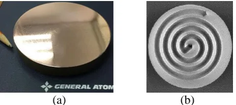
4.2. High Power Components
In the realm of high power microwaves, plastic parts are typically avoided, and metal printing processes such as DMLS are the default technology. The focus is no longer on rapid prototyping, but fabricating robust vacuum-qualified parts which can withstand high temperatures. One advantage that additive manufacturing offers in this scenario is its ability to incorporate conformal cooling channels. While it is possible to provide some amount of complexity to cooling in conventionally machined high power parts, the fabrication process often requires advanced assembly techniques such as brazing or electron beam welding which add technical risk. Additive manufacturing has an established capability of producing internal channels which are consistent with the geometry of the part, and can provide cooling to crucial regions that may be otherwise difficult to access.
0 50 100 150
0 0.002 0.004 0.006 0.008 0.01
Frequency (GHz)
A
tt
e
n
u
a
ti
o
n
(
d
B
/
m
) ITER-LFSR
ITER-PPR
EAST Reflectometer
Printed &
Plated
A flat copper mirror, such as one used in a typical overmoded miter bend, is currently being investigated at GA (Figure 14). Two sample mirrors representative of those used in a 63.5 mm diameter waveguide miter have been produced in commercially available DMLS copper alloy materials (C18200 CuCr and CuNi2SiCr). The mirror blocks have identical spiral-shaped cooling structures. This channel geometry is theoretically more efficient in terms of heat transfer than the straight cooling channels enabled by conventional machines for a miter mirror. The surfaces were polished to near mirror-quality (around 8 microinch Ra). No leaks were discovered when vacuum pumping on the mirror surfaces to 1x10⁻⁹ Pa/m3
-s. A static water pressure test was also applied to the cooling channels with 0.7 MPa. Nevertheless, a hot isostatic press (HIP) process was applied to further minimize porosity of the sintered copper alloy.
(a)
(b)
Fig. 14. 3D-printed copper mirror for a 63.5 mm miter bend (a), and X-ray image of spiral-shaped internal cooling channel (b).
Following the initial tests to verify the process, a finalized mirror made via DMLS is being planned which may be incorporated into the miter bend housing of a high power transmission line for testing.
This work was funded through internal research and development at General Atomics. The authors would like to acknowledge K. Sakamoto, K. Takahashi, Y. Oda, T. Kobayashi, R. Ikeda (QST), Y. Uemoto (MHI), M. Joung (NFRI), G. Wang (UCLA), L. Yong (ASIPP), T. Goodman (EPFL-SPC), M. Henderson (ITER-IO).
References
1. M. Henderson, “Status of the ITER EC system,” presented at US/EU/JA Workshop on RF Heating Tech., Santa Monica, CA, USA, Sep. 4-7, 2017.
2. K. Takahashi et al., “Development of ITER gyrotrons and equatorial launcher,” presented at US/EU/JA Workshop on RF Heating Tech., Santa Monica, CA, USA, Sep. 4-7, 2017.
3. T. Goodman et al., “FALCON test facility,” presented at US/EU/JA Workshop on RF Heating Tech., Santa Monica, CA, USA, Sep. 4-7, 2017.
4. J.P. Anderson et al., “Heating effects in overmoded corrugated waveguide for ITER,” J. Infr. MMW-THz Waves, 37, 1, 2016.
5. G. Hanson, “ITER ECH transmission line system update,” presented at US ECH Tech. Community Meeting, San Diego, USA, Feb. 6, 2017.
6. J. Lohr et al., “Performance history and upgrades for the DIII-D gyrotron complex,” presented at US ECH Tech. Community Meeting, Oak Ridge, TN, USA, May 8, 2014.
7. J.P. Anderson, et al., “High power testing of water-cooled waveguide for ITER-like ECH transmission lines,” Nucl. Fusion, 57, 5, 2017.
8. W. Bin et al., “Status of the high power matched load activity at IFP-CNR,” presented at US/EU/JA Workshop on RF Heating Tech., Santa Monica, CA, USA, Sep. 4-7, 2017.
9. M. Joung et al., “KSTAR ECH status and plan for high performance and steady-state operation,” presented at 22nd Conf. on RF Power in Plasmas, Aix-en-Provence, France, May 30 – June 2, 2017. 10. W.H. Safranek, Properties of Electrodeposited
Metals and Alloys, 2nd Ed., Amer. Electroplaters Soc., Dec. 1986.
11. T. Kobayashi et al., “Progress in ECRF system development and preparation for JT-60SA,” presented at US/EU/JA Workshop on RF Tech., Santa Monica, CA, USA, Sep. 4-7, 2017.
12. M. Saigusa et al., “Thermal analysis and ohmic loss estimation of polarizer for ITER ECCD system,” Fusion Eng. Des., 74, 2005.
13. J. Doane, H. Grunloh, W. Martin, and W. Wu, Fusion Eng. and Design, 102, 2016, pp. 99-107.
14. S. Jawla et al., “MIT program update,” presented at ECH Tech. Community Meeting, San Diego, USA, Feb. 6, 2017.
15. J.L. Doane, “Tests of compact dummy loads designed for 1 MW CW,” Proc. Of the 12th Joint Workshop on ECE and ECH, Aix-en-Provence, France, 13-16 May 2002, World Scientific, 2003.
16. J. Lohr et al., “Operating a multiple gyrotron system,” presented at US/EU/JA Workshop on RF Heating Tech., Sedona, AZ, USA, Sep. 22-24, 2014. 17. J. Doane, et al., “Power monitor miter bends for high-power microwave transmission,” Fusion Eng. And Design, 93, 2015.
18. C. Moeller et al., “Status of mode-selective ECH miter bend power monitor,” presented at US/EU/JA Workshop on RF Heating Tech., Santa Monica, CA, USA, Sep. 4-7, 2017.
19. www.swissto12.com
20. T. Horn et al., “Additively manufactured WR-10 copper waveguide,” presented at Int’l Vacuum Elect. Conf. (IVEC), Monterey, CA, USA, April 24-26, 2018.