Enhanced sensitivity with thickness optimization of ZnO based acetone sensor
Manish Deshwal & Anil Arora*Electronics and Communication Engineering Department, Thapar University Patiala, 147 004, India Received 18 August 2017; accepted 7 February 2018
Zinc oxide (ZnO) thin film based acetone gas sensor has been studied with variation of sensing layer thickness towards 500 ppm of acetone. The effect of thickness variation of the sensing layer on the structural, surface morphological, optical and gas sensing properties of ZnO thin film has been studied. A significant increase from 7.19 to 63 in the sensing response has been observed with bare ZnO thin film for the samples with an optimised thickness of 410 nm at an optimised operating temperature of 320 C. This study conducts the variations in structural, optical and the gas sensing characteristics while varying the thickness of ZnO based thin films for an acetone gas sensor. Further, the study concludes with an optimised thickness as 410 nm for an oxidizing gas.
Keywords: Acetone sensor, Thickness optimization, ZnO thin film 1 Introduction
In the recent times, comprehensive studies have been conducted for the solid state gas sensors for monitoring the environmental conditions, chemical processes, occupational health, safety and medical
devices1. Previously, the miniaturization of
semiconductor metal oxide based sensors had been widely exploited for low cost, fast response and
recovery times with ease of fabrication2-4. Up to now,
various semiconducting oxides like ZnO, SnO2, In2O3
and TiO2 have been utilized for the fabrication of solid
state gas sensors4,5. Zinc oxide (ZnO) is one of the
most versatile semiconductor materials which possesses a wide direct band gap of 3.37 eV at room
temperature6-8. It is having a variety of applications
including luminescence, acoustic, electrical devices
and solar cells9. ZnO thin films have been
substantially studied as a gas sensing metal oxide semiconducting layer due to its high stability, ease of fabrication, and high stoichiometry for various gases. There are numerous deposition techniques for fabrication of ZnO thin films which includes sol-gel process, pulsed laser deposition (PLD), RF/ DC sputtering, molecular beam epitaxy (MBE), and
chemical vapour deposition (CVD), spray pyrolysis10-15.
Sol-gel is one of the most reliable methods for fabrication of ZnO thin films due to its low cost, ease
of fabrication and multifaceted micro structures16-18.
Now days, acetone is being used in almost all the
chemical laboratories and industries which exhibits very adverse effects towards humans. Acetone either directly or indirectly if inhaled can cause severe damage to liver, lungs, kidneys and also have an
adverse effect on the central nervous system19. In the
present work, ZnO thin films have been studied for various thicknesses of 160 nm, 280 nm, 410 nm and 540 nm to find the optimum thickness such that the sensor exhibits high sensitivity, quick response and recovery times. The optimise thickness comes out to be 410 nm which shows the highest sensing response of 63. The present study proposes for the optimum thickness for an acetone sensor which is further related with high degree of crystallization and larger surface areas.
2 Experimental
The chemical reagents used in this experiment are of analytical grade with distilled water having
resistivity of 18.2 MΩcm-1. The zinc acetate
dehydrate Zn(CH3COO)2·2H2O is dissolved with
ethanol to prepare 0.1 M sol. Subsequently, monoethanolamine (MEA) is added drop wise in distinct amount as stabilising agent followed by refluxing of solution at 80 °C for 20 min. The prefabricated inter digitated electrodes (IDE) over
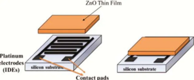
SiO2/Si substrates (as shown in Fig. 1(a)) are
ultrasonically cleaned in acetone for 30 min followed bydesiccation in hot air oven. ZnO thin films has been coated using spin coating technique over the prefabricated IDE’s at 2500 rpm for 20 s and repeated
—————
till the desired thickness is achieved with subsequent baking at 300 °C for 5 min after each coat (as shown in Fig. 1(b)). The thin films are annealed at 650 °C for 5 h in a closed and controlled environment for decomposition and oxidation of the precursors of the solution. The samples with thicknesses 160 nm, 280 nm, 410 nm and 540 nm are prepared with repetition of spin coats and termed as samples S1, S2, S3 and S4, respectively. The optical, structural and surface morphological characteristics for the samples have been carried out using UV-visible spectrophotometer, X-ray diffraction (XRD) and field emission scanning electron microscope (FESEM). For UV-visible spectrophotometer the samples are prepared over quartz substrates with same conditions. For gas sensing characterization processes, the films are deposited on the IDE patterned silicon substrate with same parameters. An indigenously developed gas calibrator and test system (GCTS) consisting of a glass bell jar, thermocouple, heating element, temperature controller and the contact pins connected to digital multimeter (Keithley 2002) is used for the data acquisition as shown in Fig. 2. Thermal volatization of liquid acetone is used for preparation of vapours which were inserted in the chamber through calibrated leaks with desired concentration of 500 ppm in atmospheric conditions. The gas is
injected through the inlet nozzle and suctioned using a rotary pump from the other side. The measurement for the gas sensing response is started at the moment when the gas is introduced in the chamber.
The sensing response20 (S) is given by:
= ... (1)
Where Rg is the resistance in presence of gas, Ra is the
resistance in air. The response time is defined as the time taken by a sensor in attaining 90% change in total resistance in case of adsorption and in case of desorption it is defined as the recovery time.
3 Results and Discussion 3.1 Optical properties
As shown in Fig. 3, all the four samples have been studied for UV-visible transmittance spectra. The ZnO
thin films were found to be highly transparent (∼80%)
in the visible region with adsorption edge at around
375 nm. The energy band gap (Eg = 3.7 eV) is
calculated using Tauc plot (inset of Fig. 3) and comes out to be almost equal for all the four samples S1, S2, S3 and S4. The same band gap for all the four samples clearly shows the negligible effect of thickness variation over the band gap while the changes in the transmittance with the thickness of thin films may be attributed to the strain changes due to which the inter-atomic spacing of semiconductors and hence the energy gap is affected. As the thickness is decreased, tensile strain may have decreased and compressive strain along c-axis may have increased which resulted
in lower transmittance in the visible region21.
3.2 XRD analysis
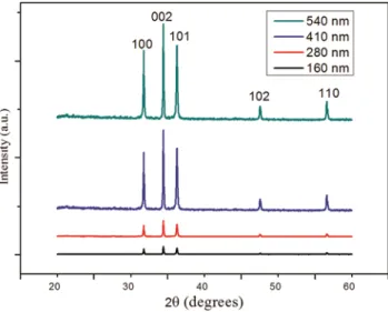
Figure 4 depicts the XRD graph for all the four samples. The XRD pattern is analysed from 20 to 60
Fig. 1 – (a) Prefabricated IDE and (b) thin film over IDE.
degrees as presented in Fig. 4. As can be seen from Fig. 4, all of the four samples indicates preferential
orientation along c-axis22. The peaks are identified to
(100), (002), (101), (102), and (110) plane of reflections for a single phase wurtzite ZnO structure. The diffraction peaks in the XRD spectrum are
matched with a pure hexagonal wurtzite structure23
(JCPDS No. 36-1451) for ZnO. The calculations performed using XRD graph is clearly indicating the increase in the crystallite size with the increase in thickness of the ZnO layer as shown in Table 1. According to this calculation the minimum grain size comes out to be 55.6 nm for the sample S1 and maximum grain size of 84.312 nm for the S4. It is clear from the results that there is an increase in the crystallite size with the increase in the thickness. Hence the sensitivity also increase as there is an increase in porosity but after a certain level the crystallite size becomes that much large that it starts
hindering the electron movements24. Hence the
sensitivity starts degrading after a certain thickness of the sensing layer of the sample.
3.3 Surface morphology
The FESEM micrographs have been shown in the Fig. 5. These SEM graphs depict the variations in the structures of all the four samples with their respective cross sectional views showing the thickness measurements for the four samples. The results may be elaborated for the increasing surface roughness of each sample in the increasing order of their thicknesses which suggests for the increased surface to volume ratio and hence the porosity. As reported in the previous studies the porosity and the surface to volume ratio plays an important role in enhancing the
gas sensing behaviour for a sensor25. The FESEM
micrographs shows the increasing porosity with increasing thickness and also it supports the results calculated using scherrer’s relation earlier which shows the increasing crystallite size with the increase in thickness of the sensing layer.
3.4 Gas sensing properties
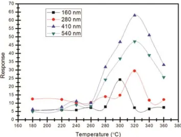
The gas sensing experiments for all the four samples have been performed with prior annealing at 200 °C for 1 h in a controlled environment so that, if any, gas particles are adsorbed over the surface of the sensor shall be desorbed before performing gas sensing. Figure 6 presents the sensing response of all the four samples wherein the sample S3 (410 nm) shows highest sensitivity of 63 towards the 500 ppm
of acetone vapours at an operating temperature4,26,27 of
320 °C. This shows that the optimum thickness for the sensing layer comes out to be 410 nm according to the present study. The samples S1, S2 and S4 also show high responses of 24.2 (at 300 °C), 29.5 (at 320 °C) and 47.2 (at 320 °C), respectively. Hence, it can be
Fig. 4 – XRD patterns.
Table 1 – Crystallite size calculations using Scherrer’s formula. Sample coding Peak position 2θ (°) FWHM B size (°) Dp (nm) Sensing response S1 34.4442 0.1563 55.606395 24.17 S2 34.4441 0.1498 58.014693 29.45 S3 34.4437 0.1093 79.479723 63.1 S4 34.4433 0.1031 84.312707 47.2
stated that the optimum sensing response for the sensor S3 is due to the perfect defect states created and the increased surface roughness which is directly linked to the surface to volume ratio. The results clearly show that the sensing responses firstly increase but after a certain thickness, it starts decreasing. This phenomenon may be explained using
the kinetics of molecules28-30. At low operating
temperatures, kinetics of the gas molecules will be lowered which decreases the rate of adsorption resulting in low sensing responses. Also, when the operating temperature rises above a certain limit, the kinetics of the gas molecules also increases in such a way that the molecules will escape before reacting with the active centres of the sensing layer again resulting in lowered desorption of gas molecules at
the surface of the sensing layer31. Hence, it results in
the decrease adsorption quantity of the gas molecules over the surface of the sensing layer. This will cause lowering down of the sensing responses of all the sensors below and above the optimum operating temperatures. Figure 7 (a,b) present the response and the recovery times for all the four samples at fixed concentration of 500 ppm acetone gas. It shows the variations in the response and recovery times for all the sensors at the temperature ranges from 180 °C to 360 °C. It is evident from the graphs that there is a continuous decrease in the response as well as the recovery times with few humps representing almost equal times for the adjacent operating temperatures. This decrease in both response as well as recovery times are again due to the kinetics of the gas
molecules at particular operating temperatures31.
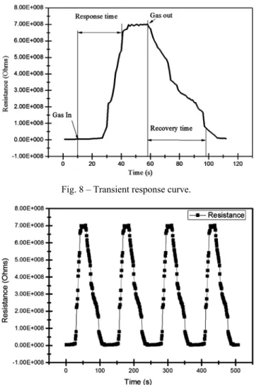
Figures 8 and 9 represent the transient response curve
Fig. 7 – (a) Response time and (b) recovery time.
and the stability and repeatability of the sensor S3 at
optimum operating temperature Topt = 320 °C towards
500 ppm acetone vapours in the air, respectively. The
sensor S3 shows a stable resistance in air (Ra) of 3.67
MΩ initially. Now, as the target gas acetone (500
ppm) is inserted in the chamber, its resistance (in gas
Rg) gradually increases to 2.32 GΩ in about 30 s
(response time). When the acetone gas is suctioned out from the GCTS, the sensor resistance starts decreasing and reached to its stable initial value in approximately 35 s (recovery time).
Figure 9 presents the reproducibility of the sensing results for at least six consecutive cycles (taken at an interval of 5 days each) without any degradation in the sensing response and the drift in the baseline. Further, the results clearly shows that the porosity and hence grain size with surface to volume ratio increases with the increase in thickness of ZnO sensing layer upto an extent (at particular annealing
Fig. 8 – Transient response curve.
Fig. 9 – Repeatability and stability of sensor.
temperature of 650 °C and thickness of 410 nm) beyond which the porosity of the film degrades causing the reduced oxygen vacancy sites over the sensing layer. This causes the degradation of sensing responses in the samples with thickness higher than 410 nm. Also as illustrated in Fig. 10, the adsorption and desorption phenomenon of the acetone gas over the ZnO sensing layers affected by the porosity of thin films.
According to previous studies26, these results can
also be explained using the activation energy concept, where the sensing mechanism of a sensor depends upon the chemical reactions over the surface of the sensing layer depends on activation energy. The higher activation energy results in the lowered electronic conduction in case of ZnO based acetone gas sensor. The previously reported literature, the ZnO thin film of thickness about 450 nm is having lowest activation energy as compared to other lower
and higher order thick films26.
Fig. 10 – Gas sensing mechanism. 4 Conclusions
ZnO thin films as sensing layers with varying thickness have been studied. Sol-gel spin coating technique is used for the fabrication of the sensing layers. The optical, surface morphological and structural properties has been studied and it was found that the porosity of the thin films increases with increase in the thickness of the sensing layer with increase in surface roughness and the grain sizes. Further, the sensor results conclude that the optimised thickness of 410 nm for a ZnO sensing layer at an operating temperature 320 °C shows a high response of 63.3.
Acknowledgement
Authors are thankful to Electronic Materials and Devices Laboratory, Department of Physics and Astrophysics, University of Delhi for granting permission to work in their laboratory.
References
1 Barsan N, Koziej D & Weimar U, Sens Actuators B: Chem, 121 (2007) 18.
2 Hsueh T J, Chang S J, Hsu C L, Lin Y R & Chen I C, Appl Phys Lett, 91 (2007) 053111.
3 Hsueh T J, Hsu C L, Chang S J & Chen I C, Sens Actuators B: Chem, 126 (2007) 473.
4 Lv Y, Guo L, Xu H & Chu X, Physica E: Low Dimens Syst Nanostruct, 36 (2007) 102.
5 Yang Z, Li L M, Wan Q, Liu Q H & Wang T H, Sens Actuators B: Chem, 135 (2008) 57.
6 Chen Y, Bagnall D & Yao T, Mater Sci Eng B, 75 (2000) 190. 7 Arora A, Arora A, George P, Dwivedi V & Gupta V, Sens
Transducers J, 117 (2010) 92.
8 Arora A, Arora A, Dwivedi V, George P, Sreenivas K & Gupta V, Sens Actuators A: Phys, 141 (2008) 256.
9 Saito S, Miyayama M, Koumoto K & Yanagida H, J Am Ceram Soc, 68 (1985) 40.
10 Bao D, Gu H & Kuang A, Thin Solid Films, 312 (1998) 37. 11 Sahay P, J Mater Sci, 40 (2005) 4383.
12 Christoulakis S, Suchea M, Katharakis M, Katsarakis N, Koudoumas E & Kiriakidis G, Rev Adv Mater Sci, 10 (2005) 331.
13 Zeng Y, Zhang T, Yuan M, Kang M, Lu G, Wang R, Fan H, He Y & Yang H, Sens Actuators B: Chem, 143 (2009) 93.
14 Wang G, Wang Y, Yau M, To C, Deng C & Ng D H, Mater Lett, 59 (2005) 3870.
15 Lee J B, Kim H J, Kim S G, Hwang C S, Hong S H, Shin Y H & Lee N H, Thin Solid Films, 435 (2003) 179.
16 Kolmakov A & Moskovits M, Ann Rev Mater Res, 34 (2004) 151. 17 Li L, Tong Z, Zhi-Jun W, Shou-Chun L, Yun-Xia T & Wei
L, Chin Phys Lett, 26 (2009) 090701.
18 Greiner A & Wendorff J H, Angew Chem Int Edn, 46 (2007) 5670.
19 Ueng T H, Tsai J N, Ju J M, Ueng Y F, Iwasaki M & Guengerich F P, Arch Toxicol, 65 (1991) 45.
20 Tyagi P, Sharma A, Tomar M & Gupta V, Sens Actuators B: Chem, 224 (2016) 282.
21 Dutta M, Mridha S & Basak D, Appl Surf Sci, 254 (2008) 2743.
22 Ilican S, Caglar Y & Caglar M, J Optoelectron Adv Mater, 10 (2008) 2578.
23 Raoufi D & Raoufi T, Appl Surf Sci, 255 (2009) 5812. 24 Katoch A, Abideen Z U, Kim J H & Kim S S, Metal Mater
Int, 22 (2016) 942.
25 Tyagi P, Sharma S, Tomar M, Singh F & Gupta V, Nucl Instr Meth Phys Res B, 379 (2016) 219.
26 Kakati N, Jee S H, Kim S H, Oh J Y & Yoon Y S, Thin Solid Films, 519 (2010) 494.
27 Qi Q, Zhang T, Liu L, Zheng X, Yu Q, Zeng Y & Yang H, Sens Actuators B: Chem, 134 (2008) 166.
28 Sharma A, Tomar M & Gupta V, Sens Actuators B: Chem, 176 (2013) 675.
29 Haridas D, Chowdhuri A, Sreenivas K & Gupta V, Sens Actuators B: Chem, 153(1) (2011) 89.
30 Bian H, Ma S, Sun A, Xu X, Yang G, Yan S, Gao J, Zhang Z & Zhu H, J Alloys Compd, 658 (2016) 629.
31 Kumar M, Kumar A & Abhyankar A, Ceram Int, 40 (2014) 8411.