Abstract— In order to transmit large amount of data over a
long distance, serial communications are used. If complex systems are running at different baud rates generated by some special baud rate devices, in this condition common serial ports were unable to meet the requirements. In this case without a unique baud rate controller one cannot implement multi-baud rate communication system. To solve this problem, in this paper we have designed a Multi-Channel UART controller which is based on FIFO techniques on FPGA. In M-C UART the data received at certain baud rate to the UART and that data can be transmitted to sub controller at the same or different baud rate. In designing of the digital circuits FPGA placed a major roles and it also improves the system integration, power consumption and reliability.
Index Terms—Multi-Channel UART (M-C UART),FIFO ,
FPGA, Baud Rate.
I. INTRODUCTION
In modern days due to the advancement in technology complex algorithms are easily implemented by modern micro-controllers and processors in order to achieve the expected system performance. In case of the control system the various factors are affected by the results of the system such as bit error rate, baud rate and also synchronization between the subsystems.
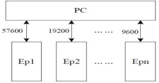
UART is one of the most used communication method in the computer system. Basically UART is a serial communication system and with the help of this system we can manage both parallel as well as serial data transfer, but in some of the communication system, serial or a parallel port are used to control the master and slave system. Parallel communication needs multiple bit address bus so it can be used for a minimum distance data transmission. In order to transmit large amount of data over a long distance, serial communications are used. When the complex systems are running on different baud rates with some special baud rate devices, the common serial ports are unable to meet the requirements. In figure 1, the equipment are set to different baud rates such as 57600 bps, 19200 bps, 9600 bps and some
other baud rates , while the PC baud rate is set to 115200 bps, in this case without a unique baud rate controller we cannot implement multi-baud rate communication system[3].
Figure 1: Multiple equipments communication
6 DOF robot consist of 6 sub controller which are of similar structure. The sub controllers are controlled by the control parameters that are sent from the PC. RS 485 bus net is used for communication between the PC and sub controllers. The PC will identify the sub controllers based on the distinctive address number. When the PC wants to send data to node 6, it has to access front 5 nodes, which reduces the algorithm precision and engenders the time delay. This brings down the performance of the robot[3].
Figure 2: 6 DOF robot
Design of M-C UART controller based on
FIFO technique on FPGA
A. Problem Statement
UART three disadvantages, which influence its efficiency, are listed below
In an ordinary UART it has only single channel. Used to connect a single device so when the number of the chip increases on the devices which may cost a lot of space and resource?
In a flame operation of the microprocessor interrupt request are used to notify the operation. When many interrupt request occurs the processor stuck so the processor efficiency will reduces because number of interrupt request and a few characters are transmitted during each time
In processor the data bus is 32 bit but some of the cases only one byte of the transmitted by the controller to the processor at a time so more number are not used properly.
The above 3 stated problems are solved by using more UART channels in a single chip. So in this proposed paper we are implementing parallel processing data, interrupt control mechanism with the help of MULTI-CHANNEL UART controller based FIFO technique and realization is implemented using Verilog HDL on FPGA.
II. RELATEDWORK A. Synchronous Serial Transmission
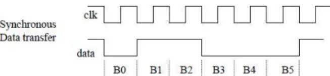
In Synchronous Serial transmission both the sender and receiver must share a clock with each another, or strobe provided by the sender or other timing signal so that the receiver knows the next bit of the data which is read. There is no data available for most of the serial synchronous communication for instant to transmit so that fill character must be sent. In Synchronous communication only one data bits are transmitted between the sender and the receiver so it is efficient, in a printers and fixed disk devices uses the synchronous transmission and it uses one set of the wires for data transmission in single clock source., the printers and disk devices they not normally serial devices because it interface the standards to send an entire word of data in a clock pulse and PC does not support the standard communication hardware.
Figure 3: Synchronous Data Transfer
B. Asynchronous Serial Transmission
In Asynchronous serial communication it uses the protocol to communicate between the sender and the receiver, it uses the 2 signals such as start signal to start communication with each and stop signal to stop communication with each other. Start signal it tells the receiver to prepare the receiving mechanism and symbol of registration, stop signal is to bring the receiver mechanism to rest in preparation for the reception for the next data, ASCII codes used as a start and stop bit.
Figure 4: Asynchronous Data Transfer
C. The UART
The UART is basically a computer hardware device used to transmit the data in between parallel as well as serial form and UART it uses TIA and RS-232 AND 485 communication standard. In UART the format of the data and speed can be configurable so the name is called universal and also driver circuit it handles the electric signaling and methods. UART is a part of ICs used in computer systems for serial communications.
UART are basically implemented in microcontroller units and it also supports dual UART in a single chip and also octal UART supports eight UART in a single chip. In a UART the bytes data is transmitted individually in a sequential fashion at the second UART recombines the bits of data as a byte in a UART shift register act as a conversion of serial and parallel form. In UART serial module it is divided into sub module such as transmitter module, receiver module and baud rate generator.
D. Asynchronous FIFO
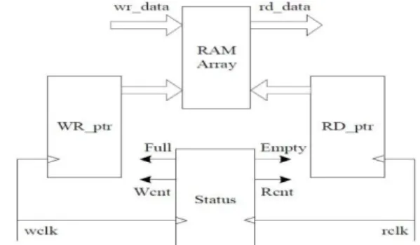
When a FIFO design the data values are written at the FIFO buffer from one clock and data value are taken from the same FIFO buffer with different clock and two clock domains used are asynchronous. FIFO are used at data cache and storing difference of frequency and this is also used to safely and quickly pass the data from one clock to another clock domain. Periods and phase of the clock are completely independent in the asynchronous clock circuit so that the data
FIFO based FPGA which includes high reliability and high write and read speed. FIFO it consisting of a status block, write and read pointer, RAM array. To store a data separate read and write ports are used. Writer pointer are used to point the next written and read pointer are used to read the next. Writer pointer are incremented by a write operation and read pointer increments the read operation, if resets the both the pointers it indicates the FIFO is zero. Invalid data is pointing by the reader pointer and the next FOFO location is written by the writer pointer. The status block is used to generate full and empty signals of the FIFO. Full signal it indicates FIFO cannot accommodate larger data and empty signal it indicates FIFO cannot readout more data. Wclk signal is used to writing the data into FIFO and Rclk is used to reading the data from FIFO[8]
Figure 5: Asynchronous FIFO structure diagram
E. Solutions for Metastability
Unpredictable problems in a FIFO are caused by metastability, so reduce the metastability at the time of designing. The system is a synchronous element, metastability is avoidable. It is difficult to eliminate the metastability completely so that we need calculate the probability of error in terms of time MTBF is used measure failure probability. The time signal changes instantaneously from zero to one at a D Filp-Flop and the value of the Q is uncertain it is called as metastability FIFO needs synchronous to counter clock and sample value if the counter clock, in this condition counter changing from FFFFF to 00000 it indicates every single bit goes metastable, in order to overcome the probability if concurrence we should make one bit change every time in the counter increments so we use the gray code counter[5].
The gray code and binary code is as follows.
Figure 6: Architecture of Gray code counter
F. Multi-Channel UART
In Multi-Channel UART (M-C UART) is having multiple transmitters and receivers and channels, which are working independently or together. The data can be transmitted/received over the channel by different or same baud rate. To reduce the CPU overhead, M-C UART are used. At any time CPU can read the complete status of the channel and with the help of the start and stop bit synchronization for the serial data stream is accomplished. To enhance the data integrity one, more parity bit can be attached. To check the transmission bit error the receiver uses the parity bit. Different baud rate are used by the channel to receive and transmit the FIFO and cpu register. In order to modify the parameter users can go with top level of the source file. In M-C UART for transmission of the data to the system the channels m UARTs are used which perform independently and it uses the same logic to reduce the size, cost, and customization.
III. IMPLEMENTATIONOFM-CUART
Figure 7: Block diagram of Multi-Channel UART
The M-C UART contains the main block out of nine blocks, 4 blocks are UART and 2 blocks are Asynchronous FIFO, controller block, register block, baud rate generator block.
A. Hardware structure design of UART
As shown in the above figure 3. UART circuit block is having 3 parts they are: transmit circuit, receive circuit and control/ status register. Transmit circuit having transmit buffer and shift register, transmit buffer is used to load data being transmitted and data is accepted from the shift from the transmit buffer and send it to TXD pin. The receiver circuit is having the receiver buffer and receiver shift register. The data received by the receiver shift register from RXD. The receiver buffer is used to load the data. Control register is a special function register used in UART to control. UART choose the different communication method according to the bits and it knows what to be received or what to be transmit. Data is received from external device used by the FIFO. In different clock frequencies FIFO writing the data and reading the data according to the system baud rate so we have to communicate with different baud rates and controller is used generate the different baud rate for communication.
Figure 8: UART block structure
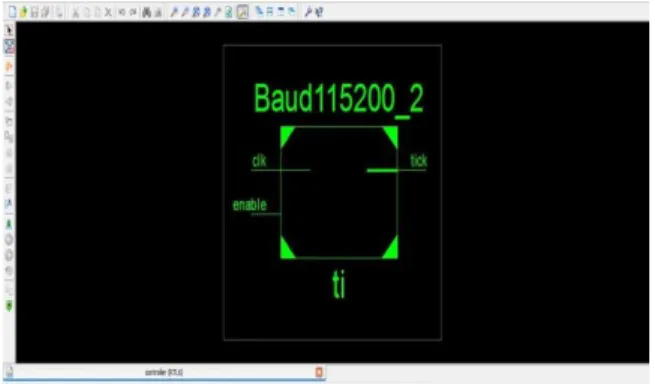
B. Multi Baud Rate Generator
In UART transmission different baud rate are generated by the baud rate generator. The communications it including buses and controller interrupts, reading and writing signals is managed by the CPU between the processor and controller. Interrupt request are controlled by the interrupt controller. In order to improve the system efficiency is to accomplish more number of tasks in less time. There are mainly two methods are using to design the implementing task in parallel as many as possible to reduce the implementation time.
Figure 9: RTL schematic of Baud Generator
C. UART Transmitter
The stored data is sending by FIFO from the microprocessor and data is still in under transmission on the TXD line. The start bit and stop bit attached by the parity checkers to check the filling frame. Two serial operations are done in the process of frame this are system choke points , first one is sending serially and receiving notification while writing into amends at the time of frame delivered and choke point will be eliminated.
Figure 9: State Machine of Transmitter Module
As shown in the figure 9. data is sending serially with help of finite state machine. This machine works with the help of start bit and stop bit which are driven by baud rate clock. The last count of the stop counter, the machine switches to notify state from stop state. Notify state it defines generated of notifications at the last stop bit. The state machine goes to either state because of main clock. The frames send serially by the shift register through TXD lines and it creates the signal TXD by serial data transmits.
Figure 10: UART TXD
The RTL Schematic of the Transmitter module is as shown below
Figure 11: RTL schematic of Transmitter module
D. UART Receiver
RXD lines are used to receive the data in a UART receiver.
The parity checkers are corrects the frame is received and also checks the received frame to know whether the receiving frame is wrong. The difference between the receiving and sending flow the transmission velocity of the data is faster than receiving velocity. The state machine of the baud rate clock with sample input signals as shown in the figure 12. In this module check state indicates the data state, stop and take responsibility of the parity check. The design is based on the baud rate and clock is 16 times faster than input signal so that enough clocks provides to check parity at time arrival of the stop bits and parity checkout can be implemented in signal sampling process.
Figure 12: State machine of receiver module
The state machine will notify the last counts of the stop bit for FIFO to store the received data. The design flow indicates that all the data is stored in FIFO correctly and system efficiency is improved in this way.
Figure 13: UART RXD
The RTL schematic of the Receiver Module is as shown below
Figure 14: RTL schematic of Receiver module
E. Transmitter FIFO
The processor clock is faster than the baud rate clock so that the microprocessor data is usually arrives at the moment when there are data under transmission. The system is waiting from the transmission this is second choke point, during the transmission the fresh data also buffered. The FIFO width is 8 bit and adapted in this design called as width of the data bus. RAM integrated in FPGA used to realize the design of the FIFO to reduce the usage of the FPGA. The input bit width and output of the FIFO should be same and shift register length same as the frame length is shorter than 8 bit so logical elements (LEs) required, so it will be used as buffer between the FIFO and shift register.
F. Receiver FIFO
In receiver FIFO sending FIFO which is used to prevent the data and it focuses reducing the interrupt frequency. When the quantity of the data stored in FIFO the receiving interrupt are generated. The value between the zero and the FIFO depth is called as threshold value. The 8 bit register and the data length indicator operate in the same manner in a receiving sequence. 32 bit bus can be utilized to increase the transmission velocity. The data length needs to be access the over time interrupt to reduce the reading time of the processor.
G. UART Block diagram
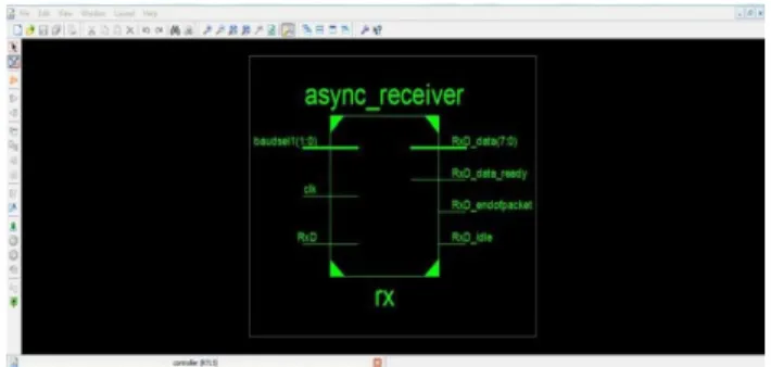
As we can see that from former traditional UART we have designed and developed the UART with two Asynchronous FIFO attached to the transmitter and receiver modules of the UART using the Verilog HDL language. This single module is four times module instantiated by to obtain a M-C UART functionality. The M-C UART can be run in different programmable modes. The controller enters the IDLE state if CS is low, during the idle state all the UARTs are disabled, when the controller enters the RUN state, during the RUN state the M-C UART controller operates.
Figure 15: Single UART block controller
Figure 16: RTL schematic of single UART controller
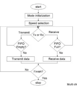
H. Software design Structure
In this paper I have used Verilog HDL codes to design FPGAs hardware architecture, the implementation of the codes in this software is very easy .The software design flow is as shown in figure 17.
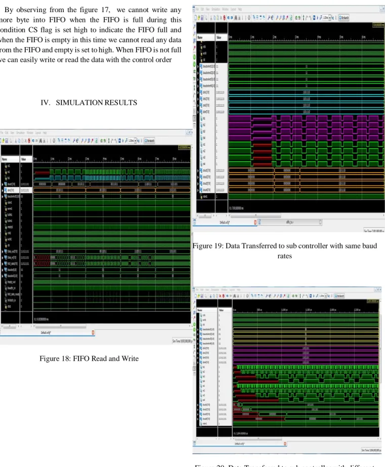
By observing from the figure 17, we cannot write any more byte into FIFO when the FIFO is full during this condition CS flag is set high to indicate the FIFO full and when the FIFO is empty in this time we cannot read any data from the FIFO and empty is set to high. When FIFO is not full we can easily write or read the data with the control order
IV. SIMULATIONRESULTS
Figure 18: FIFO Read and Write
Figure 19: Data Transferred to sub controller with same baud rates
Figure 20: Data Transferred to sub controller with different baud rates
V. CONCLUSION
In this paper i have implemented Multi-Channel UART controller based on asynchronous FIFO within the FPGA. The design of asynchronous FIFO technique based SRAM with has high reliability and high speed. This M-C UART controller can be implemented in complex modern communication system where the system works at different baud rates. In the complex control system the time delay can be reduced between the sub-controller and synchronization can be achieved with the sub controllers. Since I have designed the controller on FPGA, we can easily is reconfigurable and scalable.
REFERENCES
[1] C. E. Cummings, “Simulation and Synthesis Techniques for Asynchronous FIFO Design”, SNUG San Jose 2002. [2] "Avenet Core", datasheet Multi-Channel UART Version 1.0 July 2006.
[3] "Implementation of a Multi-channel UART controller based on FIFO technique and [4] FPGA", IEEE Conference on Industrial Electronics and Applications 2007, ICIEA. 2007.
[5] "Understanding Metastability in FPGA", Altera.com Ver.1.2, July 2009. [6] http://www.design-reuse.com/sip/6-5990/multi-channel-uart [7] http://www.altera.com/leterature/wp/wp-01082-metastabilit y.pdf
[8] Vijay A. Nebhrajan, “Asynchronous FIFO Architectures”, www.eebyte.com
Safinaz S1 , Assistant Professor , Department on
Electronics and Communication Engineering, Sir M Visvesvaraya Institute of Technology, Bengaluru, Karnataka, India.
Kiran N V2, is cuurently pursuing his M.Tech Electronics
Engineering at Sir M Visvesvaraya Institute of Technology, Bengaluru, Karnataka, India.