IMPLEMENTATION AND DESIGN OF 6T-SRAM WITH READ AND
WRITE ASSIST CIRCUITS
M. Adiseshaiah* D. Sharath Babu Rao** V. Venkateswara Reddy***
ABSTRACT
In today’s world high performance workstations and servers demands fast memory access times to keep up with heavy work load imposed upon them. If we assume that one of the goals of main memory technology is to produce a high bit density component, a part that requires six transistors per cell may not be the best choice. Many of the researchers and companies have been tackling the various problems that accompany the scaling. However, the transistor miniaturization also introduces many new challenges in very large-scale integrated (VLSI)
circuit design. In the sub-100-nm CMOS generation, a large local Vth variability degrades
the 6T-SRAM cell stability, so that we have to consider this local variability as well as the global variability to achieve high-yield SRAM products. Therefore, we need to employ some assist circuits to expand the SRAM. The SRAM with 120nm technology technique the power is 13.243mW and the SRAM with 65nm technology technique is 3.821mW. The total power saving is 71.14%
*Assistant Professor, Department of ECE, Ananthalakshmi Institute of Technology, Ananthapur, A.P
**Lecturer, Department of ECE, JNTU College of Engineering and Technology, Anantapur (DT), A.P
1. INTRODUCTION
Fast memory access times are essential to cater the heavy workload needs imposed on PCs and work stations. With many users of PCs and work stations connected to local area network (LAN) and wide area networks (WAN), the need for fast memory access is essential DRAM operating fast page made offer some relief for the “access time blues” CMOS Technology has progressed rapidly with regard to Moore’s Law. Many researchers and companies all over the world have been tackling the various problems that accompany the scaling. Now a day the aggressive scaling of the transistor size drastically affects SRAM devices, which are widely used in many digital chips such as cache and so on. This is because the SRAM cell generally employs the smallest transistor size in each technology generation to achieve a smaller chip size. Figure1 shows that the trend of six-transistor 6T-SRAM cell size from 180-nm technology downward.
Figure 1 Technology versus SRAM Cell Size
The SRAM cell size shrinks by about 50% as one generation of technology advances. In 65-nm technology, SRAM cell sizes of about 0.5 µm2 have already been reported. In the 6565-nm CMOS generation, a large local Vth variability degrades the 6T-SRAM cell stability. The Vth
variability is divided into local and global components. The local Vth variability occurs due to
fluctuations of the doped impurities, while the global Vth variability occurs mainly due to the
manufacturing process. Vth variability occurs mainly due to the manufacturing process, which
leads to variations in the MOS transistor’s physical dimensions such as gate length (L), gate width (W) and gate oxide thickness. As the transistor size shrinks with the advance of technology, because the accuracy of the physical dimensions is improved due to the advance of manufacturing equipment, then the global Vth variability is mostly maintained.
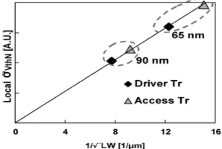
Figure 2 Plot of SRAM nMOS transistors of 90-nm and 65-nm technologies
Fig.2 shows the sigma of the local Vth variability of SRAM nMOS transistors using 90-nm
and 65-nm technologies the local Vth variability is in proportion to the inverse square root of
the transistor channel area LW. If the transistor size shrinks in accordance with the advance of technology, the sigma of the local Vth variability increases. This indicates that scaling degrades the local Vth variability. In 65-nm technology, it is difficult to keep a sufficient
operating margin using only the write assist circuitry and it is essential to use both read and write assist circuitry.
II. IMPLEMENTATION OF SRAM
This chapter gives the detailed implementation of SRAM, the circuitry involved in designing the SRAM and the operation of each block in the design.
A. Architecture
The block diagram of the SRAM chip is shown in Figure3. The core memory (32 bit) is arranged in an 8x4 array of 6-transistor (6T) SRAM memory cells. The square layout is efficient in terms of silicon area. It also provides a balanced bit line and word line capacitance for optimal access time.
B. Sense amplifier
Figure4 shows the circuit schematic of the bit line sense amplifier. A cross-coupled inverter latch is popular in low power designs due to negligible static power consumption. Typically, this type of sense amplifier detects a voltage difference of one tenth of the VDD. However, the
power consumption is still higher for this kind of sense amplifier because it requires that the current source turn on slightly before the voltage swing is applied. Therefore, the current source is on for this extra delay and consumes static current [1], [5].
Figure 4 Schematic of the Bit Line Sense Amplifier Circuit.
Normally the Pre and SAE signals are low. Hence the bit lines are pre charged to VDD and the
internal nodes of the sense amplifier follow the bit line voltage (VDD) but the sense amplifier
does not operate (no path to ground). During a read operation, the Pre signal is pulled high and one of the bit lines discharges. After a small time delay when the BL discharges to a voltage low enough to be detected by the sense amplifier (typically one tenth of the VDD),
SAE signal is pulled high. This activates the sense amplifier and disconnects the internal nodes of the sense amplifier from the bit lines. Now the internal nodes of the sense amplifier reach the rail-to-rail swing and the data is latched by a delayed version of the SAE signal (Sel_latch signal) as explained in section C.
C.Multiplexer, latch and output driver cell
enable (SAE) signal. Similar to the DMUX, in this case the 16-bit output data word is selected by the column decoder outputs [1], [5].
Figure 5 Circuit Schematic of the MUX, Latch and Output Driver Cell
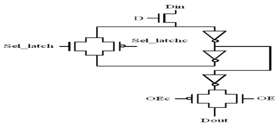
D. Demultiplexer, latch and input data driver cell
Figure 6 shows the circuit schematic of the demultiplexer (DMUX), latch and input data driver cell. The demultiplexer is implemented in pass-transistor logic due to low-transistor count and fast operation. Since the input data can be '0' or '1', a transmission gate is used instead of a NMOS pass transistor. The transmission gate is controlled by the column-decoder outputs.
The column decoder generates both the select signals and their complements. The latch is used to retain the data when the cell is not selected (D0 = '0'). The latch is implemented using two cross-coupled inverters and a transmission gate. The data is stored due to positive feedback action similar to the conventional SRAM cell. When the data is written in the memory (WE = '1'), the transmission gate disconnects the cross-coupling mechanism of the latch. At this moment the input data (Din) is transparent to the BL provided the select signal is present (D0 = '1').
Figure 6 Circuit Schematic of the DMUX, Latch and Input Driver Cell
In the Figure 6 BLc is the complement of Bit line, D is the input to the D Latch and Dc is the complement to it, WEc is the complement of Write Enable. As soon as the WE signal goes away, the transmission gate conducts and the data is latched by the positive feedback mechanism. Instead of transmission gates, simple NMOS pass transistors can also be used to achieve the same operation. However, an NMOS does not transfer a logical high faithfully. It inserts a voltage drop of Vt, the threshold voltage of the transistor under the body effect (source terminal is at a higher voltage than the substrate). This reduced swing goes to the input of the inverter and causes a static current from VDD to ground. Therefore, for the low
power design, we have used the transmission gates. Since the bit lines are highly capacitive, large inverters are added along with the transmission gates to drive the BLs [1], [5].
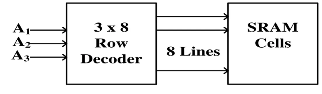
E. 3x8 Row Decoder
The row selection circuit decodes the row address and activates one single row. This row is shared by all word line signals of the row. The row selection circuit is based on a multiplexer circuit. One line is asserted while all the other lines are at zero. In the row selection circuit for the 8x4 array, we simply need to decode a two- bit address. The block diagram of the 3×8 row decoder and its associated circuitry is as shown in Figure 7. The decoder selects one of 8 lines, as per the address lines. The output of the decoder is fed to the rows of SRAM cells. The row decoder selects one of those rows, depending on the seven-bit address given to it. The entire system is explained in details later.
3 x 8
Row
Decoder
SRAM
Cells
A
1A
2A
38 Lines
Figure 7 Block Diagram of 3 x 8 Decoder
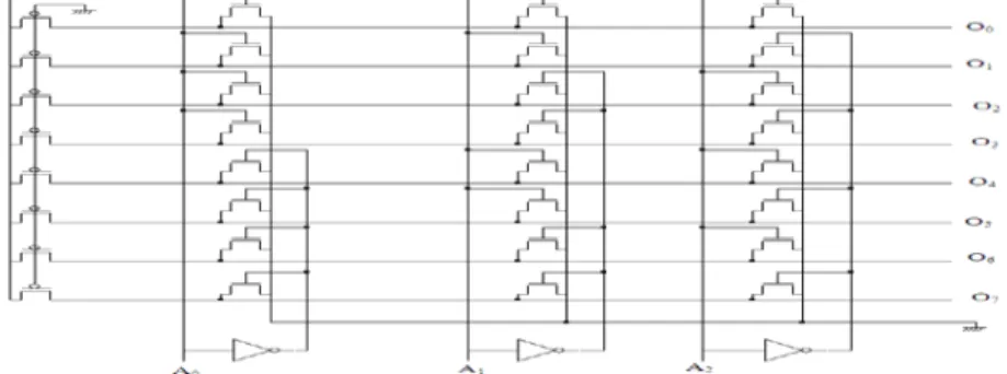
have used a dynamic NOR decoder. This structure reduces the number of transistors by half. It also increases the speed of the decoder and makes the layout simple and less time-consuming. The structure of 3 to 8 row decoder is shown in Figure 9. In the Figure 8 A0, A1,
A2are the inputs to the decoder and O0 …O7 are the output lines [1], [5].
Figure 8 Schematic of 3 x 8 NOR row decoder
F. Working Of NOR Decoder
The NOR decoder works like any other dynamic circuit. It requires a pre-charge cycle followed by the evaluation stage. These stages are as explained below. The ‘Pre-charge’ input is asserted which turns ON the PMOS devices and all the outputs of the decoder go to VDD
(Logic ‘1’). The decoder should not be read at this instant, since all the outputs will be at VDD. Evaluation Stage: Once the pre-charge is done, the PMOS device is turned OFF. The
outputs will still be at Logic ‘1’, because the charge will be stored on the capacitors. Now the inputs are applied on the three address lines. The corresponding NMOS devices will be turned ON and the charged capacitor on that line will be discharged to ground. Thus, all, except one line will go to ground (Logic ‘0’). The line, which remains high, will be the decoded line and this line will drive all the NMOS transistors on that line. Thus, the right data will be available on the data line. This data will be given to the output data block, which will return the correct data to the outside world when the Out Enable signal is asserted. The selected line will have to drive a number of transistors and so we will need a series of buffers to drive such a heavy load. The number of buffer stages required to drive the transistors, without compromising on the speed [1], [5].
G. 3x8-Column Decoder
The column address decoder shown in Figure 9 is similar to the row address decoder with the addition of a pass transistor. The pass transistor is connected to the bit lines. The tree decoder portion of the column decoder is sometimes called a pre decode. An enable can be used here as well. In the Figure 9 A0, A1, A2 are the inputs to the decoder and O0 …O7 are the output
Figure 9 the schematic of a 3x8-column decoder
The column decoder circuitry is designed to select one out of 2M columns of the RAM array according to an M-bit column address, and to route the data content of the selected bit line to the data output. The tree based column decoder consisting of consecutive stages is shown in Figure 9. In this case, the pass transistor network is used to select one out of every two-bit line at each stage, whereas the column address bits drive the gates of the nMOS pass transistors.
The advantage of tree-based decoder is that much reduced transistor count. The disadvantage is that large number of series connected nMOS passes transistors [1], [5].
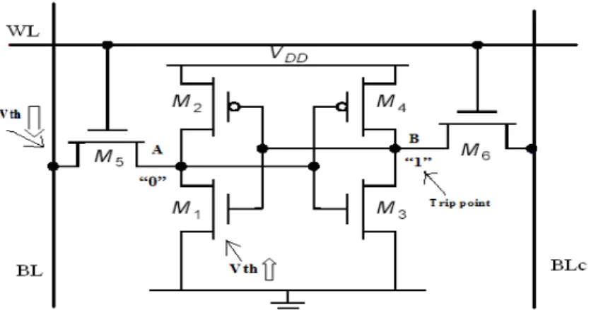
I.SRAM cell with when read fails.
When the WL turns on node A will rise due to voltage divider action between M5 and M1. If this level is higher than the trip point on of the INV (M3, M4) the latch will loose its state then its read fails.
J. Read and Write assist circuit technique in 65nm
Figure 12 Circuit Schematic of 6-T SRAM Cell with read & write assist circuit
In order to achieve a higher yield for SRAMs using the straight cell, we propose a read assist circuit. Figure shows this circuit. The read assist circuit improves the SNM by slightly lowering the word line (WL) level rather than the SRAM memory cell power supply [4]. The WL level is held below the memory VDD. Read current is reduced, and write is more difficult.VDD level of the bit cell above the WL voltage. This will increase the gate drive of the Pull-Down device and improve SNM. During a read, VDD of all columns must be raised. When the memory is inactive, the lower VDD will reduce leakage [6].
III. Circuit Implémentation
A. 6T SRAM Cell
Figure 13 shows the schematic of a 6T SRAM Cell, In the Figure 14 the layout of this cell is shown and followed by its output in Figure 15.
The 6T SRAM cell shown in the above figure has two outputs BL and BLc and one input WL. BL is real value and BLc is the complementary value.
Figure 14 Layout of 6T SRAM cell in 120µm technology
The layout is having six transistors and two metal lines lead the outputs. The ‘data’ and ‘~data’ signals similar to ‘BL’ and ‘~BL’ in the schematic, ‘Word line’ are the ‘WL’ signal.
Figure 15 Output of 6T SRAM Cell Layout in 120µm technology
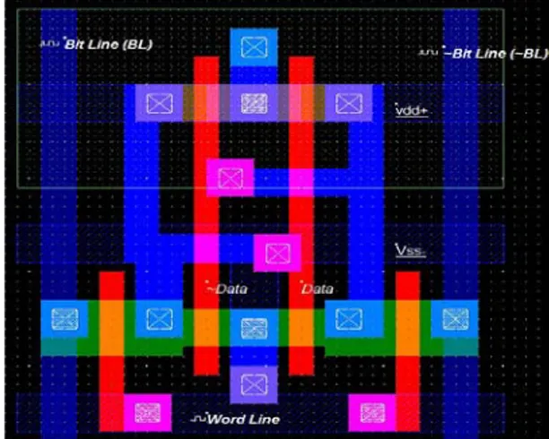
B. 6T SRAM Cell with read and write assist circuit
Figure 16 Layout of 6T SRAM cell in 65nm technology
In the above layout, the inputs and outputs are same as that of the general 6T SRAM cell, extra inputs “bit line”, “~ bit line” is the gate input signal to the SRAM, and “clk” is the extra inputs for the read and write assist circuit.
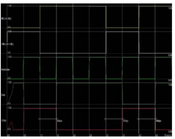
Figure 17 Output of 6T SRAM Cell Layout in 65µm technology
IV. RESULTS
Figure 18 Layout design of 32-bit SRAM in 120nm
The layout for 32 bit SRAM is shown in Figure 18 and the simulation results of the layout is shown in Figure 19. In this section, the design of SRAM designed with 120nm technology using Micro wind Version 3.0 is shown. The waveforms thus shown in Figure 19 give a clear view of the address bits and the data bits. The layout obtained is the combination of all the individual blocks discussed in Chapter III. All the basic modules are integrated to form a 32-bit SRAM. The layout, decoders with less number of transistors are chosen to optimize the area.
Figure 19 output of 32-bit SRAM in 120nm technology
B. Layout for a 32 bit SRAM in 65nm technology
The layout for 32 bit SRAM in 65nm technology is shown in Figure 20 and the simulation results of the layout is shown in Figure 21
Figure 20 Layout design of 32-bit SRAM in 65nm
The Figure 20 is the layout of 32-bit SRAM designed by incorporating the read and write assist circuit in 65nm technology logic to the general SRAM circuit shown in the Figure 18.
Figure 21 Output of 32-bit SRAM in 65nm technology
B. Comparison of powers dissipation of SRAM in 120nm & SRAM 65nm
technology
Now the power dissipation, which was monitored on the output window of the practically implemented for both the SRAM’s, one in 120nm and other is with 65nm technology shown below.
The power dissipation have been monitored for both the SRAM’s, the monitored part of the power dissipation is shown in Figure 22.
V. CONCLUSIONS
The 65nm technologies SRAM is implemented with read and write assist circuit technique. The project has been very challenging since it includes functional validation, transistor sizing, and layout of various circuits. Full functionalities of all the design features have been validated. Based on simulation results for the circuit it can be concluded that read and write assist circuitry is effective controlling power dissipation. Finally, the power dissipation of both the circuits incorporated is compared. The future scope of this project is density of the SRAM circuit can be increased by using less transistor SRAM cells. The performance of the module can be improved using low voltages. A 128 x 128 SRAM can be implemented using the basic module of this project. Speed of the SRAM can be improved by scaling down the technology.
VI. REFERENCES
[1] J. M. Rabaey, A. Chandrakasan, B. Nikolic, “Digital Integrated Circuits, a Design Perspective” Prentice-Hall India, second edition, 2003.
[2] David.A.Hodges, Horace G Jackson, Resve A Saleh, “Analysis and Design of Digital Integrated Circuits” Tata Mc Grawhill. Third edition 2004.
[3] M. Kanda, K.Takahashi, H. Oyamatsu, N. Nagashima, and M. Kakumu, “Highly stable 65 nm node (CMOS5) 0.56 _m SRAM cell design for very low operation voltage,” in Symp. VLSI Technology 2003Dig. Tech. Papers, Jun. 2003.
dynamic power supply,” IEEE J. Solid-State Circuits, vol. 41, no. 1, pp. 146–151, Jan. 2006
[5] A. P. Chandrakasan el al., “Low-power CMOS digital design,” IEEE Journal of Solid-state Circuits, Vol. 27, pp. 473-484, Apr. 1992.