Identifying Model Parameters
of Semiconductor Devices
Using Optimization Techniques
Josef Dobe
s
ˇ
1, Martin Gr´abner
1and Lubom´
ı
r Hru
ˇ
skovi
c
ˇ
21Department of Radioelectronics, Czech Technical University in Prague, Czech Republic 2Department of Electromagnetic Field, Czech Technical University in Prague, Czech Republic
The optimization is an indispensable tool for extracting the parameters of any complicated models. Hence, advanced optimization techniques are also necessary for identifying the model parameters of semiconductor devices because their current models are very sophis-ticated(especially the BJT and MOSFET ones). The equations of such models contain typically one hundred parameters. Therefore, the measurement and particularly identification of the full set of the model parameters is very difficult. In the paper, an optimization method is presented which is applicable for the identifications of very complicated models using a relatively small number of iterations. The algorithm has been implemented into the original software tool C.I.A.(Circuit Interactive Analyzer) to its static and dynamic analysis modes. Therefore, the optimization is able to identify both direct-current and capacitance models of semiconductor devices. The process is demonstrated with various transistors.
Keywords: modeling, semiconductor device,
measure-ment, parameter extraction, optimization, BJT, MOSFET, JFET
1. Introduction
For identifying the model parameters, both spe-cial and generally usable tools are used. The special tools usually work in multistep mode
(i.e., the parameters or their groups are extracted successively), and therefore they are more ro-bust than the generally usable ones. The extrac-tion procedure for the EKV 2.6 MOSFET model
[1] is the typical representative of this group. On the other hand, the MATLAB Optimization Toolbox[2]is one of the main representatives of the generally usable tools(this implementation contains several powerful optimization meth-ods – e.g., preconditioned conjugate gradient,
Levenberg-Marquardt, or Gauss-Newton). The procedures of such tools usually determine the model parameters en bloc, and therefore they are not so reliable as the special tools. More-over, they often need large number of iterations. However, they are able to optimize more com-plicated structures.
The C.I.A. optimization procedure belongs to the generally usable ones – the algorithm seeks to find up to 25 (in the current stable version of the program)unknown parameters of the cir-cuit for the fulfillment of user-specified require-ments. The algorithm controls the analyses and changes these parameters after each of them to successively fulfill the user’s requirements.
2. Description of the Optimization Procedure of the C.I.A. Program
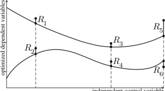
Let us assume that two circuit output variables are to be monitored at three points as shown in
independent control variable
optimized dependent variables
R1
R2 R3
R4
R5
R6
Figure 1. The circles mark the user-specified requirements on the output variables, and the squares mark values of the output variables ob-tained after an analysis. The algorithm seeks to minimize the sum of squares of differences between them
S(x1, . . . ,xn) = m
k=1
R2k(x1, . . . ,xn), nm,
(1)
where the optimized parameters of the circuit are marked byx1, . . . ,xn, andRk, k=1, . . . ,m
are the differences.
An extreme(local or global)of the function of
nvariables(1)is found in the standard way, i.e., solving system
∇S=
m
k=1
2Rk∇Rk =0. (2)
After the standard derivation(e.g., see[3]), the generalized least-squares procedure is obtained applying the condition(2) (tmarks matrix trans-posing)
JtJΔx(l) =−Jtr, x(l+1) =x(l)+Δx(l),
l=1, . . . ,lmax, (3)
wherelis the iteration index and
rk=Rk[x(l)], ∂∂rxk i =
∂Rk
∂xi[x
(l)],
J=
⎡ ⎢ ⎢ ⎢ ⎢ ⎣
∂r1
∂x1 · · ·
∂r1
∂xn
... ...
∂rm
∂x1 · · ·
∂rm
∂xn
⎤ ⎥ ⎥ ⎥ ⎥ ⎦,
k=1, . . .m, i=1, . . . ,n.
(4)
The generalized least-squares procedure is very fast, but sometimes insufficiently robust. There-fore, the method is combined with the classical gradient one
Δx(l) =−2Jtr, l=1, . . . ,lmax
to the more reliable(Levenberg-Marquardt) mod-ification of(3)
[JtJ+λ(l)1]Δx(l) =−Jtr,
x(l+1) =x(l)+Δx(l), l=1, . . . ,lmax, (5)
where 1 is unit matrix and λ(l) is a scalar
iteration-dependent factor. There are many methodologies to optimally determine that fac-tor at each iteration – the most sophisticated ones use an estimation based on the eigenval-ues of the Jacobian (4) [4]. However, simpler empirical ways are mostly also successful[2,3]. The procedure of the C.I.A. program also con-tains an original version of the empirical method
(however, the method based on the eigenvalues of JtJ is also developed), which tries to de-crease theλ(l)factor successively(i.e., to make
the generalized least-squares method more in-fluential at the end of the process):
λ(1) =1,
λ(l+1) = λ(l)
5 .
(6)
However, this monotone decrease must be inter-rupted(and therefore the gradient method must be sometimes made more influential)when the method seems to diverge:
if l>1 ∧ S(l) min
j=1,...,l−1S
(j) then
x(l) :=x(l−1), λ(l) :=λ(l)52, (7)
where the first multiplication by 5 compensates the division by 5 in(6), and the second multi-plication by 5 increases the scalar factor of the method.
Let us emphasize that the procedure (5)–(7)
does not use usual one-dimensional minimiza-tions. This is why the method of the empirical determination of the scalar factor is quite dif-ferent from that in MATLAB [2]. However, the suggested procedure is appreciably faster – it needs tens or hundreds of iterations com-pared with thousands typically necessary for the same tasks in MATLAB(we tested three built-in methods).
• the differencesRk in (4)must be
normal-ized;
• the differences should also be weighted so that a measurement inaccuracy can be con-sidered;
• the JacobianJin(4)mustalsobe normal-ized;
• the Jacobian should be determined quickly, using the sensitivity analysis;
• evaluating the Jacobian is not necessary in each iteration – the criterion has also been developed;
• a logarithmic damping suppressing possi-ble divergence of iterations (5) has also been included.
2.1. Normalizing the System Equations
The models of semiconductor devices contain expressions with extreme differences of their magnitudes(tiny terms together with huge ones). For such systems, many of the standard opti-mization algorithms[3] are numerically unsta-ble. Hence, a normalization of(5)is necessary. First, the differences are normalized together with their weighting:
Rk[x(l)]wk
y(kident) x(l)−y(kmeas)
|y(kmeas)|+y(knull) , k=1, . . . ,m,
(8)
where(meas) and(ident) mark the measured and
identified values, and the parametersy(knull) sta-bilize(8)when some measured values are near or equal to zero. However, many numerical ex-periments have proven that a normalization of the Jacobian is also necessary:
∂Rk x(l)
∂xi :=wk
∂y(kident) x(l)
∂xi
× x
(max)
i −x(imin) |y(kmeas)|+y(knull), k =1, . . . ,m, i=1, . . . ,n,
(9)
where ∂y(kident)
∂xi is the output of the sensitivity analysis.
The equation (8) itself is a definition. How-ever, the equation(9)represents an assignment
modified by the normalization. Therefore, the solution of the linear system in (5) must be modified by the assignment
Δx(il) :=Δx(il)[xi(max)−x(imin)], i= 1, . . . ,n
after each iteration, wherex(imin)andx(imax)
rep-resent minimum and maximum allowable val-ues specified by the user. These limits are mostly determined by the physics of semicon-ductor devices.
The optimization is one of the important advan-tages of the C.I.A. program compared with the other tools for CAD – it may be applied upon the operating-point, direct-current transfer, fre-quency, and transient analyses. The number of optimized circuit parameters is limited to 25. However, there is no problem to increase that number because the convergence does not depend on the task dimension. As the C.I.A. program is the generally usable tool, it is also possible to identify the parameters of composed structures, such as the Darlington couple or BJT-MOSFET cascode.
The empirical factor 5 in(6)and (7)has been carefully selected by means of many typical op-timization tasks. It is the appropriate compro-mise between robustness and efficiency. For checking whether the found minimum of (1)
is the global one, a semiautomatic method has been developed which uses automatically gen-erated starting points. For semiconductor de-vices, this procedure is mostly sufficient (the problem of many local minima is more consid-erable for identifying the model parameters of transmission lines).
3. Results of the Model Identifications
3.1. BJT
Low Frequency Transistor. The first identi-fied BJT was KC508, which is a Czech equiva-lent of BC108. The transistor was firstly iden-tified without the quasisaturation part of the model, which was simpler, of course. The results of the identification are shown in Fig-ures 2 and 3 – the first one (forward mode)
with the root mean square(rms) error 9.61 % and maximum absolute value of relative differ-ences (δmax) 43.1 %, and the second one ( re-verse mode)with the values rms=4.85 % and
δmax =20.0 %.
The optimization determined the values of the model parameters IS = 7 ×10⁻¹³ A, ISE =
2.98×10⁻¹¹A,I
SC =1.5×10⁻¹¹A,βF =974,
.01 .02 .05 .1 .2 .5 1 2 5 10
8 10 14 24 60 50
20 40 30
.0001 .0002 .0005 .001 .002 .005 .01 .02 .05 .1
i B
A
()
μ
vCE( )V
iiC
(iden
t)
C
(meas)
A
,(
)
(
)
Quasisaturation region
Figure 2.Forward DC characteristics of the BJT KC508.
.01 .02 .05 .1 .2 .5 1 2 5 10
10 20 30 40 50
0 .0005
.001 .0015 .002
i B
A
()
μ
−vCE( )V
−
−
i
i
C
(iden
t)
C
(meas)
(
)
(A)
,
Figure 3.Reverse DC characteristics of the BJT KC508.
βR = 50, nF = 1.1, nR = 1.1, nE = 2.06,
nC = 1.69, VAF = 14.9 V, VAR = 4.9 V,
IKF =1.2 A,IKR =1.28 mA, andrC =3.2Ω.
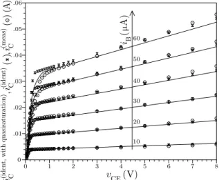
As shown in Figure 2, the saturation part of the characteristics is not optimally modeled. There-fore, the newer part of the equations for mod-eling the quasisaturation [6]must also be con-sidered. The results of such improved identi-fication are shown in Figure 4 (they are drawn using natural linear axes for a comparison with the previous logarithmic ones). The optimiza-tion determined the addioptimiza-tional model parame-tersrCO =10Ω, VO =100 V, and γ = 10−7.
With the inclusion of the quasisaturation model, the errors of the identification were lesser than those above: rms=3.51 % andδmax =14.9 %.
vCE( )V
i B
A
()
μ
0 1 2 3 4 5 6 7 8
0 .01 .02 .03 .04 .05 .06
10 20 30 40 50 60
A
i
i
i
C
(iden
t,
with
quasisatur
ation)
C
(iden
t)
C
(meas)
()
()
(
)
,
,
Figure 4.Using quasisaturation model of the BJT
KC508.
.5 .6 .7 .8 .9 1
1E-5 .0001 .001 .01 .1 1
0 10 20 30 40 50
vBE( )V
δ
(%)
ii B
(iden
t)
B
(meas)
(
)
(A)
,
Figure 5.Forward input characteristic of the BJT
The parameters of the nonlinear base-resistance model were identified using the input character-istic of the transistor as shown in Figure 5. The input characteristic was identified with the er-rors rms=13.5 % andδmax = 35.0 % and the optimization determined the model parameters
rB = 26Ω, rBM = 37 mΩ, IrB = 3.4μA, and
rE =0.53Ω.
The parameters of the dynamic part of the model were also identified. First, both junction ca-pacitances were determined as shown in Fig-ure 6. The identification had the errors rms = 1.57 %(E),1.64 %(C)andδmax =2.51 %(E), 2.73 %(C), and the optimization gave the model parameters CJE = 4.38 pF, φE = 0.65 V,
mE = 0.4, CJC = 3.11 pF, φC = 0.4 V, and
mC = 0.273. Second, the transit-time model
0 .5 1 1.5 2 2.5 3 3.5
1 2 3 4 5 6
cc
cc
E
(iden
t)
E
(meas)
C
(iden
t)
C
(meas)
()
(
)
(pF)
,
,,
cE
cC
0 2. −vBE,0 2. −vBC(V)
Figure 6. Collector and emitter junction capacitances of
the BJT KC508.
0 .2E-6 .4E-6 .6E-6 .8E-6 1E-6
-.02 0 .02 .04 .06 .08 .1
t(s)
iiE
(iden
t)
E
(meas)
(
)
(A)
,
Figure 7.Identification of transit-time model parameters
of the BJT KC508.
parameters were identified as shown in Fig-ure 7. The optimization determined the model parameters τF = 0.249 ns, IτF = 0.35 A,
VτF = 8.52 V, and XτF = 0.33 with the er-rors rms = 31.8 % and δmax = 94.4 %. The last two ones seem to be large – however, the differences were determined using the “verti-cal” distances which were not optimal here, of course(actually, the identification can be con-sidered quite successful). The reverse transit time was identified in the same way with the resultτR =23 ns.
High Frequency Transistor. The second iden-tified BJT was the microwave KT391 with the characteristics shown in Figure 8. The irreg-ularities were probably caused by oscillations during the measurement – it was very difficult
vCE( )V
iB
A
()
μ
.01 .02 .05 .1 .2 .5 1 2 5 10
100
90 80
70 60
50
40
30
20
10
0 .001 .002 .003 .004 .005 .006 .007
ii C
(iden
t)
C
(meas)
A
,(
)(
)
Figure 8.Forward DC characteristics of the microwave
BJT KT391.
δ
(%)
.1 .2 .5 1 2 5 10
0 5 10 15 20 25
0 .001
.002 .003
.004 .005
iC (iden
t) (A )
vCE ( )V
Figure 9.Relative errors of the identification in the
to perform the DC measurements for the mi-crowave transistors due to problematic stability.
The optimization determined the values of the model parameters IS = 10−8 A, ISE = 4.7×
10−9 A, I
SC = 10−7 A, βF = 133, βR = 1.6,
nF = 1.15,nR = 1.13, nE = 1.86,nC = 1.75,
VAF =123 V,VAR =2 V,IKF =18 mA,IKR =
86 mA, rC = 2 Ω, rB = 10 Ω, rBM = 1 Ω,
IrB=100μA, andrE =1.6Ωwith the
identifi-cation errors rms=16.0 % andδmax =61.7 %. However, if only the triangular “stable” region was used, as shown in Figures 8 and 9, then the identification errors were lesser: rms=5.99 % andδmax =22.2 %.
-12 -10 -8 -6 -4 -2 0
-6
-7
-8
-9
-10 -.006
-.005 -.004 -.003 -.002 -.001 0
vGS
V()
vDS(V)
iiD
(iden
t)
D
(meas)
(
)
(A)
,
Figure 10.Forward DC characteristics of the P-channel
enhancement-mode MOSFET 2N3608.
vDS(V)
vGS( )V
iiD
(iden
t)
D
(meas)
(
)
(A)
,
.1 .2 .5 1 2 5 10
3.85
3.8
3.75
3.7
3.6
3.5
0 .25 .5 .75 1 1.25 1.5 1.75 2
Figure 11.Forward DC characteristics of the N-channel
enhancement-mode MOSFET BUZ345.
3.2. MOSFET
Enhancement Mode Transistors. At first, let us identify the models of enhancement-mode transistors. The first one was the low-power P-channel MOSFET 2N3608 – see Figure 10. The identification procedure determined the values of the model parameters VTO = −4.77 V,
φS = 0.657 V, φO = 0.806 V, W = 37.9μm,
L=3.46μm,XJ =1.54μm,XJL =0.762μm,
tox = 98.7 nm, NFS = 1015 m−2, NA =
2.32×10²²m−3,v
max =3.55×10⁵m/s,μO=
0.0719 m2/(Vs),EP=3.4 MV/m,κ =0.441,
KP = 2.49 × 10⁻⁵ A/V2, γ = 0.294 √V,
δ = 0.989, η = 0.03, θ = 0.00334 V−1, and ι = 0.34 (the last one was present only in the C.I.A. program where it served as an
ad-iiD
(iden
t)
D
(meas)
(
)
(A)
,
vDS(V)
v GS
V()
-0.75 -0.5 -0.25
0.250.5
0.75 1.25 1
0
-1
.1 .2 .5 1 2 5 10
.0001 .0002 .0005 .001 .002 .005 .01
Figure 12. Forward DC characteristics of the N-channel
depletion-mode MOSFET KF521.
0 1 2 3 4 5 6 7 8
1 1.25 1.5 1.75 2 2.25 2.5
cc
cc
S
(iden
t)
S
(meas)
D
(iden
t)
D
(meas)
()
(
)
(pF)
,
,,
−vBS,−vBD(V)
cS
cD
Figure 13.Drain and source junction capacitances of the
ditional fitting factor). The parameters of the model were found with the excellent precision: rms=2.18 % andδmax =5.41 %.
The second one was the high-power N-channel VMOS BUZ345 – see Figure 11. The iden-tification procedure determined the values of the model parameters VTO = 3.26 V, φS =
0.578 V, φO = 0.801 V, W = 1.46 m, L =
4.97 μm, XJ = 0.289 μm, XJL = 0.179 μm,
tox = 74.7 nm, NFS = 1015 m−2, NA =
1.73 × 10²⁰ m−3, v
max = 3.23 × 10⁵ m/s,
μO = 0.0585 m2/(Vs), κ = 0.0306, KP =
4.19×10⁻⁵ A/V2, γ = 0.366 √V, δ = 1,
θ = 0.0384 V−1, ι = 0.572, rD = 0.0249Ω,
andrS =0.0435Ω(for the power devices, the
drain and source resistances must also be identi-fied; in the previous example, their values were fixed to the defaults 10Ω). The identification errors for that power device were greater than those for the previous one (which is natural): rms= 8.67 % andδmax = 28.8 %. Moreover, the value ofWwas extreme but logical – power devices were composed of many single struc-tures and therefore such value represented an integral.
Depletion Mode Transistor. Let us identify the model of a depletion-mode transistor which was the N-channel KF521 – see Figure 12. The identification procedure determined the values of the model parametersVTO =−1.48 V,φS =
0.334 V, φO = 0.789 V, W = 443 μm, L =
4.83 μm, XJ = 0.932 μm, XJL = 0.827 μm,
tox = 71.8 nm, NFS = 1015 m−2, NA =
7.51 × 10²¹ m−3, vmax = 1.71 × 10⁵ m/s,
μO = 0.0535 m2/(Vs), EP = 419 kV/m,κ =
0.4,KP = 2.12×10⁻⁵A/V2, γ =0.568√V,
δ =1,η =0.811,θ = 0.002 V−1, ι =0.929,
rD=11.8Ω, andrS =5.17Ω. Again, the
iden-tification ended with small errors rms=4.06 % andδmax =14.5 %.
For the MOSFET KF521, the parameters of the model of its junction capacitances were also identified – see Figure 13. The identifica-tion procedure determined the model parame-tersCJOareaS =2.17 pF,CJOareaD=1.57 pF,
CJOswperimeterS =0.26 pF,CJOswperimeterD
= 0.182 pF, φO = 0.789 V, φOsw = 0.789 V,
mS = 0.302, mSsw = 0.183, mD = 0.213, and
mDsw = 0.286 – again, the errors of the iden-tification were relatively very small: rms =
-15 -12.5 -10 -7.5 -5 -2.5 0
0
1
2 0.5
1.5
1E-5 2E-5 5E-5 .0001 .0002 .0005 .001 .002 .005 .01
vGS
V(
)
vDS(V)
−
−
i
i
D
(iden
t)
D
(meas)
(
)
(A)
,
Figure 14.Forward DC characteristics of the P-channel
JFET 2N2498.
2.73 %(S), 3.15 %(D), andδmax =4.36 %(S), 6.90 %(D).
3.3. JFET
Let us identify the model parameters of the P-channel JFET 2N2498 – see Figure 14. The identification procedure determined the values of the model parametersVT = −2.288 V(i.e.,
the “physical” threshold voltage was+2.288 V
[6]),β =1.299×10⁻³A V−2,λ =0.02322 V−1,
rD=55.75Ω, andrS =108.3Ωwith the errors
rms =10.4 % andδmax =42.38 %(the larger
δmax occurred for the voltages/currents near to zero, which is far from the standard JFET opera-ting points).
4. Conclusion
5. Acknowledgments
This paper was supported by the grant of the Eu-ropean Commission TARGET (Top Amplifier Research Groups in a European Team), by the Grant Agency of the Czech Republic, grant No 102/05/0277, and by the Czech Technical Uni-versity Research Project MSM 6840770014.
References
[1] M. BUCHER, C. LALLEMENT, C. C. ENZ, An
Ef-ficient Parameter Extraction Methodology for the EKV MOST Model.In IEEE International
Confer-ence on Microelectronic Test Structures,(1996).
[2] T. COLEMAN, Y. ZHANG,Optimization Toolbox for
Use with MATLAB, User’s Guide. The
Math-Works, Inc., 2nded., 2003.
[3] R. FLETCHER, Practical Methods of Optimization.
John Wiley & Sons, 1978.
[4] L. FINSCHI, An implementation of the
Levenberg-Marquardt algorithm. Eidgen¨ossische Technische Hochschule Z¨urich, 1996.
[5] A. VLADIMIRESCU,The SPICE Book. John Wiley &
Sons, 1994.
[6] G. MASSOBRIO, P. ANTOGNETTI,Semiconductor
De-vices Modeling With SPICE. McGraw-Hill, 1993.
Received:June, 2007
Accepted:September, 2007
Contact addresses:
Josef Dobesˇ
Dept. of Radioelectronics Czech Technical University in Prague Technick´a 2, 166 27 Praha 6 Czech Republic e-mail:[email protected]
Martin Gr´abner Dept. of Radioelectronics Czech Technical University in Prague Technick´a 2, 166 27 Praha 6 Czech Republic e-mail:[email protected]
Lubom´ır Hruskoviˇ ˇc Dept. of Electromagnetic Field Czech Technical University in Prague Technick´a 2, 166 27 Praha 6 Czech Republic e-mail:[email protected]
JOSEFDOBEˇSreceived the Ph.D. degree in microelectronics from the Czech Technical University in Prague in 1986. From 1986 to 1992, he was a researcher of TESLA Research Institute where he performed analyses on algorithms for CMOS Technology Simulators. He is cur-rently with the Department of Radio Engineering of the Czech Techni-cal University in Prague. His current research interests include physiTechni-cal modeling of elements of electronic circuits, especially radio-frequency and microwave transistors and transmission lines, creating or improving special algorithms for circuit analysis and optimization such as time-and frequency-domain sensitivity, poles-zeros or steady-state analyses, and creating a comprehensive CAD tool for analysis and optimization of radio-frequency circuits.
MARTINGRABNER´ received the B.S. and M.S. degrees in electrical en-gineering from the Czech Technical University in Prague in 1998 and 2000, respectively. He has been with the Dept. of Microwave Commu-nications, TESTCOM. His work is focused on the propagation of radio waves in the atmosphere. He is also interested in circuit modelling of microwave transistors and optimization techniques.