Signature of Fermi-surface anisotropy in point contact conductance in the presence of defects
Ye. S. Avotina,1,2Yu. A. Kolesnichenko,1,2A. F. Otte,2and J. M. van Ruitenbeek2
1B.I. Verkin Institute for Low Temperature Physics and Engineering, National Academy of Sciences of Ukraine, 47, Lenin Ave.,
61103, Kharkov, Ukraine
2Kamerlingh Onnes Laboratorium, Universiteit Leiden, Postbus 9504, 2300 Leiden, The Netherlands 共Received 3 April 2006; published 16 August 2006兲
In a previous paper关Avotinaet al., Phys. Rev. B 71, 115430共2005兲兴we have shown that in principle it is possible to image the defect positions below a metal surface by means of a scanning tunneling microscope. The principle relies on the interference of electron waves scattered on the defects, which give rise to small but measurable conductance fluctuations. Whereas in that work the band structure was assumed to be free-electron like, here we investigate the effects of Fermi surface anisotropy. We demonstrate that the amplitude and period of the conductance oscillations are determined by the local geometry of the Fermi surface. The signal results from those points for which the electron velocity is directed along the vector connecting the point contact to the defect. For a general Fermi surface geometry the position of the maximum amplitude of the conductance oscillations is not found for the tip directly above the defect. We have determined optimal conditions for determination of defect positions in metals with closed and open Fermi surfaces.
DOI:10.1103/PhysRevB.74.085411 PACS number共s兲: 73.23.⫺b, 72.10.Fk
I. INTRODUCTION
The interference of electron waves scattered by single de-fects results in an oscillatory dependence of the point contact conductanceG共V兲on the applied voltageV. This effect origi-nates from quantum interference between the principal wave that is directly transmitted through the contact and the partial wave that is scattered by the contact and the defect or several defects. Such conductance oscillations have been observed in quantum point contacts1–4 and investigated theoretically in the papers.3,5–7
In our previous paper8the oscillatory voltage dependence of the conductance of a tunnel point contact in the presence of a single pointlike defect has been analyzed theoretically and it has been shown that this dependence can be used for the determination of defect positions below a metal surface by means of a scanning tunneling microscope共STM兲. In the model of a spherical Fermi surface共FS兲the amplitude of the conductance oscillations is maximal when the contact is placed directly above the defect. The oscillatory part of the conductance⌬Gfor this situation is proportional to
⌬G共V兲 ⬃sin
冉
2z0冑
kF2
+2meV ប2
冊
,wherez0the depth of the defect andkFandmare the Fermi
wave vector and effective mass of the electrons.8 Materials with an almost spherical FS are most suitable for this model. In most metals the dispersion relation for the charge car-riers is a complicated anisotropic function of the momentum. This leads to anisotropy of the various kinetic characteristics.9Particularly, as shown in Ref.10, the current spreading may be strongly anisotropic in the vicinity of a point contact. This effect influences the way the point contact conductance depends on the position of the defect. For ex-ample, in the case of a Au共111兲surface the necks in the FS should cause a defect to be invisible when probed exactly from above.
Qualitatively, the wave function of electrons injected by a point contact for arbitrary FS共p兲=Fhas been analyzed by
Kosevich.10He noted that at large distances from the contact the electron wave function for a certain directionris defined by those points on the FS for which the electron group ve-locity is parallel tor. Unless the entire FS is convex there are several such points. The amplitude of the wave function de-pends on the Gaussian curvatureKin these points, which can be convex 共K⬎0兲 or concave 共K⬍0兲. The parts of the FS having different signs of curvature are separated by lines of
K= 0共inflection lines兲. In general there is a continuous set of electron wave vectors for which K= 0. The electron flux in the directions having zero Gaussian curvature exceeds the flux in other directions.10
Electron scattering by defects in metals with an arbitrary FS can be strongly anisotropic.9Generally, the wave function of the electrons scattered by the defect consists of several superimposed waves, which travel with different velocities. In the case of an open constant-energy surface there are di-rections along which the electrons cannot move at all. Scat-tering events along those directions occur only if the electron is transferred to a different sheet of the FS.9
com-mon features of FS geometries to the conductance oscilla-tions: anisotropy of a convex part共bellies兲, changing of the curvature共inflection lines兲 and presence of open directions 共necks兲.
II. THE SCHRÖDINGER EQUATION FOR QUASIPARTICLES
Let us consider as a model for our system a nontranspar-ent interface located atz= 0 separating two metal half-spaces, in which there is an orifice共contact兲of radiusRcentered at the pointr= 0. The potential barrier in the planez= 0 is taken to be a delta function,
U共r兲=Uf共兲␦共z兲, 共1兲
where=共x,y兲 is a two-dimensional vector in the plane of the interface, with r=共,z兲. The function f共兲→⬁ in all points of the plane z= 0 except in the contact, where f共兲
= 1. At the point r=r0 near the contact in the upper half-space,z⬎0, a pointlike defect is placed. The electron inter-action with the defect is described by the potential D共r
−r0兲, which is confined to a small region with a characteris-tic radiusrDaround the pointr0.
It is known that one can obtain an effective Schrödinger equation for quasiparticles in a metal from the dispersion relation共p兲 共the band structure兲by replacement of the qua-simomentump 共below for short we write momentum兲in the function共p兲with the momentum operatorpˆ =បiⵜ.9Here we do not specify the specific form of the dependence 共p兲, except that it satisfies the general condition of point symme-try共p兲=共−p兲. For simplicity we assume that FS has only one sheet; there is only one zone described by the function 共p兲. In the reduced zone scheme a given momentump iden-tifies a single point within the first Brillouin zone. The wave function共r兲satisfies the Schrödinger equation with an ef-fective Hamiltonian共pˆ兲,
共pˆ兲共r兲+关−U共r兲−eV共z兲兴共r兲=D共r−r0兲共r兲, 共2兲 whereU共r兲is defined by Eq.共1兲,V共z兲is the applied electri-cal potential, andis the electron energy.
We consider a large barrier potentialU. In this case the amplitudetof the electron wave function passing through the barrier is
t共,pt兲 ⬇
ប共vzin−vzref兲
2iU , 共3兲
where vz
in and vz
ref
are the z components of the velocity v
=共p兲/pof incident electrons共in兲and electrons specularly reflected by the barrier共ref兲, respectively. Under condition of specular reflection the energy and the component of the momentum tangential to the interface,pt=共px,py兲atz= 0 are
conserved. The components of the electron momentum per-pendicular to the interface, pzin共pt,兲 and pzref共pt,兲 are
re-lated by the equations, 共pt
in ,pz
in兲 =共pt
ref ,pz
ref兲
=, pt
in =pt
ref⬅
pt. 共4兲
The velocitiesvzinandvzrefhave the opposite sign
vin·N⬍0, vref·N⬎0, 共5兲
whereNis a unit vector normal to the interface laying in the half-space of the electron wave under consideration 关N
=共0 , 0 , 1兲 forz⬎0 andN=共0 , 0 , −1兲 for z⬍0兴. We will as-sume that the crystallographic axes in half-spaces z0 are identical. In this case the momenta and velocities for elec-trons incident on the barrier and for those transmitted through the barrier are equal.
In general Eq.共4兲may have several solutions, i.e., several specularly reflected states may correspond to an incident state with momentum pzin. Such reflection is called
multi-channel specular reflection.11Below we assume that there is only one reflected electron state.
In the limit of a small probability of electron tunneling through the barrier,兩t兩2Ⰶ1 the applied voltage drops entirely over the barrier and we take the electric potential to be a step functionV共z兲=V⌰共−z兲. The reference point of zero electron energy is the bottom of the conduction band in the upper half-space, z⬎0. The conduction band in the lower half-spacez⬍0 is shifted by a valueeV. We also assume that the applied biaseVis much smaller than the Fermi energy and in solving the Schrödinger Eq. 共2兲 we neglect the electric po-tentialV共z兲. Equation共2兲can be solved by using perturbation theory with the small parameter 兩t兩Ⰶ1.12 In the zeroth ap-proximation in this parameter we have the problem of an impenetrable partition between two metal half-spaces.
We start by solving for the wave function共0兲共,p
t;r兲for
a tunneling point contact of low transparency,兩t兩Ⰶ1 without defects 关D共r−r0兲= 0兴. The wave function 0共0兲共r兲, in zeroth order in the parameter 兩t兩Ⰶ1, satisfies the boundary condi-tion0共0兲共z= 0兲= 0 at the interface,
0共0兲共,pt;r兲=eipt/ប共eipz
inz
/ប−eipzrefz/ប兲. 共6兲 Let us consider an electron wave exp共ipr/ប兲 incident on the junction from the lower half-spacez⬍0, so thatvz⬎0. In
this half-space to first approximation in the parameter t the solution 共0兲共r兲 of the homogeneous Schrödinger equation can be written in the form12
共0兲共r兲= 0
共0兲共r兲+共−兲共r兲, z⬍0, 共7兲 where the second term,共−兲共r兲⬀t, describes the changes in the reflected wave as a result of transmission through the contact. The wave function transmitted into the half-space
z⬎0 is proportional to the amplitude t,
共0兲共r兲=共+兲共r兲, z⬎0. 共8兲 The function 共0兲共,z兲 satisfies the condition of continuity and the condition of conservation of probability flow at z
= 0. For small兩t兩these conditions reduce to
共−兲共,0兲=共+兲共,0兲, 共9兲
teipt/ប=f共兲共+兲共,0兲. 共10兲
共+兲共,z兲=t
冕
−⬁ ⬁ dp
t
⬘
共2ប兲2F共pt−pt
⬘
兲ei关pt⬘+pz共+兲共,pt⬘兲z兴/ប, 共11兲 where
F共pt−pt
⬘
兲=冕
−⬁ ⬁
de
i共pt−pt⬘兲/ប
f共兲 ; 共12兲
pz共±兲共,pt
⬘
兲are roots of the equation共pt
⬘
,pz共±兲兲=共p兲, 共13兲corresponding to waves with velocities vz共+兲共,pt
⬘
兲⬎0 and vz共−兲共,pt⬘
兲⬍0.LetD共r兲 be a spherically symmetric scattering potential for a pointlike defect, with a range rD that is order of the
Fermi wavelength F 关DⰆD共0兲, the maximal value of D,
when兩r−r0兩ⰇrD兴. For a pointlike defect共rD→0兲, the
right-hand side in the Schrödinger Eq. 共2兲 can be rewritten as
D共r−r0兲共r0兲.13This makes it possible to find a solution to Eq. 共2兲 by means of the Green function G0+共r
⬘
,r;兲 of the homogeneous equation 共at D= 0兲. The wave function scat-tered from the defect,共r兲, can be expressed in terms of the wave function共+兲共r兲transmitted into the upper metal half-space,共r兲=共+兲共r兲+共+兲共r0兲 J共r,r0兲
1 −J共r0,r0兲
, 共14兲
where
J共r,r0兲=
冕
dr⬘
D共r⬘
−r0兲G0+共r⬘
,r;兲. 共15兲Because the Green function has a singularity at r→r
⬘
, Eq. 共14兲 is correct if the integralJ共r,r0兲 共15兲 converges in the pointr=r0.To proceed with further calculations we assume that the scattering potential is small and use perturbation theory in the interaction with the defect. This implies that we take 兩J共r0,r0兲兩Ⰶ1. The wave function solution, that is linear in兩t兩
and with a contribution to first order inD, is
共r兲=共+兲共r兲+共+兲共r0兲
冕
dr⬘
D共r⬘
−r0兲G0+共r,r⬘
;兲. 共16兲 The Green functionG0共r,r⬘
;兲 in zeroth approximation in the parametersDand兩t兩should be calculated from the wave functions共6兲,G0+共r,r
⬘
;兲=冕
dp 共2ប兲30共0兲共r兲关0共0兲共r
⬘
兲兴*−共p兲−i0 . 共17兲 This is the Green function of the Schrödinger equation in the half-spacez⬎0 with hard-wall boundary conditions atz= 0. Substituting the wave function0共0兲共r兲, Eq. 共6兲, for z⬎0 in Eq.共17兲, we find
G0+共r,r
⬘
;兲= 1iប
冕
dpt
共2ប兲2
eipt共−⬘兲/ប+ipz共
+兲z/ប
vz共
+兲 −vz共
−兲 共e −ipz共+兲z⬘/ប −e−ipz共
−兲z⬘
/ប兲, z⬎z
⬘
. 共18兲For 0⬍z⬍z
⬘
one should make the replacementsz↔z⬘
andpz共−兲↔−pz共+兲 in Eq.共18兲; pz共±兲are given by Eq.共13兲.
The main contribution to the integral in Eq. 共16兲 comes from a small region near the pointr
⬘
=r0. Far from the pointr=r0共兩r−r0兩ⰇrD兲the solution共16兲takes the form
共r兲=共+兲共r兲+gG0+共r,r0;兲共+兲共r0兲, 共19兲 where
g=
冕
dr⬘
D共r⬘
−r0兲 共20兲is the constant of electron-impurity interaction.
III. POINT-CONTACT CONDUCTANCE
The electrical currentI共V兲can be evaluated from the elec-tron wave functions,, of the system through14
I共V兲= 2e
共2ប兲3
冕
dpIp⌰共vz兲关nF共兲−nF共+eV兲兴. 共21兲Here
Ip=
冕
−⬁ ⬁
dxdyRe共*vˆ
z兲 共22兲
is the density of probability flow in the z direction for the momentump, integrated over a planez=xconst,nF共兲is the
Fermi distribution function, and vˆ is the velocity operator,
vˆ =共pˆ兲/pˆ . For the definiteness we choose in Eq.共21兲eV
⬎0. At low temperatures the tunnel current is due to those electrons in the half-spacez⬍0 having an energy between the Fermi energy,F, and F+eV, because on the other side
of the barrierz⬎0 only states with艌F are available.
After performing the integration over a plane at zⰇz0, where the wave function共19兲can be used, we find the den-sity flow共22兲becomes
Ip=兩t共,pt兲兩23បR4具共vz共
+兲兲2典 共兲
+兩t共,pt兲兩 2g2R4
ប Re
冕
dpt
⬘
共2ប兲2
ivz共
+兲共p
t
⬘
兲e−ipt⬘0/ប vz共+兲共p
t
⬘
兲−vz共−兲共p
t
⬘
兲 ⫻共e−ipz共+兲共p
t
⬘兲z0/ប−e−ipz共−兲共pt⬘兲z0/ប兲
⫻
冕
−⬁ ⬁ dp
t
⬙
共2ប兲2e
具¯典=
冕
p=dSp
兩v兩 ¯
冕
p=dSp
兩v兩
, 共24兲
scaled by the velocity, 兩v兩=兩p兩. In Eq. 共23兲, pz共+兲共pt兲 and pz共−兲共pt兲are given by Eq.共13兲and共兲is the electron density
of states per unit volume.
Taking into account Eq.共23兲we can calculate the current-voltage characteristics I共V兲. The conductance G共V兲 is the first derivative of the currentI共V兲withV and in the limitT
→0 we obtain
G共V兲= I V=e
2共兲具I
p典F+eV. 共25兲
After integration overSp共24兲, Eq.共25兲should be expanded
in the parametereV/FⰆ1.
IV. ASYMPTOTICS OF THE WAVE FUNCTION AND THE CONDUCTANCE
In this section we find the wave function at large distances from the contact, rⰇF, and an asymptotic expression for
the conductance in the limit of a large distance between the defect and the contact, r0ⰇF and a small contact radius, RⰆF, whereF is the characteristic electron Fermi
wave-length. ForR→0 the functionFin Eq.共12兲takes the form8
F共pt−pt
⬘
兲=R2, 共26兲and the wave function共11兲can be written as
共+兲共,z兲=t共,p
t兲R2
冕
−⬁ ⬁ dp
t
⬘
共2ប兲2e
i关pt⬘+pz共+兲共pt⬘兲z兴/ប. 共27兲 Let us consider the integral
⌳共r,兲=
冕
−⬁⬁ dp
t
⬘
共2ប兲2e
i⌫共pt,r兲
, 共28兲
where⌫共pt,r兲 is the phase accumulated over the path
trav-eled by the electron between the contact and the pointr,
⌫共pt,r兲=
1
ប关pt+pz共
+兲共p
t兲z兴. 共29兲
This kind of integral appears in the expressions for the wave function关Eqs.共27兲,共18兲, and共19兲兴and for the conductance 关Eqs.共23兲and共25兲兴. At a large distance,rⰇF, the exponent
under the integral in Eq.共28兲is a rapidly oscillating function and the integral can be calculated by the stationary phase method 共see, for example, Ref. 15兲. The stationary phase pointspt=pt
共st兲
are defined by the equation
冏
⌫ pt冏
pt=pt
共st兲= 0. 共30兲
With Eq.共29兲we find
+z
冏
pz共+兲共p
t兲
pt
冏
pt=p t共st兲
=−z
冏
vt共+兲共p
t兲
vz共pt兲
冏
pt=p t共st兲 = 0.
共31兲 ForrⰇFthe asymptotic value⌳as共r,兲of the integral共28兲
is given by
⌳as共r,兲= cos
2បr
冑
兩K0兩exp冋
i⌫0+i 4 sgn
冉
2pz
px共
st兲2
冊
共1+ sgnK0兲
册
. 共32兲Here
⌫0共,r兲=⌫共pt共
st兲
,r兲 共33兲
is the phase共29兲in a point defined by Eq.共31兲,K共,p兲is the Gaussian curvature of the surface of constant energy 共px,py,pz兲=, and cos共r兲=z/r is the angle between the
vector r and the z axis. At the stationary phase points the curvatureK共,p兲can be written as
K0共,n兲=
冉
1兩v兩2i,k
兺
=x,y,zAiknink
冊
pt=pt
共st兲
, 共34兲
whereAik=
det共m−1兲
mik−1共p兲 is the algebraic adjunct of the element
mik
−1共
p兲=
2 pipk
共35兲
of the inverse mass matrixm−1;16 n
iare components of the
unit vectorn=r/r. Note that for an arbitrary FSmik共p兲in the
pointpt=pt
共st兲
depends on the direction of vectorr. It follows from Eq.共31兲that the velocity at the stationary phase point
pt共st兲 is parallel to the radius vectorr=共,z兲.
If the curvature of the FS changes sign, Eq.共31兲has more than one solutionpt=pt,s
共st兲共s= 1 , 2 , . . .兲. In that case the value
of the integral共28兲is replaced by a sum over all pointspt共,sts兲, which in the limit of large distances is
⌳共r,兲 ⬇
兺
s
⌳sas共r,兲, 共36兲
with ⌳sas共r,兲 given by Eq. 共32兲 for each stationary phase points. It may also occur that Eq. 共31兲 does not have any solution for given directions of the vectorr, and the electron cannot propagate along these directions. These two energy surface properties result in complicated patterns of the dis-tribution of the modulus of the wave function:共1兲For direc-tions for which Eq. 共31兲 has several solutions a quantum interference pattern of the electron waves with different ve-locities should be observed.共2兲When Eq.共31兲has no solu-tion for the selected direcsolu-tion of the vectorrclassical motion in this direction is forbidden and the wave function is expo-nentially small.
For large valuesr,r
⬘
ⰇFthe asymptotic behaviors of theGreen function, Eq.共18兲, and of the conductance, Eq.共25兲at
r0ⰇF, can be found analogous to the evaluation of the
mo-mentum must be taken in the stationary phase point. For the partial wave scattered by the defect that is moving towards the interface pz共+兲共pt兲 in Eq. 共29兲 must be replaced by pz共−兲共pt兲. In this case the stationary points have a group
ve-locity v共−兲 directed from the point r0 towards the contact. From the central symmetry of the FS,共p兲=共−p兲, it follows that the two stationary phase points for the function⌫共pt,r兲
are antiparallel,p共+兲共st兲= −p共−兲共st兲⬅p共st兲.
Next, we derive an asymptotic expression for the wave function 共19兲, with r,兩r−r0兩ⰇF, for a symmetric
orienta-tion of the FS with respect to the interface, so that vz共+兲= −vz共−兲,pz共+兲= −pz共−兲andmik
−1
= 0, ifi⫽k. Under these conditions the wave function共19兲takes the form
共r兲 ⬇共+兲共r兲+ gi 4ប
共+兲共r0兲
兺
s
冉
1 vz共+兲共pt共,1s兲兲
⌳s
as共 −0,z
+z0;兲− 1 vz共+兲共pt共,2s兲兲
⌳s
as共
−0,兩z−z0兩;兲
冊
, 共37兲with
共+兲共r兲 ⬇tR2
兺
s
⌳s
as共
r,兲. 共38兲
In Eq.共37兲the velocityvz共+兲is taken in the stationary phase pointspt共st兲=pt共,1,2s 兲corresponding to the directions of the vec-tor with coordinates共−0,兩z±z0兩兲.
We have assumed for the Gaussian curvature, Eq. 共34兲, that K0⫽0 in the stationary phase points pt
共st兲
. For those points at whichK0= 0 the integral共28兲diverges. This means that the third derivative of the phase ⌫共pt,r兲 共29兲 with
re-spect toptmust be taken into account. In Sec. V this is done
for a model FS having cylindrical symmetry with respect to an open direction. Here we only note that the amplitude of the wave function共+兲共r兲 共38兲in a direction of zero Gaussian curvature is larger than for other directions, and decreases more slowly as compared to the ⬃1 /r dependence of Eq. 共32兲. This results in an enhanced current flow near the cone surface defined by the condition K0= 0.10 The same effect also appears in the second term of the wave function共37兲, that describes the scattered wave: the amplitude of this par-tial wave is maximal in the directions of zero Gaussian cur-vature.
If the FS has a flat part, i.e., Eq.共31兲holds at all points of a FS region of finite areaSfl, the associated electron waves propagate in the metal without decrease of their amplitude.10 For the flat part the dispersion relation共p兲can be presented as 共p兲=v0p, where v0= const is the electron velocity. For such FS the asymptotic value of the integral共28兲is
⌳fl as共
r,兲= v0zSfl
兩v0兩共2ប兲2exp
冉
ir
ប兩v0兩
冊
. 共39兲When the distance between the contact and the defect is large,r0ⰇF, we obtain the conductance of the tunnel
junc-tion, using Eq. 共23兲 and the asymptotic expression for the wave function共37兲,
G=G0
冉
1 −g
2ប2具共vz共
+兲兲2典 F共F兲
⫻
兺
s,s⬘
Re⌳s
as共
r0,F,eV兲
⫻Im⌳s⬘
as共
r0,F,eV兲
冊
, 共40兲whereG0is the zero-bias共eV→0兲conductance of the junc-tion without defect,
G0=e23R4ប具兩t兩2典F
2共
F兲具共vz共
+兲兲2典
F. 共41兲
In deriving Eq. 共40兲 we have assumed that eVⰆF and r0 ⰇF. Therefore, all functions of the energyin Eq.共40兲can
be taken at =F, except for the phase ⌫0共,r兲. When eV
ⰆF,
⌫0共r0,F+eV兲 ⬇⌫0共F兲+
⌫0 F
eV, ⌫0
F
⬃ 1 F
r0 F
共42兲
and when the product共eV/F兲共r0/F兲Ⰷ1 clearly the
conduc-tance共40兲 is an oscillatory function of the voltage V. Note that if the inequalityeVⰆFis not satisfied, the value of the
conductance共41兲as well as the amplitude of its oscillations depend onV. The periods of oscillations are defined by the energy dependence of the function⌫0共,r0兲and they remain the same for any voltage. Below presenting formulas for the conductance in different cases we do not expand arguments of oscillatory functions in the parametereV/F. The obtained
results properly describe the total conductance ateVⰆFand
also can be used for the analysis of periods of oscillations at
eV艋F. In Eq.共40兲the ⌳s
as共r
0,F,eV兲 denotes the function
共32兲, in which⌫0=⌫0共r0,F+eV兲. Equation共40兲shows that
for a tunnel junction of small size the amplitude and period of conductance oscillations depend on the local geometry FS in those points for which the velocity is directed along the vectorr0.
In the case of a convex FS there is only one stationary phase point satisfying Eq.共31兲which allows simplifying the expression for the conductance共40兲. The oscillating part of the conductance,⌬G, can be written as
⌬G
G0
= g
2具共vz共+兲兲2典F共F兲共2ប兲3r02
冉
关vz共+兲共,pt兲兴2
兺
i,k=x,y,z
Aikn0in0k
⫻sin关2⌫0共r0,F+eV兲兴
冊
pt=p t
共st兲
, 共43兲
2⌫0共r0,兲= 2
បp共st兲r0, 共44兲
where 2兩p共st兲兩 is the chord connecting the two points on the surface of constant energy for which the velocities are anti-parallel and aligned with the vectorr0.
If the direction from the contact to the defect coincides with a direction of electron velocities for a flat part of the FS, we should use asymptotic expression 共39兲 for the function ⌳flas共r0,兲 when calculating the conductance 共40兲. For this case the oscillating part of the conductance,⌬G, is given by
⌬G
G0 =
gSfl2vz0 2 具共vz共
+兲兲2典 F兩v0兩
2共
F兲共2ប兲4
sin
冉
2共F+eV兲r0 ប兩v0兩冊
.共45兲 Note thatr0/兩v0兩=z0/vz0. In the case when the FS has a flat part, the amplitude of the conductance oscillations for those special directions does not depend on the distance between the contact and the defect.
In the next sections we shall consider two models of an-isotropic FSs. The first model, of an ellipsoidal FS, illustrates the main features of the conductance oscillations for metals with a convex FS, i.e., with positive Gaussian curvature. The FS of the second model has the shape of a corrugated cylin-der, which illustrates the effects of sign inversion of the cur-vature and the presence of open directions of the FS. These two models allow us to obtain dependencies of the conduc-tance on the applied voltage and on the defect position in analytical form.
V. ELLIPSOIDAL FERMI SURFACE
For an ellipsoidal FS the Schrödinger Eq.共2兲can, in fact, be solved exactly in the limitR→0 and the wave function 共19兲 and the conductance 共25兲 can be found for arbitrary distances between the contact and the defect. For this FS the dependence of the electron energy on the momentump is given by relation
共p兲=1 2i,k
兺
=x,y,zpkpi mik
; 共46兲
wherepi are the components of the electron momentump,
1 /mik are constants representing the components of the
in-verse effective mass tensorm−1. The tensor m−1 can be di-agonalized to the form 兵m−1其
ik=mi−1␦ik so that the
momentum-space lengths
冑
2Fmicorrespond to the semiaxesof the FS ellipsoid共p兲=F.
For the ellipsoidal FS in absence of a defect共zeroth ap-proximation兲the wave function共+兲共r兲 共27兲can be obtained by integration of Eq.共27兲over momentum,
共+兲共r兲=t共,p
t兲
冑
2共兲3/2zR2ប3
冑
detm−1ei⌫0关1 −i⌫0共r兲兴
⌫03共r兲
, 共47兲
where
⌫0共,r兲= r
ប
冑
2i,k兺
=x,y,ziknink, 共48兲
and
t共,pt兲=
ប
iUmzz
冑
2mzz−mzz
兺
i,k=x,ypipk mik
+
冉
mzz兺
i=x,ypi mzi
冊
2 . 共49兲 Here,ikare the elements of the mass tensor, which is the
inversive to the tensorm−1共m−1=I, withIthe unitary ten-sor; ik=Aik/ detm−1兲. The Green function 共18兲 takes the
form
G0+共r,r
⬘
;兲=2
冑
2 ប3冑
detm−1冢
exp
冉
i冑
⌫02共r−r⬘
兲+8mzzzz⬘
ប2
冊
冑
⌫02共r−r⬘
兲+8mzzzz
⬘
ប2
−exp关i⌫0共r−r
⬘
兲兴⌫0共r−r
⬘
兲冣
. 共50兲Using Eqs.共47兲and共50兲we obtain the wave function共19兲to first approximation in the strength of the impurity potential. The modulus of this wave function is illustrated in Fig.1for a plane normal to the interface passing through the impurity and the contact.
The conductance in the limit of low temperatures,T→0, is obtained from Eqs. 共23兲 and共25兲 by integration over all directions of the momentumpand integration over the space coordinatein a planez= const共z⬎z0兲, retaining only terms FIG. 1. Gray-scale plot of the modulus of the wave function in the planex= 0 for an ellipsoidal FS. The shape of the FS is defined by the mass ratios mx/mz= 1, my/mz= 3, and the long axis of the ellipsoid is rotated by/ 4 around thexaxis, away from theyaxis. The coordinates are measured in units ofz=ប/
冑
2mzz. The posi-tion of the defect isr0=共0 , 5 , 15兲. An interference pattern is visibleto first order in g 共i.e., ignoring multiple scattering at the impurity site兲,
Gell共V兲=G 0
ell
再
1 −12 2gz0 2共2
F兲3/2
ប5
冑
mzzdet共m−1兲
1 ⌫0
4共
F,r0兲
⫻
冋
1 2冉
1 −1 ⌫02共F,r0兲
冊
sin 2⌫0共F+eV,r0兲
+ 1
⌫0共F,r0兲
cos 2⌫0共F+eV,r0兲
册
冎
, 共51兲with⌫0共,r兲given by共44兲.
The amplitude of the conductance oscillations is maximal when⌫0is minimal. For a fixed depthz0 this minimum oc-curs when the defect position 0 is in the point 00 with respect to the point contact atr= 0, where
00=z0
冉
mzz/mzx mzz/mzy
冊
. 共52兲
The minimal value of the phase then becomes
⌫00=⌫0共F+eV,00,z0兲= 1
បz0
冑
2共F+eV兲mzz. 共53兲The phase⌫00corresponds to the extremal value of the chord of the FS in the direction normal to the interface.G0ellin Eq. 共51兲is the conductance in the absence of a defect共g= 0兲,
G0ell= 2e
2R4
F
3
9ប3U2
冑
det共m−1兲冑mzz
. 共54兲
Figure2 shows a plot of the oscillatory part of the
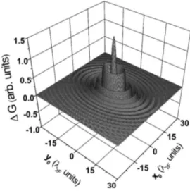
con-ductance, ⌬G=Gell共0兲−G 0
ell, Eq. 共51兲, for the contact as a function of the position of the defect,0, in the limit of low voltage,V→0.
For the ellipsoidal model FS the wave function and con-ductance have been obtained exactly, within the framework of the model. For large distancesrandr0they transform into the asymptotic expressions, Eqs. 共37兲 and 共40兲. We do not present the asymptotic form explicitly but it agrees to within a term proportional to⌫0−4to the exact from, Eq.共51兲. In Fig.
3we compare the results for the calculations of the conduc-tance by using the exact 共51兲 and asymptotic 共40兲 expres-sions. The figure confirms that for relatively small distances 关Fig. 3共a兲兴 the asymptotic formula still qualitatively de-scribes the conductance very well and that for larger dis-tances 关Fig. 3共b兲兴 the two results are in a good agreement. The parameters for the FS in Figs.2and3 are the same as those for Fig.1.
VI. OPEN FERMI SURFACE
The second model FS we want to discuss has the form of a corrugated cylinder共Fig.4兲, which is open along the direc-tionp储,
共p兲= p⬜ 2
2m+1sin
2p储b
2 , −
b 艋p储艋
b, ⬎ 1,
共55兲 where 2/b is the size of the Brillouin zone, andm is an effective mass. We further impose that the momentum per-FIG. 2. Dependence of the oscillatory part of the conductance,
⌬G, as a function of the position of the defect0in the plane z
=z0for the same shape and orientation of the ellipsoidal FS as in Fig.1. The coordinates are measured in unitszF=ប/
冑
2mzzFand the defect sits atz0= 5. The figure shows that⌬Gis an oscillatory function of the defect position that reflects the ellipsoidal form of the FS and the oscillations are largest when the defect is placed in the position00, defined by Eq.共52兲.FIG. 3. Comparison of the oscillating part of the conductance for an ellipsoidal FS calculated in the point0共52兲of the maximum
amplitude by using the asymptotic共dashed curve兲and exact共solid curve兲formulas. The depths of the defect arez0= 4共a兲and z0= 10
pendicular to the symmetry axis of the FS remains finite,
p⬜max艋p⬜艋p⬜min, 共56兲
where
p⬜max共兲=
冑
2m, p⬜min共兲=冑
2m共−1兲 共57兲are the maximal and minimal radii of the cylindrical surface, respectively. As a consequence of rotational symmetry the Gaussian curvature K 共34兲 of the surface depends only on
p⬜. The central part of the surface 共belly兲 has a positive curvature K⬎0 while the ends near the Brillouin zone boundary共necks兲 have negative curvature. In the direction perpendicular to the symmetry axis there are two partial waves propagating with different parallel velocities,v1 and
v2, belonging to the parts of FS having opposite sign of K. Rotating away from the perpendicular direction towards the axis the two solutions persist but the two corresponding points on the FS move closer together until they merge at the curve defined byK= 0, the inflection line. For directions be-yond this angle 共i.e., for ⬍c in Fig. 4兲 no propagating
wave solutions exist. On the inflection line a unique solution with velocityvcis found. For⬎cthere are two stationary
phase pointsp⬜s共s= 1 , 2兲that satisfy Eq.共31兲, corresponding
with two different velocitiesv共+兲共p
⬜s兲directed along the
ra-dius vectorr. The larger value,p⬜2, belongs to the belly of the FS共K⬎0兲and the smaller one,p⬜1, belongs to the neck 共K⬍0兲. At the inflection line of the surface we have
冏
2p储共,p⬜兲
p⬜2
冏
p⬜=p⬜0= 0, 共58兲
which defines the value of perpendicular momentum p⬜0. From this condition we obtain
p⬜0=
冑
p⬜maxp⬜min. 共59兲The cone inside of which no propagating states exist is de-fined by the condition
冏
v储v⬜
冏
p⬜=p⬜0= cotc= b
2共p⬜max−p⬜min兲sgn共v储兲, 共60兲 where the components of the velocityv储andv⬜are given by
v储=
1b
2 sin共p储b兲, v⬜=
p⬜
m . 共61兲
In spite of the simplicity of the model FS共55兲, the inte-grals in Eqs.共19兲and共25兲, cannot be evaluated analytically. We can only discuss the asymptotic behavior for r0ⰇF.
Qualitatively this result should also be valid forr0⬎F. For
the directions that have two stationary phase points, having opposite signs of the Gaussian curvature, Eq.共40兲 acquires the form
Gop=G0op
冋
1 + gcos2共n0兲 共2ប兲3ប具共v
z
共+兲兲2典共
F兲r02
⫻
兺
s,s⬘=1,2
1
冑
兩K0共s兲共F,n0兲K0共s⬘兲共 F,n0兲兩
⫻cos
冉
⌫0共s兲共F+eV,r0兲+
2共1 −s兲
冊
sin冉
⌫0共s⬘兲共
F+eV,r0兲
+
2共1 −s
⬘
兲冊
册
, 共62兲whereG0op is the conductance of the contact without defect given by Eq. 共41兲, ⌫0共s兲共,r兲=⌫共p共t,sts兲,r兲, and K0共s兲共,n兲
=K共pt共,sts兲,兲.
The appearance of the conductance oscillations depends strongly on the orientation of the FS with respect to the interface. Below we will consider two specific orientations, having the axis of the FS either perpendicular or parallel to the interface.
A. Direction of open FS perpendicular to the interface
When the isoenergy surface is open along the contact axis
z the components of the momenta in Eq. 共55兲 are p⬜
=
冑
px2 +py
2
and p储=pz. In this case the conductance of the
clean contact共without defect兲becomes
G0op=
e2R4m214b2
8ប3U2 . 共63兲
From Eq.共31兲the stationary phase points for the iso-energy surface are
p⬜2s=
1 2
冋
p⬜max2 +p
⬜min
2 − 4
b2cot
2+共
− 1兲s
冑
冉
p⬜2max+p⬜2min− 4b2cot
2
冊
2− 4p⬜2maxp⬜2min
册
. 共64兲 The angle = arccos共z/r兲 is defined by the direction of the radius vectorr. The Gaussian curvatureK0and the phase⌫0 in the points共64兲are given by the relationsK0共s兲共,n兲=b 2共− 1兲s
sin4 4p⬜2s
冑
冉
p⬜2max+p⬜2min− 4
b2cot
2
冊
2− 4p⬜2maxp⬜2min, 共65兲
⌫0共
s兲共,
r兲=1
បp⬜s
冑
x2+y2+2z
បb arcsin
冑
2m−p⬜2s
2m1 .
共66兲
The angle in Eqs. 共64兲 and共65兲 is contained within the intervalc艋艋/ 2, where thecis given by Eq.共60兲.
The modulus of the wave function is plotted in Fig.5. For the calculation of the wave function, Eq.共37兲, we used for-mulas 共65兲 for the curvature and 共66兲 for the phase in the asymptotic expression for the integral ⌳as 共32兲. Although, strictly speaking Eq.共37兲is not applicable in the vicinity of the contact and near the defect, nor inside the classically inaccessible region, Fig.5illustrates the main features of this problem. One observes the interference of the two partial waves with different velocities, the existence of a forbidden cone, the anisotropy of the waves scattered by the defect, and the enhanced wave function amplitude near the edge of the forbidden cone.
At the inflection lines, whereK= 0 and is given by Eq. 共60兲, the square root in Eq.共64兲 is equal to zero. For this direction two stationary phase points merge and the electron velocity is directed along the cone of the classically forbid-den region. The asymptotic expression for the conductance 共62兲 diverges at these points, which implies that the third derivative of the phase, Eq.共29兲, with respect top⬜must be taken into account. When the vectorr0connecting the point contact to the defect lies along the cone of the forbidden region the conductance oscillations have maximal amplitude and the conductance takes the form
Gmaxop =G0op
冋
1 − Cgm1
冉
b2
ប4z 0 5
冊
1/3
冑
p⬜maxp⬜min共p⬜max −p⬜min兲3sin冉
2⌫00−5 6
冊
册
, where⌫00=⌫0共p⬜0,z0兲= 2z0
bប
冏
冉
冑
p⬜maxp⬜minp⬜max−p⬜min
+ arcsin
冑
p⬜max2 −p
⬜maxp⬜min
2m1
冊
冏
=F+eV, 共67兲
andC is a numerical constant, C⯝1.97⫻10−4. The energy dependencies ofp⬜maxandp⬜min are given by Eq.共57兲.
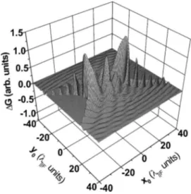
Figure6 shows a plot of the oscillatory part⌬G=Gop共0兲 −G0op of the conductance Gop共0兲, Eq.共62兲, as a function of the lateral position of the defect 0 for a fixed distance z0
from the interface. The oscillation pattern has a dead region in the center, corresponding to defect positions inside the classically inaccessible part of the metal for electrons in-jected by the point contact. This region is defined by the cone 共60兲and its radius00=z0/ cotcdepends on the depth of the
defect under surface. The oscillations in the conductance are largest when the defect is placed at the edge of the cone0
FIG. 5. Gray-scale plot of the modulus of the wave function in the planex= 0 for a warped cylindrical FS having the open direction along the contact axisz. The coordinates are measured in units of 储=ប/
冑
2m. The parameters used in the model are 1/= 0.9,b
冑
2m= 5.2, and a defect sits atr0=共0 , 13, 18兲.FIG. 6. Dependence of the oscillatory part⌬Gof the conduc-tance, as a function of the lateral position of the defect0 in the planez=z0. The open direction of the FS is oriented perpendicular
to the interface. The coordinates are measured in units of 储F =ប/
冑
2mF. The parameters used for the model FS共55兲are1/F= 0.9,b
冑
2mF= 6, and a defect sits at a depth ofz0= 11. In a central=00. In this case the defect is positioned in a direction of velocity belonging to the inflection line of the FS and the electron flux in this direction is maximal.
B. Direction of open FS parallel to the interface
The second orientation we want to discuss is that with the FS共55兲having its open direction共the axis兲parallel to inter-face, withp⬜=共px,pz兲andp储=py. The existence of a
classi-cally inaccessible region for this geometry leads to a strongly anisotropic current density in the xy plane. The expression for the point contact conductance without defect G0op be-comes
G0op=
e2R4共2−1兲2
4ប3b2U2 . 共68兲 The expressions for the phase, Eq. 共44兲, and the Gaussian curvature, Eq.共34兲, now read,
⌫0共
s兲共,
r兲= 1
ប
冉
冑共
x2+z2兲关2m共−1s兲兴+2兩y兩
b arcsin
冑
s冊
,共69兲 and
K0共s兲共,n兲=共− 1兲s1b
2sin4 4共−1s兲
冑冉
1 +2 cot 2
m1b2
冊
2
−8cot 2
m12b2 ,
共70兲 respectively. For this geometry we use spherical coordinates, with the angle between the vector r and the y axis. The variables1,2have been obtained from Eq.共31兲,
s=
1 2
冋
1 +2 cot2
m1b2 +共− 1兲
s
冑冉
1 +2 cot 2
m1b2
冊
2−8cot 2
m12b2
册
.共71兲 The first stationary phase point,1, corresponds to a positive Gaussian curvature and the second one, 2, to a negative curvature. For=c, Eq.共60兲, they become equal,
1=2= 1 2m1
共p⬜2max−
冑
p2⬜maxp⬜2min兲, 共72兲 and the curvature共70兲vanishes.Figure 7, acquired by using Eqs. 共37兲, 共69兲, and 共70兲, illustrates the interference of waves with different velocities the electrons emerging from the contact and the interference with the waves scattered by the defect.
Figure 8 shows a plot of the oscillatory part ⌬G of the conductance Gop共0兲 as a function of the lateral position of the defect0for a fixed distancez0from the interface. In this case two dead regions appear symmetrically with respect to the center of the oscillation pattern along the open direction of the FS. The center of the pattern corresponds to a defect sitting on the axis of the contact, 0= 0, for which 1= 0, 2= 1, sin= 1, and cos= 1. At this point Eq.共40兲takes the form
Gop共V兲=G0op
再
1 + 4gz022ប共p2⬜max+p⬜2min兲1b ⫻
冋
p⬜2minsin冉
2p⬜min共F+eV兲z0ប
冊
−p⬜2maxsin
冉
2p⬜max共F+eV兲z0ប
冊
+ 2p⬜maxp⬜min
⫻cos
冉
p⬜max共F+eV兲z0+p⬜min共F+eV兲z0ប
冊
册
冎
.共73兲
VII. DISCUSSION
We have analyzed the oscillatory voltage dependence of the conductance of a tunnel junction in the presence of an elastic scattering center located inside the bulk for metals with an anisotropic FS. These oscillations result from elec-tron waves being scattered by the defect and reflected back by the contact, interfering with electrons that are directly transmitted through the contact. The introduction of aniso-tropic electron movement beams the following implication: several points on the FS may share the same direction of the group velocity vectorvwhereas other directions forvcan be absent. Two nonspherical shapes for the FS have been inves-tigated: the ellipsoid and the corrugated cylinder共open sur-face兲.
Contrary to the case of a spherical FS 共Ref. 8兲 in the ellipsoidal model共46兲the center of the conductance oscilla-tion pattern does not need to coincide with the actual posi-tion of the defect but is displaced over a vector 00 =z0共mzz/mzx,mzz/mzy兲. When the STM tip is placed at this
point the oscillatory part of the conductance is given by FIG. 7. Gray-scale plot of the modulus of the wave function in the plane x= 0 for the warped cylindrical Fermi surface with the open direction along theyaxis and parallel to the plane of interface. The coordinates are measured in units of 储. The Fermi surface
parameters are 1/= 0.9, b
冑
2m= 5.2, and the defect position is r0=共0 , 10, 25兲. For this geometry the classically inaccessible region⌬G共V兲⬀sin
冉
2បz0
冑
2共F+eV兲mzz冊
. 共74兲The oscillation period depends on 1 /mzz, the component of
the tensor of inversive mass共35兲 for motion in thez direc-tion, and on the depth z0 of the defect. This allows us in principle to map out the positions of defects, as long as the shape of the FS is known. Apart from the period of the os-cillations, there is also information in the amplitude. Since short periods should correspond to small amplitudes this may be used for a test of consistency. However, quantitatively the amplitude is also influenced by unknown factors such as the defect scattering efficiency. The ellipsoidal FS is exceptional in that the problem can be solved exactly. This allows us to compare the calculation with the asymptotic approximation, and this shows that the approximation works very well for distances larger thanF.
In the case of the corrugated cylinder共55兲the open necks cause cones with opening angle 2c 共defined by the
inflec-tion line of the FS兲to be classically inaccessible. If the ori-entation is such that the open direction is orthogonal to the surface this will result in a dead region with radiusz0/ cotc
共60兲 where no conductance fluctuations can be observed. Thus, by measuring the size of this dead region we directly obtain the position of the defect. The oscillation amplitude will be maximal at the border of the dead region, since the current density will be highest in the direction of the group velocity at the inflection line. In analogy to a hurricane the “eye” is surrounded by a ring of intense currents. Such rings of high amplitude oscillations have already been reported very recently in experiments on Ag and Cu共111兲 surfaces.17
For our model FS, along this border the oscillating part of the conductance is, apart from a phase factor, described by
⌬G共V兲⬀sin
冉
4z0bប
冏
冉
冑
p⬜maxp⬜minp⬜max−p⬜min
+ arcsin
冑
p⬜max 2−p⬜maxp⬜min
2m1
冊
冏
=F+eV冊
, 共75兲 wherep⬜maxandp⬜minare the maximal and minimal radii of the surface of constant energy in the direction perpendicular to the axis of the cylinder共57兲,1is the amplitude of corru-gation of the FS, and 2/bis the size of the Brillouin zone. Again we find that the depth of the defect is determining the oscillation period, so that for given FS parameters this infor-mation can be exploited to investigate the structure of the metal below the surface.
If the open direction is parallel with the surface the high-est amplitude will be found with the STM tip straight above the defect. For 0= 0 the conductance oscillations are de-scribed by Eq.共73兲. Clearly, the oscillation pattern is more complicated than that from Eq.共74兲, since there are contri-butions from the belly as well as from the neck parts of the FS, plus a sum frequency. For small necks the signal will be dominated by the oscillation due to the belly.
Although the two models presented in this paper are still rather artificial, they provide insights that are quite valuable for experimental work in this field. The most prominent con-clusion is that the regular oscillations due to convex parts of the FS, that behave as for the isotropic FS discussed previously,8will often be dominated by signals due to special directions. On any surface that features regions of zero cur-vature, the strongest conductance fluctuations will come from electrons traveling with the group velocity of that re-gion. Not only does this hold for the inflection lines around the necks in the共111兲direction of, e.g., Cu, Ag or Au, it is also true for the almost flat facets in the共110兲direction of the same metals. In the case of an inflection line the signal will decay as r−5/3, whereas for a flat facet the signal does not decay at all. This effect can be exploited for imaging defects up to much larger depths than previously estimated. The par-ticular shape of the FS for nearly all metals contain many detailed features that will allow us to check the validity of the conclusions drawn from the measured data.17
ACKNOWLEDGMENTS
The authors thank M. Wenderoth for communicating his unpublished results. One of the authors 共Ye.S.A.兲 is sup-ported by a grant of the European INTAS Young Scientists program 共Grant No. 04-83-3750兲 and one of the authors 共Yu.A.K.兲was supported by the European Erasmus Mundus program on Nanoscience. This research was supported partly by the program “Nanosystems, nanomaterials, and nanotech-nology” of National Academy of Sciences of Ukraine. FIG. 8. Dependence of the oscillatory part⌬G of the
conduc-tance, as a function of the lateral position of the defect0 in the
1B. Ludoph, M. H. Devoret, D. Esteve, C. Urbina, and J. M. van
Ruitenbeek, Phys. Rev. Lett. 82, 1530共1999兲.
2C. Untiedt, G. R. Bollinger, S. Vieira, and N. Agraït, Phys. Rev. B
62, 9962共2000兲.
3B. Ludoph and J. M. van Ruitenbeek, Phys. Rev. B 61, 2273 共2000兲.
4A. Halbritter, Sz. Csonka, G. Mihály, O. I. Shklyarevskii, S.
Speller, and H. van Kempen, Phys. Rev. B 69, 121411共R兲
共2004兲.
5A. Namiranian, Yu. A. Kolesnichenko, and A. N. Omelyanchouk,
Phys. Rev. B 61, 16796共2000兲.
6Ye. S. Avotina and Yu. A. Kolesnichenko, Fiz. Nizk. Temp. 30,
209共2004兲 关J. Low Temp. Phys. 30, 153共2004兲兴.
7Ye. S. Avotina, A. Namiranian, and Yu. A. Kolesnichenko, Phys.
Rev. B 70, 075308共2004兲.
8Ye. S. Avotina, Yu. A. Kolesnichenko, A. N. Omelyanchouk, A. F.
Otte, and J. M. Van Ruitenbeek, Phys. Rev. B 71, 115430
共2005兲.
9I. M. Lifshits, M. Ya. Azbel’, and M. I. Kaganov,Electron Theory
of Metals共Consultants Bureau, New York,共1973兲.
10A. M. Kosevich, Fiz. Nizk. Temp. 11, 1106共1985兲 关Sov. J. Low
Temp. Phys. 11, 611共1985兲兴.
11V. V. Ustinov and D. Z. Khusainov, Phys. Status Solidi B 134,
313共1986兲.
12I. O. Kulik, Yu. N. Mitsai, and A. N. Omelyanchouk, Zh. Eksp.
Teor. Fiz. 63, 1051共1974兲.
13M. Ya. Azbel, Phys. Rev. B 43, 2435共1991兲.
14I. F. Itskovich and R. I. Shekhter, Fiz. Nizk. Temp. 11, 373 共1985兲 关Sov. J. Low Temp. Phys. 11, 202共1985兲兴.
15V. P. Maslov and M. V. Fedoriuk,Semi-classical Approximation
in Quantum Mechanics共D. Reidel, Dordrecht, 1981兲.
16G. Korn and T. Korn, Mathematical Handbook 共McGraw-Hill,
New York共1968兲.
17A. Weismann, M. Wenderoth, N. Quaas, and R. G. Ulbrich共