WCDM2 – Wafer-Level Charged Device Model
Testing with High Repeatability
Nathan Jack,
1Timothy J. Maloney,
2Bruce Chou,
2and Elyse Rosenbaum
1(1)
Department of Electrical and Computer Engineering
University of Illinois at Urbana-Champaign, 1308 W. Main St., Urbana, IL 61801
[email protected]
(2)
Intel Corporation
3601 Juliette Lane, Santa Clara, CA 95054 USA
Abstract—CDM-like unipolar pulses are generated at the wafer level with excellent repeatability and linearity. Pulse width and rise time resemble that of FICDM testers. In-situ pre- and post-stress curve tracing reveals the current failure threshold for the device under test.
I.
I
NTRODUCTIONSeveral test methods have been introduced for generating charged device model (CDM) stress at the wafer level [1]-[4]. Wafer-level testing is desirable for multiple reasons, including reliability assessment earlier in the design phase (before packaging), elimination of packaging cost, and elimination of unrealistic package parasitics when stressing small test structures.
Wafer-Level CDM (WCDM) [1] was designed to replicate the air discharge event of field-induced CDM (FICDM)—the package-level industry standard [5]. In WCDM, charge is stored on the capacitance formed between the grounded wafer and an overhead field plate; discharge occurs through the arc formed between the wafer and an approaching probe tip connected to the field plate. While this air discharge mechanism does resemble FICDM testing, the variability of the arc causes the peak current to vary by 30% or more from zap to zap. It was also observed that the arc caused the stressed pad to crater at moderate current levels and spray pad metal across the wafer. Moreover, the process of repetitively contacting the probe tip to the wafer for each discharge accelerates the dulling of the probe tip. Finally, the discharge current was measured through a band-limited transformer, the behavior of which had to be de-embedded from the measurement data to obtain the true time domain waveform [1][6].
Capacitively-coupled TLP (CC-TLP) [2][3] offers a more reproducible method for generating wafer-level CDM-like stress. During CC-TLP, a very fast TLP (VF-TLP) pulse is applied to the device under test (DUT) via a probe that contacts the wafer, with the return path formed by the capacitance CDUT between a large ground plane and the wafer over which it is suspended. Because the VF-TLP pulse is relay-actuated, repeatability can be very good. Displacement current during the pulse rising and falling edges generates a dual-polarity stress with each VF-TLP pulse. However, it is often desirable to
generate a single-polarity stress when debugging CDM failures or to avoid reverse-bias damage when testing standalone devices.
In this work, WCDM is modified to be relay-initiated for excellent repeatability. The single-polarity stress generated with the new system closely resembles FICDM waveforms and provides testing flexibility. The new system is named WCDM2 [7].
II.
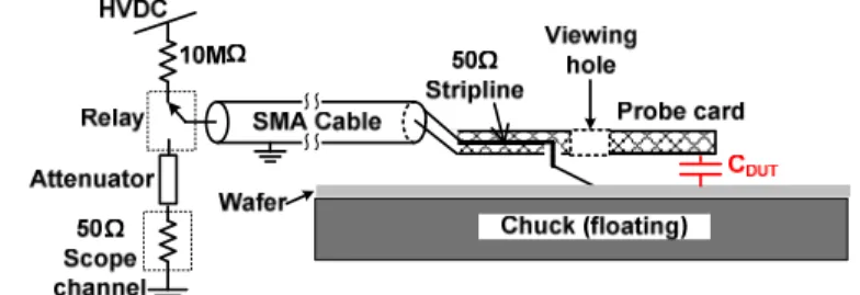
WCDM2
D
ESCRIPTIONA schematic of the WCDM2 tester is shown in Figure 1. The probe card is a three-layer PCB with field plates constructed on the outer two layers and a 50 Ω stripline trace in the center. The two field plates are shorted together and are connected to the center conductor of a SMA cable. The stripline connects the probe tip to the grounded shield of the SMA cable. A stripline was chosen over a microstrip design for its superior high frequency performance; microstrips suffer from multimodal, non-TEM (transverse electromagnetic) dispersion arising from the boundary discontinuity at the air-dielectric interface [8]. As shown in the photo in Figure 2, the probe card can be mounted to a micromanipulator for positioning. A hole in the center of the probe card allows the probe tip and wafer pads to be viewed through a microscope while positioning the tip. The probe tip lifetime is significantly improved over WCDM, since the tip may remain in contact with the wafer during multiple stresses. The probe tip used in this work has a radius of 10 μm, allowing for probing of small pads.
Figure 2: Photo of the WCDM2 probe card mounted onto A viewing hole in the center of the probe card allows the u when positioning the probe.
With the field plate at 0 V, the probe tip contact with the pad to be zapped; this brings the pad and the wafer to ground. Next, a merc connects the SMA cable to the high voltage D a 10 MΩ resistor, so that the cable, stripline, an capacitance CDUT are slowly precharged to the To initiate the stress, the mercury-wetted rel disconnect the high voltage supply and disch through the oscilloscope input channel. Attenu limit the voltage appearing at the scope i discharge of CDUT delivers a CDM-like stress t Non-air-discharge CDM has benefits fo testing as well. The WCDM2 charging mechanisms [7] are similar to that of the pac “CDM2” proposed by Given et al. [9].
III.
W
AVEFORMA
NALYSISA
NDC
A A calibration board was used to measu current stress felt by the DUT. The calibration a 1 ft by 1 ft square copper board with a 1 soldered into a hole in the center, as shown Figure 3. A SMA connector soldered to the disk resistor is connected through a cable to During a zap, the WCDM2 probe card is sus calibration board, and the probe needle makes center conductor of the disk resistor. The charg copper must travel through the disk resist grounded center during the zap. The oscillosco voltage across the resistor, from which the cu resistor can be extracted. All measurements work were taken using a 6 GHz oscilloscope.A.
Discharge Capacitance
Figure 4 shows the current waveforms zapping the calibration board with a 100 V increases with the area of the field plate on CDUT is a decreasing function of the separat field plate and the DUT. The measurements sh probe cards differing only in the length of the p
o a micromanipulator. use of the microscope
p is brought into s the potential of cury-wetted relay C source through nd plate-to-wafer e desired voltage. ay is actuated to harge the system uators are used to input. The rapid to the DUT.
or package-level and discharging ckage-level tester
ALIBRATION ure the WCDM2
board consists of 1 Ω disk resistor n in the photo in e backside of the an oscilloscope. spended over the s contact with the ge induced on the tor to reach the ope measures the urrent through the presented in this
measured while precharge. CDUT n the probe card;
tion between the hown are for two probe needle, i.e.
Figure 3: Photo of the calibration board. A 1 hole in the center of the 1 ft by 1 ft square soldered to the backside of the disk resisto oscilloscope. The oscilloscope measures the during a WCDM2 zap to the center conducto
the card with the longer probe need length of the longer probe tip was extract the capacitance, the total c zap was calculated by integrating time, as shown in Figure 5. Dividing V precharge voltage yields CDUT. T with the shorter needle was roughly 17 pF. The total charge for the othe a CDUT value of 12 pF.
Figure 4: Current measured when zapping a precharge voltage. Pulse width decreases wi CDUT is controlled by the probe tip length a
DUT.
Figure 5: Integrals of the current waveforms charge by the 100 V precharge voltage yields
-0.2
0
0.2
0.4
0.6
0.8
1
1.2
0
2
4
Cu
rre
n
t (A)
Time
0
0.2
0.4
0.6
0.8
1
1.2
1.4
1.6
1.8
0
5
Ch
arge
(n
C)
Time (ns)
1 Ω disk resistor is soldered into a copper board. A SMA connector or is connected by a cable to an resistor voltage, and thus current, r of the resistor.
dle has a smaller CDUT. The s approximately 2 mm. To harge injected during each the current waveform over g the total charge by the 100 The total charge for the card 1.7 nC, implying a CDUT of er card was 1.2 nC, yielding
a calibration board using a 100 V ith CDUT, as does the peak current.
nd the sizes of the field plate and
s from Figure 4. Dividing the total s the capacitance of each card.
4
6
8
e (ns)
17pF card
12 pF card
10
The pulse width and peak current both inc as seen in Figure 4. The pulse produced by discharge is approximately 1 ns wide with an at a precharge of 100 V; the 17 pF card p roughly 1.4 ns wide with a peak current of app at 100 V. These results may be understood WCDM2 waveform as the response of a RC n function with a non-zero fall time. Th schematically in Figure 6. The 1 Ω resisto calibration board disk resistor, and the capac CDUT, which is precharged to Vpre. The 56 Ω r the 50 Ω input of the oscilloscope plus an estim spark resistance in the mercury-wetted relay. C initiates the discharge of CDUT by complet ground. However, the ground loop is not established; there is a finite fall time associate tip inductance and the non-ideal transmission This fall time is captured by the finite step func
1 Ω
56 Ω
12 & 17 pF
Figure 6: RC model of the WCDM2 discharge path. The 1 the disk resistor on the calibration board, the 56 Ω resistor impedance plus spark resistance, and the capacitor repre zero fall time of the grounding signal represents the transmission line and relay.
The model in Figure 6 can be used to solve WCDM2 current i(t). This is can be accomplis Laplace domain. The step function can be ap decaying exponential with a fall time τf, which the Laplace domain as Vpre/(s + a), where a Kirchhoff’s Current Law to Figure 6 and resistances into a single resistor R, one obtains
Rearranging (1) and taking the inverse Laplac obtains
exp
exp
Increasing CDUT will proportionally inc charge stored for a given precharge voltage. primarily by the increase of the RC time discharge path, which appears in the second in (3). The result is a slower decay time an current pulse. Increasing CDUT also increases t
crease with CDUT, y the 12 pF card
amplitude of 1 A produces a pulse proximately 1.1 A
by modeling the network to a step his is illustrated or represents the citance represents
esistor represents mated 6 Ω for the Closing the relay ting the path to t instantaneously ed with the probe
n line and relay. ction in Figure 6.
1 Ω resistor represents r represents the scope sents CDUT. The
non-non-idealities of the
e for the transient shed easily in the pproximated as a h is represented in
= 1/τf. Applying d combining the s
. (1)
ce transform, one
(2)
. (3)
crease the total This is manifest
constant of the exponential term nd hence a wider the coefficient of
the exponential terms, resulting in current. Figure 7 shows the curren different values of CDUT, i.e. two cards, and Vpre = 100 V. The wave closely resemble the measured wave
Figure 7: Analytic solution of the WCDM2 values using (3) with Vpre = 100 V. The
closely resemble the measurements in Figure the 17 pF probe card results in a larger pul current.
B.
System Discharge Wavefor
The calibration board measur waveforms at the 1 Ω DUT (Figure measured at the scope input into w flows (see Figure 1) represents th WCDM2 system. This waveform i 100 V zap of the calibration board. the 50 Ω input impedance of the o the system discharge current. In represent the discharge of the SMA ns, a small spike is seen as the prob The last spike of the waveform, occ result of CDUT discharging.
Figure 8: Waveform measured by the scop discharge occurs. The first 9 ns of the curren Next, the stripline discharges. Finally, CDUT
ns point and onward.
0 0.2 0.4 0.6 0.8 1 1.2
0 2 4
Curre
nt (A
)
Time
n an increase in the peak nt predicted by (3) for two o different WCDM2 probe
forms obtained analytically eforms in Figure 4.
current for the two different CDUT
waveforms obtained analytically e 4. The larger RC time constant of
lse width and slightly higher peak
rm
rements show the current 4). However, the waveform which the discharge current he discharge of the entire is shown in Figure 8 for a
Dividing this waveform by oscilloscope channel yields Figure 8, the first 9 ns cable. Between 9 ns and 10 be card stripline discharges. curring at about 10 ns, is the
pe on the channel into which the nt represent the cable discharging. is discharged, occurring at the 10
4 6 8
e (ns)
The spikes in the system discharge wave impedance discontinuities along the disch impedances that are unequal to the 50 impedance of the SMA cable and oscillos reflection coefficient Γ at such points in the sys
Ω
+
Ω
−
=
Γ
50
50
L L
Z
Z
where ZL is the impedance looking into the sy of the impedance discontinuity. The spike discharge of CDUT is expected since the im capacitance is not 50 Ω [10]. However, th designed to have an impedance of 50 Ω, so it was unexpected.
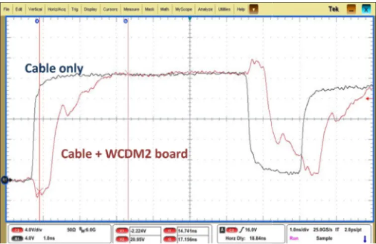
To extract the apparent impedance of the domain reflectometry (TDR) was used. T screenshot in Figure 9 compares the reflected w cable plus WCDM2 board to that of the cab cases the ends of the transmission lines wer The initial negative reflection seen on the wa WCDM2 board indicates that its impedance i Application of (4) yields ZL≈ 40 Ω.
Figure 9: Oscilloscope screenshot showing TDR response the cable connected to it, compared with the cable reflection at the WCDM2 board interface indicates a 40 Ω
contrary to the designed-for 50Ω impedance. The scales f div. on the vertical axis and 1 ns / div. on the horizontal ax
To understand why the stripline impedance important to note that the transmission line i cable-to-PCB interface. As illustrated in Figu conductor of the SMA cable is connected to th the stripline, while the SMA shield is connecte center conductor. The characteristic impedanc transmission line is given by
where L and C are the inductance and capa length, respectively. Conventionally, the ou stripline are at earth potential, so there is no the free-space capacitance from the outer nearby, grounded objects; C is therefore en
eform arise from harge path, i.e.
Ω characteristic scope input. The
stem is given by
(4)
ystem at the point arising from the mpedance of this he stripline was t causing a spike
e stripline, time-The oscilloscope
waveform for the ble only; in both re open-circuited. aveform from the s less than 50 Ω.
e of the WCDM2 plus alone. The negative
Ω stripline impedance, for this plot are 4 V / xis.
e is not 50 Ω, it is is inverted at the ure 8, the center he outer planes of ed to the stripline ce ZO of an ideal
(5)
acitance per unit uter planes of a charge stored on
planes to other ntirely contained
within the PCB. The stripline was equations derived under this a WCDM2, the outer planes of the st SMA center conductor and they a potential. C in (5) now comprises th plus the stray capacitance of the pl the nearby grounded shield of the Because C in (5) is larger than inten designed-for 50 Ω.
The stripline could be connected center to stripline center, SMA sh regain the designed-for 50 Ω impe Indeed, TDR measurements on the the conventional fashion reveal a c 50 Ω. In such a configuration, the p the wafer and the chuck on which it the potential on the high voltage increases CDUT by charging the str respect to ground. The result is a m constant and therefore a much wid undesirable for CDM-like testers.
If a 50 Ω stripline is desired, the designed to be smaller, i.e. the stri have an impedance greater th conventionally. Then, when connec depicted in Figure 8, the effecti reduced and the impedance would b the stray capacitance. However, t present system does not seem to cau the discharge path as indicated b discharge current measured by the c
C.
System Calibration
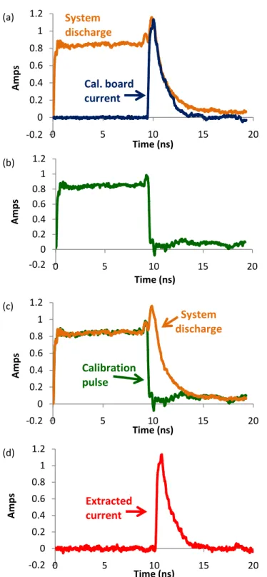
When zapping something other t calibration method is required to ex the system discharge waveform. Th Figure 10. First, the calibration bo discharge current are measured sim the desired precharge voltage. N current waveform is aligned suc coincident with the rising edge of discharge current waveform (Fig represents the discharge of CD Subtraction of the calibration boar discharge current measured yields (Figure 10b). For subsequent zap voltage, the calibration pulse can measured current (Figure 10c) to (Figure 10d). The calibration pu discharge and is independent of calibration pulse can be used to calc on-wafer DUT at the same precharg A calibration pulse is needed f that will be used during product te calibration measurements at each voltages to extract and store a calibr Or, a single calibration pulse can b
designed using impedance assumption. However, in tripline are connected to the
are charged to a non-zero he PCB stripline capacitance lanes to ground, such as to SMA cable (see Figure 2). nded, ZO is smaller than the
d conventionally (i.e. SMA hield to stripline shield) to edance signal transmission. same stripline connected in characteristic impedance of probe needle, and therefore t rests, would be charged to e supply. This effectively ray chuck capacitance with much longer discharge time der current pulse, which is
e PCB capacitance could be ipline could be designed to han 50 Ω if connected
cted in the inverted fashion ive capacitance would be be closer to 50 Ω because of the small mismatch in the use significant reflections to by the very sharp, narrow
alibration board (Figure 4).
than the calibration board, a xtract the DUT current from his method is illustrated in ard current and the system multaneously during a zap at Next, the calibration board
ch that its rising edge is the last peak in the system gure 10a); this last peak DUT as discussed earlier. rd current from the system
a calibration current pulse ps at the same precharge n be subtracted from the produce the DUT current ulse represents the system the DUT; therefore, the culate the current felt by any
e voltage.
Figure 10: (a) Current measured by the scope channel into which the system was discharged, compared with the current measured by the calibration board. (b) The calibration pulse calculated by subtracting the DUT current measured from the system discharge current. (c) On subsequent zaps, subtraction of the calibration waveform from the system discharge yields the DUT current. (d) The extracted DUT current from a subsequent zap.
use at multiple precharge voltages. The results are still quite accurate since the system response is essentially a linear function of the precharge voltage (see Figure 12). This is demonstrated in the following experiment. A calibration pulse was extracted for a 100 V precharge voltage; it was then used to calculate the DUT current during a subsequent 100 V
calibration board zap. As expected, the measured and calculated waveforms are nearly identical, as shown in Figure 11a. The 100 V calibration pulse current was then scaled up by a factor of 6 and was used to extract the DUT current from a 600 V zap. As shown in Figure 11b, the calculated and measured currents show close agreement, demonstrating that a single calibration pulse can be scaled and used at multiple precharge voltages with considerable accuracy.
The accuracy of the calculated calibration pulse will depend on proper alignment of the system discharge and calibration board waveforms (Figure 10a). Achieving good alignment is not difficult if a fast-sampling oscilloscope is used to acquire the waveforms; such a scope will provide several data points on the sharp rising edges for more precision in the alignment process. In any case, misalignment by several tens of picoseconds does not significantly alter the peak or the shape of the extracted DUT current.
The calibration procedure can be carried out entirely on an oscilloscope equipped with arithmetic capabilities. The system discharge and disk resistor waveforms can be simultaneously measured on separate channels then subtracted using built-in functions to produce the calibration pulse. The calibration pulse can be stored in memory, and on subsequent zaps it can be subtracted from subsequent system discharge waveforms to produce the DUT current instantaneously. A stored calibration pulse can also be appropriately scaled using built-in math functions and applied to subsequent measurements at multiple precharge voltages.
Figure 11: (a) A calibration pulse calculated for a 100 V precharge voltage was used to calculate the DUT current during a subsequent 100 V zap of the calibration board for a nearly identical match. (b) The 100 V calibration pulse was scaled by a factor of 6 and applied to a 600 V measurement; the calculated and measured currents show close agreement, demonstrating that a single calibration pulse can be scaled and used at multiple precharge voltages with considerable accuracy.
-0.2 0 0.2 0.4 0.6 0.8 1 1.2
0 5 10 15 20
Am
p
s
Time (ns)
(a)
System
discharge
Cal. board
current
-0.2 0 0.2 0.4 0.6 0.8 1 1.2
0 5 10 15 20
Am
p
s
Time (ns)
(b)
-0.2 0 0.2 0.4 0.6 0.8 1 1.2
0 5 10 15 20
Am
p
s
Time (ns)
System
discharge
Calibration
pulse
(c)-0.2 0 0.2 0.4 0.6 0.8 1 1.2
0 5 10 15 20
Am
p
s
Time (ns)
(d)
Extracted
current
100V
-0.2
0
0.2
0.4
0.6
0.8
1
1.2
0
2
4
6
8
Time (ns)
Amp
s
Calculated
current
Measured
current
(a)
600V
-2
0
2
4
6
8
0
2
4
6
8
Time (ns)
Am
p
s
Calculated
current
Measured
current
D.
Discharge Linearity and Repeatabil
The resistance of the spark generated discharge is a decreasing function of the precha consequence is that the FICDM peak curren function of the precharge voltage [9]. Du discharge, the spark is initiated in an controlled mercury-wetted relay, and the sp essentially independent of precharge voltage peak current is plotted as a function of prec Figure 12 for the case of a 17 pF card disc calibration board. The peak current is a linea precharge voltage, with roughly 1.2 A per 1 This linearity was verified from 100 V to 1000
Figure 12: WCDM2 peak current as a function of the prec 17pF probe card to zap the calibration board. Because the the controlled environment of the mercury-wetted relay, t constant, and the current increases linearly with voltage.
The repeatability of WCDM2 is signifi over WCDM and FICDM. Figure 13 shows a 50 repeated zaps of the calibration board at 10 variation is seen. In contrast, WCDM showe about 30% in the peak current at the same p [1]. The FICDM measurement tolerance is s [5], but this is often exceeded under various tes
Figure 13: Oscilloscope screen capture showing 50 con calibration board at 100 V. Variations are negligible. approximately 1 A, and the timescale is 2ns per major divi
IV.
COMPARISON WITH FIC
It is desirable that the current pulse genera is comparable to that of FICDM since it is0
2
4
6
8
10
12
0
200
400
600
8
Pe
ak
Cu
rre
n
t (A)
Precharge Voltage (V)
lity
during FICDM arge voltage. The nt is a nonlinear uring a WCDM2 environmentally-park resistance is
e. The WCDM2 charge voltage in charging into the ar function of the 100 V precharge. 0 V.
charge voltage using a e spark occurs within the spark resistance is
icantly improved screen capture of 00 V. Virtually no ed a variation of precharge voltage specified at 20% st conditions [9].
nsecutive zaps of the The peak current is ision.
CDM
ated by WCDM2 an industry-wide
standard [5]. A FICDM waveform are shown in Figure 14. The FICD while zapping the VSS pin of a lar with an effective discharge capac WCDM2 waveform is from a z structure on a full wafer with CDUT taken at a 500 V precharge voltage, been normalized to 1 A in Figure 14 and rise time are very similar to th 10%-90% rise time of the WCDM2 approximately 260 ps, while that o approximately 240 ps. The pulse approximately 1.08 ns, while for F 0.8 ns.
Figure 14: WCDM2 waveform from the zap full wafer compared to the FICDM waveform packaged Intel product. Both were taken a currents have been normalized to 1 A in both and rise time are very similar to FICDM puls
An even closer match of the WC FICDM could be achieved by mor time constant in the two system discharge path of a FICDM tester resistor plus an average spark resista is less than half the discharge resis includes the 50 Ω scope input WCDM2 card designed to have CD typical FICDM Ceff values should constant and therefore similar puls can range from a few pF for small large packages [11], so CDUT values in comparable WCDM2 pulse width
V.
DEVICE TESTI
An on-wafer standalone N+/Pwe WCDM2. The N+ terminal was gro was applied to the field plate, th charge on the substrate. Upon disch charge travels to the grounded N+ te junction. A semiconductor paramet to the chuck of the system and wa during the WCDM2 zap. Pre- and p obtained by forcing current from t terminal. As shown in Figure 15 occurred after a 6 A stress.00
1000
)
-0.2 0 0.2 0.4 0.6 0.8 1 1.2
0
Norma
liz
ed C
u
rrent
Time
and a WCDM2 waveform DM waveform was obtained rge, packaged Intel product citance Ceff of 16 pF. The zap to a standalone ESD
equal to 13 pF. Both were and the peak currents have 4. The WCDM2 pulse width hose of FICDM pulses. The 2 waveform in Figure 14 is of the FICDM waveform is width at the 50% point is FICDM it is approximately
of a standalone ESD structure on a m from the zap of a VSS pad on a at 500 V precharge, and the peak h cases. The WCDM2 pulse width es.
CDM2 pulse width to that of re closely matching the RC ms. The resistance in the
r consists of the 1 Ω disk ance of about 25 Ω [1]; this stance for WCDM2, which impedance. Therefore a DUT roughly equal to half of
produce a similar RC time se widths. The FICDM Ceff
packages to 10 - 20 pF for s of 5 – 10 pF should result hs.
ING RESULTS
ell diode was stressed using ounded, and a negative bias hereby inducing a positive harge, the positive substrate erminal, forward biasing the ter analyzer was connected as in high-impedance mode post-stress curve traces were the chuck to the grounded 5, damage to the junction
5
(ns)
Figure 15: (a) Forward-bias dc I-V curve of an on-wafer standalone N+/Pwell diode before (“Pre”) and after WCDM2 stress of increasing current levels. (b) DC current measured with a -1 V bias applied. Both plots indicate the device was damaged after a 6 A stress.
A dual-diode-protected receiver circuit with rail clamp was also stressed using WCDM2. Both the top and bottom diodes were sized similarly to the standalone N+/Pwell diode described above. The receiver input pad was grounded, and a positive potential was applied to the WCDM2 field plate, thereby storing negative charge on the substrate. Upon discharge, current flows from the input pad through the top diode and then through the rail clamp to ground. As seen in Figure 16, damage occurred after a 6A stress. It is concluded that the top diode was damaged because, in separate experiments, a standalone rail clamp passed 10 A of WCDM2 testing, and a similar receiver structure with diodes sized twice as large passed 10 A.
VI.
C
ONCLUSIONSWCDM2 produces repeatable current stresses that resemble those of FICDM testers, though with much better repeatability. Unlike FICDM, the peak current per precharge voltage is highly linear. WCDM2 allows for CDM-like stressing of products and smaller test structures without the need for packaging. The generated stress is unipolar – a benefit for debugging failure modes. A scalable calibration method was presented for calculating the current felt by the DUT. In-situ pre- and post-stress curve tracing may be performed to identify the current failure threshold.
A
CKNOWLEDGEMENTSThe authors thank A. K. M. Ahsan of Intel for the FICDM waveform.
Figure 16: (a) Forward-bias dc I-V curve of a dual-diode-protected receiver before (“Pre”) and after WCDM2 stress of increasing current levels. (b) DC reverse leakage current measured with a -1 V bias applied. The circuit was damaged after a 6 A stress. Experiments revealed that the top diode was the damaged device.
R
EFERENCES[1] B. Chou, T. Maloney, and T. Chen, “Wafer-level charged device model testing,” in Electrical Overstress/Electrostatic Discharge Symposium Proceedings, 2008, pp. 115-124.
[2] H. Wolf, H. Gieser, W. Stadler, and W. Wilkening,
“Capacitively coupled transmission line pulsing CC-TLP—A traceable and reproducible stress method in the CDM-domain,” in Electrical Overstress/Electrostatic Discharge Symposium Proceedings, 2003, pp. 338-345.
[3] H. Wolf, H. Gieser, and D. Walter, “Investigating the CDM
Susceptibility of IC’s at Package and Wafer Level by Capacitive Coupled TLP,” in Electrical Overstress/Electrostatic Discharge Symposium Proceedings, 2007, pp. 297-303.
[4] A. Gerdemann, E. Rosenbaum, and M. Stockinger, “A novel
testing approach for full-chip CDM characterization,” in Electrical Overstress/Electrostatic Discharge Symposium Proceedings, 2007, pp. 289-296.
[5] ESD Association, “Electrostatic Discharge Sensitivity Testing, Charged Device Model, Component Level,” Standard Test Method ANSI/ESD STM 5.3.1-1999, 1999.
[6] T. Maloney, “Evaluating TLP Transients and HBM
Waveforms,” in Electrical Overstress/Electrostatic Discharge Symposium Proceedings, 2009, pp. 143-151.
[7] T. Maloney, “TDT-CDM,” Presentation to CDM Standards
Committee, ESD Association Meeting, Anaheim, CA, Feb. 2009.
[8] H. Johnson. (2001, Apr.). Strange Microstrip Modes. EDN: Electronics Design, Strategy, News. [Online]. P. 32. Available:
http://www.edn.com/article/497702-Strange_microstrip_modes.php
0 0.001 0.002 0.003
0.5 0.6 0.7 0.8 0.9
Volts
Am
p
s
6.5A 6A 5.5A 5A Pre
(a)
0 1 2 3 4 5 6 7 8
-60 -40 -20 0
Current at -1V bias (microamps)
WC
D
M
2 cu
rr
e
n
t (
A
)
(b)
0 20 40 60 80 100
0 0.2 0.4 0.6
Volts
Mic
ro
am
p
s
6.5A 6A 5.5A 5A Pre
(a)
0 1 2 3 4 5 6 7
-30 -20 -10 0
Current at -1V bias (microamps)
W
C
D
M
2 cu
rr
e
n
t
(A
)
[9] R. Given, M. Hernandez, and T. Meuse, “CDM2 – A New CDM Test Method for Improved Test Repeatability and Reproducibility,” in Electrical Overstress/Electrostatic Discharge Symposium Proceedings, 2010, pp. 359-367.
[10] W. Dally and J. Poulton, Digital Systems Engineering.
Cambridge, United Kingdom: Cambridge University Press, 2001.