VSOP98260
www.vishay.com
Vishay Semiconductors
Preamplifier Circuit for IR Remote Control
MECHANICAL DATA
Pinning:
1, 4, 5= N.C., 2 = V
S, 3 = OUT, 6, 8 = GND, 7 = IN
FEATURES
• Carrier-out-function: carrier frequency and
burst length accurately correspond to the input
signal
• AC coupled response from 20 kHz to 60 kHz;
all data formats
• Small QFN package with 2 mm width
• Can be used with either a photodiode or an IR emitter in
forward or reverse polarity
• AC coupled input is insensitive to DC photocurrents
• Material categorization: for definitions of compliance
please see
www.vishay.com/doc?99912
ESD
• To maximize the sensitivity, the TIA input pin has minimal
ESD protection. Care should be taken never to touch or
otherwise expose this pin to an adverse ESD source. The
ESD protection conforms to Class 1B.
DESCRIPTION
The VSOP98260 is designed for use in an IR learning
application together with a photo PIN diode or IR LED as
optical detector. It is compatible with all data formats for IR
remote control. On the other hand it is immune to current
caused by light sources such as tungsten bulbs or
fluorescent lamps.
BLOCK DIAGRAM (simplified)
APPLICATION CIRCUIT
22906
PARTS TABLE
Carrier frequency 38 kHz VSOP98260
Package VSOP
Pinning 1, 4, 5 = N.C., 2 = VS, 3 = OUT, 6, 8 = GND, 7 = IN
Dimensions (mm) 2.0 W x 2.0 H x 0.76 D
Mounting SMD
Application Code learning
Pin 2
Pin 3
Pin 6, 8 Pin 7
TIA
30 kΩ
Signal shaping
Amplifier
BIAS
Recommended to minimize the connection distance between
VSOP98260
VS
Out In
Gnd
VS = 2.0 V to 3.6 V
IR LED Data
signal for emitter
Learning
mode
Microcontroller or logic to record the IR
VSOP98260
www.vishay.com
Vishay Semiconductors
Note
• Stresses beyond those listed under “Absolute Maximum Ratings” may cause permanent damage to the device. This is a stress rating only and functional operation of the device at these or any other conditions beyond those indicated in the operational sections of this specification is not implied. Exposure to absolute maximum rating conditions for extended periods may affect the device reliability.
Fig. 1 - Testsignal
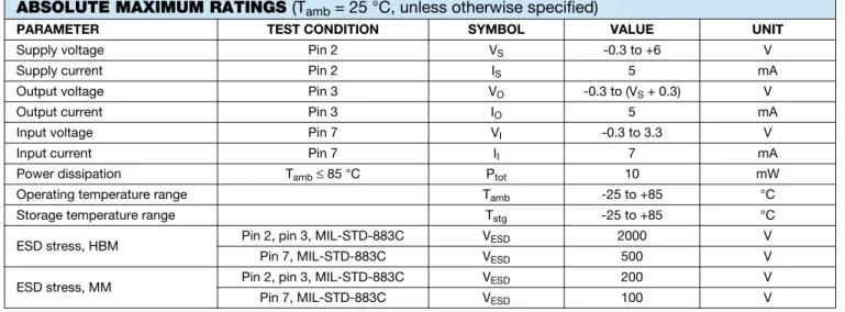
ABSOLUTE MAXIMUM RATINGS
(T
amb= 25 °C, unless otherwise specified)
PARAMETER TEST CONDITION SYMBOL VALUE UNIT
Supply voltage Pin 2 VS -0.3 to +6 V
Supply current Pin 2 IS 5 mA
Output voltage Pin 3 VO -0.3 to (VS + 0.3) V
Output current Pin 3 IO 5 mA
Input voltage Pin 7 VI -0.3 to 3.3 V
Input current Pin 7 II 7 mA
Power dissipation Tamb≤ 85 °C Ptot 10 mW
Operating temperature range Tamb -25 to +85 °C
Storage temperature range Tstg -25 to +85 °C
ESD stress, HBM Pin 2, pin 3, MIL-STD-883C VESD 2000 V
Pin 7, MIL-STD-883C VESD 500 V
ESD stress, MM Pin 2, pin 3, MIL-STD-883C VESD 200 V
Pin 7, MIL-STD-883C VESD 100 V
ELECTRICAL CHARACTERISTICS
(T
amb= 5 °C to + 85 °C, unless otherwise specified)
PARAMETER TEST CONDITION SYMBOL MIN. TYP. MAX. UNIT
Supply voltage VS 2.0 - 3.6 V
Supply current (pin 2) IIN = 0, VS = 5 V IS 0.55 0.7 0.9 mA
Output voltage low (pin 3) IOL = 2 mA VOL - - 100 mV
Output voltage high (pin 3) IOL = 0 VOH VS - 0.25 - - V
Internal pull up resistor
(pin 2, pin 3) RPU - 33 - kΩ
Max. input DC current VIN > 0 IIN-DCmax. 400 - - μA
Min. signal detection current IIN-DC = 0, fC = fBPF IIN-min. - 40 80 nA
IIN-DC = 100 μA, fC = fBPF IIN-min. - 50 - nA
Output accuracy
fC = 20 kHz to 60 kHz,
IIN = 80 nA to 50 μA,
testsignal see fig. 1, BER ≤ 2%
N carrier pulses
input burst length -1 cycle
input burst length
input burst length +1 cycle
counts
Carrier cycle
(26.3 μs in case of 38 kHz)
Delay time td
Photocurrent (input signal)
VSOP98260
www.vishay.com
Vishay Semiconductors
PACKAGE DIMENSIONS in millimeters
Proposed hole layout from component side (for reference only)
technical drawings according to DIN
specifications
Not indicated tolerances ± 0.1
Drawing-No.: 6.550-5314.04-4 Issue: -; 13.05.16
0.76 ± 0.05
0.2 ref.
2
2
0.5 typ. (6 x) (8 x) 0.25 ± 0.05
(8 x)
0.3 ± 0.1
0.2 min.
0.9 ± 0.15
1.6 ± 0.15
0.25 x 45°
10:1
0.35 (8 x)
(8 x) 0.65
1.3
0.5 (6 x) 1. Coplanarity (0.1 mm) applies to the exposed pad as well as the exposed terminals. 2. Package dimension does not
include mold flash, protrusions, burrs or metal smearing.
1 Pinning:
1. n.c. 2. VS
3. Out 4. n.c. 5. n.c. 6. GND 7. IN 8. GND
9826
YWW
Marking area
PIN 1 indicator
Chamfered corner PIN 1 indicator
Exposed pad
0.1
4
VSOP98260
www.vishay.com
Vishay Semiconductors
ASSEMBLY INSTRUCTIONS
Reflow Sol
d
ering
• Set the furnace temperatures for pre-heating and heating
in accordance with the reflow temperature profile as
shown in the diagram. Exercise extreme care to keep the
maximum temperature below 260 °C. The temperature
shown in the profile means the temperature at the device
surface. Since there is a temperature difference between
the component and the circuit board, it should be verified
that the temperature of the device is accurately being
measured
• Handling after reflow should be done only after the work
surface has been cooled off
Manual Sol
d
ering
• Use a soldering iron of 25 W or less. Adjust the
temperature of the soldering iron below 300 °C
• Finish soldering within 3 s
• Handle products only after the temperature has cooled
off.
VISHAY LEAD (PB)-FREE REFLOW SOLDER PROFILE
0 50 100 150 200 250 300
0 50 100 150 200 250 300
t (s)
T (°C)
255 °C
240 °C 245 °C
max. 260 °C
max. 120 s max. 100 s 217 °C
max. 20 s
max. Ramp Up 3 °C/s max. Ramp Down 6 °C/s
max. 2 cycles allowed
VSOP98260
www.vishay.com
Vishay Semiconductors
VSOP98260
www.vishay.com
Vishay Semiconductors
REEL DIMENSIONS in millimeters
LABEL
Stan
d
ar
d
bar co
d
e labels for finishe
d
goo
d
s
The standard bar code labels are product labels and used
for identification of goods. The finished goods are packed in
final packing area. The standard packing units are labeled
with standard bar code labels before transported as finished
goods to warehouses. The labels are on each packing unit
and contain Vishay Semiconductor GmbH specific data.
REELREEL SIZE (inch) REEL WIDTH (mm) TRAILER LENGTH (mm) LEADER LENGTH (mm) QANTITY PER REEL
7 8.4 160 400 3000
22610
Reel
Size
Reel Width
VISHAY SEMICONDUCTOR GMBH STANDARD BAR CODE PRODUCT LABEL
(finished goods)
PLAIN WRITTING ABBREVIATION LENGTH
Item-description - 18
Item-number INO 8
Selection-code SEL 3
LOT-/serial-number BATCH 10
Data-code COD 3 (YWW)
Plant-code PTC 2
Quantity QTY 8
Accepted by ACC
-Packed by PCK
-Mixed code indicator MIXED CODE
-Origin xxxxxxx+ Company logo
LONG BAR CODE TOP TYPE LENGTH
Item-number N 8
Plant-code N 2
Sequence-number X 3
Quantity N 8
Total length - 21