Abstract— For many digital communication system bandwidth and transmission power are limited resource and it is well known that the use of recursive convolution encoder (RCE) plays a fundamental role to increasing power and spectrum efficiency. The development of error correction technique with increasing coding gain has a limit, arising from the channel capacity. Convolution code is channel code, which extensively used in communication system.
The paper describes in three phases of Recursive convolution Encoder. System level design as first phase, containing trellis diagram and state table RTL vie of recursive convolution encoder also explains timing waveform and parameter require for developing the convolution encoder. Circuit level design using MOS transistor as second phase and then Layout or Physical design of recursive convolution encoder as third phase and finally explain the application and conclusion
I. INTRODUCTION
This paper is an introductory tutorial on, a new technique of error correction coding developed in the 1990s. The reader is expected to be familiar with the basic concepts of channel coding, although we briefly and informally review the most important terms. The paper starts with a short overview of channel coding and the reader is reminded the concept of convolution encoding. Shannon shows that the development of error correction technique with increasing coading gain has a limit, arising from the channel capacity. Convolutional codes are channel codes, which are extensively used in communication systems like GSM (global system for mobile communications) and Interim standard IS-95.We introduce a strategy to present convolutional codes without using mathematical structures. In this project, we will discuss our method to implement convolutional encoding and Viterbi Algorithm. It is unique design of Convolution Encoder in the all the three phases. The convolution encoder is a circuit that performs the convolution encoding scheme to encode data before transmission over a channel in digital communications system.
Pravin S. Tupkari
Department of Electronics & Telecommunication Sipna college of Engg. & Tech. Amravati, SGBAU Amravati University Amravati (MS) INDIA
Mobile No 9028372897 & 7588085957 Prof. A. S. Joshi
Department of Electronics & Telecommunication Sipna college of Engg. & Tech. Amravati, SGBAU Amravati University Amravati (MS) INDIA
II Channel Coding
The main aim of a digital communication system is to transmit information reliably over a channel. The available amount of transmitter power and bandwidth are the major constraints in the design of a digital communication system. The channel can be coaxial cables, microwave links, or fiber optic. The channel is subject to various types of noise, distortion, and interference. Also some communication systems have limitation on transmitter power. All these may lead to errors
Fig 1: Basic dig of convolution encoder
Consequently we may need some form of error control encoding to recover the information reliably. Convolution codes are extensively used for real time error correction. The position of the channel encoder is shown in above Fig 1, block diagram of the elements of a digital communication system
The task of channel coding is to encode the information sent over a communication channel in such a way that in the presence of channel noise, errors can be detected and/or corrected. We can explain here by recursive channel coding method:
Recursive Convolution Encoder.
Requires only error detection: if an error is detected, the sender is requested to retransmit the message. While this method is simple and sets lower requirements on the code’s error-correcting. The following fig 2. shows block dig of backward error correction and their state dig.
―FRONT END TO BACK END VLSI DESIGN
FOR RECURSIVE CONVOLUTION
ENCODER‖
International Journal of Advanced Research in Computer Science and Electronics Engineering (IJARCSEE) Volume 1, Issue 9, November 2012
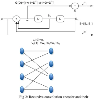
Fig 2: Recursive convolution encoder and their state diagram
The above figure shows that the block dig of the back word error correction with the state diagram. Form the state diagram the state Table 1 is shown in below. The state Table shows the output of encoder depends on present state and next state.
INPUT U
PRESENT STATE(S1,S0)
NEXT STATE (S1,S0)
OUTPUT (V1,V2)
0 00 00 00
1 00 10 11
0 01 10 00
1 01 00 11
0 10 11 01
1 10 01 10
0 11 01 01
1 11 11 10
Table 1: State table of recursive Convolution Encoder
The encoding sequence 0110 to the backward error correction and then output sequence is 00 11 01 01 it shown by the dark green line in trellis dig.
: Fig 3: Trellis diagram of Recursive convolution encoder
The above Fig 3 shows the trellis diagram of backward error correction it has the state 00, 01.10 and 11 as the encoder is in present state and the switch to next state then the output has been change suppose the encoder has present state is 00 and it is switch to the next state has a clock signal is 0 the output is 00 and it is represented as 0/00. Similarly the output is same state but the clock signal is 1 then output is 11 and it is represented as 1/11. In this way all the state are shows in the trellis diagram.
Since project has three phases System level, Circuit level, and Transistor level design (chip layout).
3.1System Level Design
In the first phase of system level design of recursive forward convolution encoder Quartus II i.e Qsys system integration tool is used to create design with fast and easy system-level integration. In this we seen the RTL view and the Timing diagram of convolution encoder and analyses the Total logic element, combinational function and dedicated logic resister used in both the cases. Also we have to shows Total Thermal power dissipation, core dynamic Thermal power dissipation and I/O Thermal power dissipation For the Recursive convolution encoder
The RTL View and Technology Map Viewer provide a hierarchy list that displays a representation of the project hierarchy and a schematic view that displays the components of the design element we want to examine. The hierarchy list expands as you navigate through the schematic view. we can also open the implementation of a design instance by double-clicking an instance in the hierarchy list.
In the schematic view, different default colors are used to discern different design elements. For example: All encrypted design and I/O pins instances appear gray.
All state machine nodes appear yellow (RTL Viewer only).
All logic cells and I/O cells for which you can view the underlying internal implementation appear blue (Technology Map Viewer only).
All RAM blocks and DSP blocks appear blue.
All other design instances appear light green.
Fig 4: Recursive Convolution encoder with RTL view
Fig 5: Recursive Convolution encoder timing waveform
The above Fig 5 shows the timing diagram of RCE. The output Q1, Q0 and ffout is depend upon the clk, rst and the data d which is shown on the above fig. 5 The output Q1, Q0 and FFout is depend upon the clk, rst and the i/p data d (101101) which is shown on the above figure and the respective timing wave form of qois110001 and the output q1 is 100110 where the Reset signal is initiated at falling edge of the first clock signal.
Fig 6:Parameter 1 of recursive Convolution encoder
The above Fig 6 shows the parameter used in the RCE in which Total logic element is 1outof 14448 , total combinational function 2/14448 and the dedicated logic register is 3/14448, total pins is 3, total memory bit used used is 0 and other parameter is shown in above table.
Fig 7: Parameter 2 of recursive Convolution encoder
Fig 7 shows the parameter used i.e. Total Thermal power dissipation, core dynamic Thermal power dissipation and i/o Thermal power dissipation. for the Recursive convolution Encoder(RCE).
3.2 Circuit Level Design
circuit schematic design Recursive convolution encoder was not too complicated as it involves a three Flip-Flop, three EX-OR gate, and voltages sources and their connections all of which we were familiar with their workings and their implementation using MOSFETs. Fig 8 shows schematic block of recursive convolution encoder
Fig8: Schematic Recursive Convolution Encoder
The above figure shows the circuit level design (using MOS Transistor). It consists of three FF acts as shift resister combine with the EX-OR gate and the output Q1, Q2 shows at the EX-OR o/p. The following Fig 9 shows the relevant timing waveform of circuit level design of RCE. This timing waveform is same as that of convolution encoder at system level design
Fig 9: Simulated o/p of Recursive convolution encoder
The relevant waveform of circuit level design of Recursive Convolution Encoder. The output Q1, Q0 and FFout is depend upon the clk, rst and the i/p data d (101101 ) which is shown on the above figure and the respective timing wave form of q1 is 100110 where the Reset signal is initiated at falling edge of the first clock signal. From above discussion it is clear that the timing waveform obtained at circuit level design and system level design are same (i.e. in both cases the output q1 is 100110) and hence it clear that the design at both the level is true for same data input for (RCE).
3.3 Transistor Level Design
International Journal of Advanced Research in Computer Science and Electronics Engineering (IJARCSEE) Volume 1, Issue 9, November 2012
and optimized for minimal area use in coordination with the desired W/L for the final layout of our chip.
Once the dimensions for each block (XORs, T-Gate, flip-flops) were optimized, we laid them in a higher level cell which included the outline of the maximum size and the six contact pads. We then completed the interconnections, making minor alterations to lower-level cells when necessary.
It should be noted that our submitted layout had the dimensions 221 λ x 222 λ, a subtle, but all the same, a reduction in size compared to the allowed dimensions of 230 λ x 230 λ. This means that our chip has the physical dimensions of 552.5μm x 555μm.
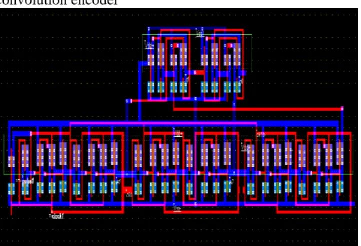
The following fig 10 shows the layout of recursive convolution encoder
Fig 10: Layout of Recursive Convolution Encoder
Chip Layout Discussion
Most of the transistors in our layout were of minimal, but properly ratioed, sizes. This design decision was made solely because of area constraints. Our functional blocks occupy a significant amount of space on the chip and, as well, so do interconnects. This decision was rationalized by the fact that we would only be driving a 10pF load and operating this chip at fairly low frequencies (few MHz) and in optimal operating conditions (room temperature).
Fig11: Wave form of transistor level design
The minimal gate widths make for a slower pull of current, but this was acceptable for our purposes, as long as we ratio our transistors correctly.
The above Fig 11 shows the relevant waveform of Transistor Level design of Recursive Convolution Encoder. The output Q1, Q0 and FFout is depend upon the clk, rst and the i/p data d (101101 ) which is shown on the above figure indicated by green line and the respective timing wave form of q1 is 100110 indicated by dark green line where the Reset signal is initiated at falling edge of the first clock signal. From above discussion it is clear that, design at System level, Circuit level and the Transistor level match because the timing waveform at three stage are same or equal (i.e. input data101101 is applied at all the three phases of design and the output at q1 is 100110 at all the three phases all the circuit design at three stages is match for same data). Hence our aims is true.
4.0 Conclusion:
The contribution of this paper is to provide a simulating tool that teaches efficiently the convolution encoding in digital communication, and wireless communication courses. In this paper we have work on three phases of VLSI Design 1). System Level Design [VHDL coding] 2).Circuit level design using MOS Transistor. 3). Layout or Physical level design and we have found that all three level the relevant waveform are same in recursive convolution encoder. Hence our aims is true.
5.0 Application:
Convolution code are extensively used in numerous application in order to achieve reliable data transfer , including digital video, radio, mobile communication, and satellite communication with hard decision code
1) A satellite modem or sat modem is a modem used to establish data transfer using a communication satellite as a relay. There is a wide range of satellite modems from cheap device for home internet access to expensive multifunction equipment for enterprise use. A satellite modems main function is to transfer input bit stream to radio signal to vice-versa
2) A Viterbi decoder uses the Viterbi algorithm for decoding bit stream that has been encoded using Forward error correction based on convolution code. The viterbi decoding algorithm is widely used in the following area
Decoding trellis coded modulation (TCM), the technique used in telephone –line modems to squeeze high spectral efficiency out of 3 khz bandwidth analog telephone lines. The TCM is also used in the PSK31digital mode for amateur ratio and sometime in the radio relay and satellite communication
3) Another concern of coding theory is designing codes that help synchronization. A code may be designed so that a phase shift can be easily detected and corrected and that multiple signals can be sent on the same channel
demodulation process is performed to recover the data. The properties of this class of codes allow many users (with different codes) to use the same radio channel at the same time. To the receiver, the signals of other users will appear to the demodulator only as a low-level noise.
5) Another general class of codes are the automatic repeat request (ARQ) codes. In these codes the sender adds redundancy to each message for error checking, usually by adding check bits. If the check bits are not consistent with the rest of the message when it arrives, the receiver will ask the sender to retransmit the message. All but the simplest wide area network protocols use ARQ. Common protocols include SLDC (IBM), TCP (Internet), X.25 (International).
6.0 References
[1] C. E. Shannon, ―A mathematical theory of communications—Part I,‖Bell Syst. Tech. J., vol. 27, pp. 379–423, 1948.
[2] D. Divsalar and F. Pollara, ―Hybrid concatenated codes and iterative decoding,‖ in Proc. ISIT’97, Ulm, Germany,July 1997. [3] S. Benedetto, D. Divsalar, G. Montorsi, and F. Pollara, ―Soft-outpu
tdecoding algorithms for continuous decoding of parallel concatenated convolutional codes,‖ in Proc. ICC’96, Dallas, TX, June 1996.
[4] A. J. Viterbi, ―An intuitive justification of the MAP decoder for convolutional codes,‖ IEEE J. Select. Areas Commun., vol. 16, pp. 260–264, Feb. 1998.
[5] L. C. Perez, J. Seghers, and D. J. Costello, ―A distance spectrum interpretation of turbo codes,‖ IEEE Trans. Inform. Theory, vol. 42, pp. 1698–1709, Nov. 1996.
[6] S.A. Barbulescu and S.S. Pietrobon. Turbo codes: A tutorial on a new class of powerful error correction coding schemes. Part II: Decoder design and performance .J. Elec. and Electron. Eng., Australia, 19:143–152, September 1999.
[7] University of South Australia, Institute for Telecommunications Research, Turbo coding research
[8] Third Generation Partnership Project(3GPP). Multiplexing and Channel Coding(FDD), March 2005. TS 25.212 Version 6.4.0. [9] F. MacWilliams and N. Sloane, The theory of error–correcting