2210 IEEE TRANSACTIONS ON ELECTRON DEVICES, VOL. 46, NO. 11, NOVEMBER 1999
Design and Analysis of High-Speed
Random Access Memory with Coulomb
Blockade Charge Confinement
Kozo Katayama, Hiroshi Mizuta,
Member, IEEE, Heinz-Olaf M¨uller,
David Williams,
Member, IEEE, and Kazuo Nakazato
Abstract— A silicon-based memory cell utilizing Coulomb blockade is analyzed for use as a high-speed RAM. Operation principles and design guidelines are given by simple analytical modeling and simulations. By performing transient waveform Monte Carlo simulations, high-speed write operation is demonstrated with a time shorter than 10 ns. The memory node voltage of less than 0.1 V is detected by a newly proposed split-gate cell structure with a minimum disturbance to/from nonselected cells, which indicates the compatibility of this structure with conventional field effect transistors.
Index Terms— Cell design, Coulomb blockade, high-speed RAM, simulation, single electron.
I. INTRODUCTION
P
RESENT memory architectures such as the dynamic random access memory (DRAM) are now approaching fundamental difficulties. One of the inherent problems in DRAM is the amount of charge stored in cell capacitors. The amount of stored charge must be maintained to ensure noise margins sufficient for sense amplifiers to detect the signal. This is a serious restriction on the further scaling down of DRAM cell sizes. Therefore, the gain cell structure realized in FLASH memories is a candidate to remedy the situation, along with the development of high dielectric capacitor materials. Nanocrystal memories proposed recently [1], [2] have a poten-tial to realize small memory cells, where stored charge might be scaled down to a single electron. However, in these cells, charge is injected into floating nanocrystals through potential barriers such as gate oxides by standard (Fowler–Nordheim) tunneling processes, as in FLASH memories. Consequently, the write speed is rather slow in these memories compared to the present DRAM. In this paper we propose a new memory cell architecture called lateral single electron memory (L-SEM) which enables high-speed write operation comparable to DRAM. In this scheme, a tunnel junction array with small junction capacitances and relatively low tunnel resistances isManuscript received July 23, 1998; revised April 22, 1999. This work was performed within the ESPRIT MEL-ARI project FASEM (Fabrication and Architecture of Single-Electron Memories). The review of this paper was arranged by Editor D. P. Verret.
K. Katayama was with Hitachi Cambridge Laboratory, Hitachi Europe Ltd., Cambridge CB3 0HE, U.K. He is now with Central Research Laboratory, Hitachi Ltd., Kokubunji, Tokyo 185, Japan.
H. Mizuta, H.-O. M¨uller, D. Williams, and K. Nakazato are with Hitachi Cambridge Laboratory, Hitachi Europe Ltd., Cambridge CB3 0HE, U.K.
[image:1.612.321.545.208.482.2]Publisher Item Identifier S 0018-9383(99)07210-X.
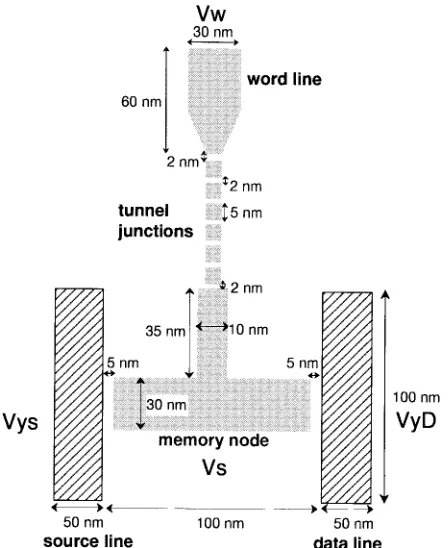
Fig. 1. L-SEM structure with a one-dimensional tunnel junction array and a memory node which acts as the gate of the sense MOSFET.
used to inject and remove the charge stored in the mem-ory node, instead of the tunnel oxide used in FLASH-type nanocrystal memories.
II. DESIGN ANDOPERATION PRINCIPLES
In this paper, we consider the memory cell structure shown in Fig. 1, which is based on the recent experimental work [3]. An in-plane tunnel junction array [4] is integrated into the gate of a MOSFET, and the write operation is achieved by electrons tunneling through the junctions between the word electrode and the memory node. The stored data is maintained by the Coulomb blockade of the tunnel junctions and is sensed by applying a small voltage between the source and the drain electrode. The single electron switching operation of the tunnel junctions is not used in this scheme. As a result, the background charge effects which are serious in single-electron transistor operations are greatly alleviated [5]. An array of
(a)
(b)
[image:2.612.133.475.53.434.2](c)
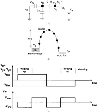
Fig. 2. (a) Simplified equivalent circuit for analytical modeling of the memory cell, (b) potential barrier due to Coulomb blockade, and (c) applied voltages in write operation and standby states.
tunnel junctions is effective in obtaining a higher Coulomb gap as well as in averaging out the background charge fluctuations. The Coulomb gap of an infinitely long, uniform array is given as [6]
(1)
where and are tunnel junction and stray capacitances and is an elementary charge. The number of junctions should
be about because approaches the value of (1) at
the junction length The Coulomb gap of disordered arrays due to the effect of background charge and other effects is discussed in [5], [7], and [8].
A. Write Operation
To analyze the operation of the memory, a simplified equivalent circuit described in Fig. 2(a) is considered. Since the free energy of the system has a maximum value, as shown in Fig. 2(b), when the charge is placed at one of central islands, only this island is taken into account. We assume as the total serial capacitance between the island and the memory node and as that between the island and the word line.
is the memory node capacitance which is realized by the gate of a MOSFET. The write operation sequence is described in
Fig. 2(c). To write “0”, positive is applied
to the common source and data line of the selected column of the array to shift the memory node voltage, and at the same time, a negative word line voltage is applied to a selected row. In this way, a cell is selected out of the entire array. To write “1”, the opposite polarity voltages are applied to the data and word line, which brings the “0” state outside the blockade region and causes a transition. The memory node voltage when and are applied is given as
(2)
If the memory node is charged until
is satisfied. Combined with (2), the word line voltage and data line voltage required to charge the memory node to is obtained as
2212 IEEE TRANSACTIONS ON ELECTRON DEVICES, VOL. 46, NO. 11, NOVEMBER 1999
has to be satisfied to keep the data at the standby condition when and are kept at zero. To avoid data destruction in nonselected cells to which one of and is applied during write cycles, the following conditions are required:
(4)
(5)
When the write voltages are sufficiently high, the time required to charge up the memory node is simply given by the time constant of the system
(6)
where is the total resistance of serial tunnel junctions.
B. Retention Time
The retention time of the memory can be evaluated based on the orthodox theory of single electron tunneling [9]. The electrostatic energy of the system as a function of the memory node charge , the island charge , and the word line voltage is calculated based on the thermodynamics of electrostatic systems
(7)
Solving charge conservation relations
we obtain and as
where we assumed is fixed at zero and is included in Integrating (7) and calculating the difference between the final and the initial states of a single charge tunneling event, the barrier height is given as
(8)
where the Coulomb gap is
(9)
When , (9) is reduced to
which is independent of Thus, a memory cell with a large node capacitance does not deteriorate the Coulomb blockade characteristics.
The tunneling rate is expressed according to the orthodox theory of single electron tunneling as
(10)
We define the retention time of the memory as the half life time of the initial stored charge , namely,
Solving , we obtain
Hence
(11)
When , substituting
which maximizes (11), we finally obtain a simple formula for the retention time as a function of
(12)
III. SIMULATION OF WRITE ANDREADOPERATION
A. Write Operation
To estimate the possible write-speed performance of the L-SEM, the structure shown in Fig. 1 was investigated in-cluding all the coupling constants between small islands and electrodes on a silicon substrate. Design parameters were cho-sen within the possible reach of precho-sent-day silicon nanowire formation technologies [10]. Detailed capacitance parameters between every conductor on the plane were determined by a two-dimensional (2-D) capacitance simulator, with which all the self- and cross-capacitances between the conductors are calculated under the assumption of negligible conductor thicknesses. Full memory write sequences were then simulated using a single-electron Monte Carlo simulator [5], [11] based on the orthodox theory of single electron tunneling without cotunneling effects. The simulation was done for a temperature of 4.2 K for a 5-nm-island memory cell with tunnel junction resistances of 1 M , which is sufficiently larger than the
quantum resistance If the full capacitance
parameters are reduced to conform with the simplified circuit discussed in the previous section, memory node capacitance
is 32 aF, aF, aF, and aF
(a)
[image:4.612.111.492.61.480.2](b) (c)
Fig. 3. (a) Simulated Coulomb blockade characteristics of a 1-D tunnel junction array with six 52 5 nm2islands in the geometry shown in Fig. 1. A Coulomb gap of 0.1 V is realized with this size of island. (b), (c) The hysteresis loop of the memory node voltage as a function of common source and data voltageVD, obtained by a Monte Carlo simulation when the write sequence cycle in Fig. 2(c) withVww= 180 mV and VDw= 100 mV was executed. The
upper and lower branches of the hysteresis correspond to+35e (the absence of 35 electrons) and 035e (the presence of 35 electrons) charge states, respectively.
(1), and mV and mV are required
to write the data.
Fig. 3(a) shows the Coulomb blockade characteristics of the tunnel junction array obtained by a Monte Carlo simulation. Based on this obtained value of and the conditions (3),
(4), and (5) and were chosen to be 100 and 180
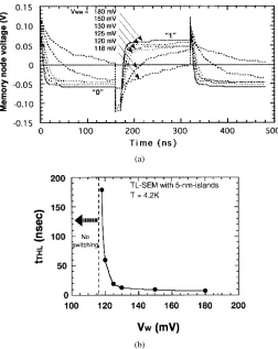
mV, respectively, and the write sequence operation was sim-ulated. Fig. 3(b) shows the simulated node voltage hysteresis characteristics when the voltage sequence shown in Fig. 3(c) is applied. The upper branch of hysteresis corresponds to the state “1” where 35e charges are stored at the memory node and the lower branch to the state “0” with 35e charges. The temporal evolution of the memory node voltage during write cycles is shown in Fig. 4(a) for various word line voltages. The rise and fall time of the curves depends strongly on the word line voltage. The switching becomes faster with increasing since a larger results in a larger tunneling current
through the tunnel junctions, leading to faster charging-up. In Fig. 4(b), the switching time is plotted as a function of
, where is defined as the time of the curve.
The switching occurs at a threshold voltage determined by (3)
with and then decreases rapidly. It can be seen
that can be reduced to less than 10 ns for the present cell structure.
B. Read Operation
2214 IEEE TRANSACTIONS ON ELECTRON DEVICES, VOL. 46, NO. 11, NOVEMBER 1999
(a)
[image:5.612.42.294.56.373.2](b)
Fig. 4. (a) Transient memory node voltage simulated with various values of
Vww for the L-SEM with 52 5-nm2-island tunnel junctions at 4.2 K. (b)
Vwwdependence of rise/fall timetT HL: Fast switching is achieved between high and low levels with a switching time as short as 10 ns.
nondestructively in a selected cell in an array, because the Coulomb blockade voltage is low. The second problem is how to realize a small memory node size compatible with the small scale of tunnel junctions, because conventional MOSFET’s have scaling limitations due to short channel effects. In order to reduce the memory node size, we propose a cell selection scheme shown in an equivalent cell array circuit [Fig. 5(a)], where a selected memory node is connected to the data line through MOSFET’s driven by a separate read word line. A realistic cell layout for this structure is shown in Fig. 5(b). A diffusion layer is used for the source and data line to reduce the number of metal layers. The gate of the MOSFET is divided into three parts, the middle one of which is the memory node. The other two parts of the gate act as switch transistors to connect the memory node MOSFET to the data line. The threshold voltage of the memory node MOSFET is set between the charge states of “0” and “1”. The size of the memory node can thus be made smaller than without the side gates (Fig. 1), because the short channel effect is relaxed by them. However, it should be noted that the smaller the node size is, the higher Coulomb gap is still required because is raised higher by the capacitive coupling with the read word line during read operations. The required Coulomb gap for nondestructive
reading is given as , where
is the capacitance between the side gates and the memory node.
(a)
[image:5.612.319.552.59.433.2](b)
Fig. 5. (a) Equivalent circuit of a cell array for the split-gate memory node scheme. (b) A layout of the cell structure with split-gate MOSFET’s. The original gate (length:L1) is divided into three parts. The memory node gate (length:L2) is separated from the two side gates with a spacing ofLs:
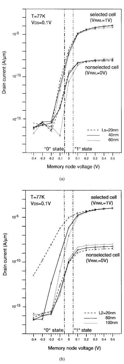
The characteristics of this sense MOSFET were investigated by using a 2-D device simulator with the conventional drift-diffusion model. Simulated drain current characteristics of read MOSFET’s for the split-gate structure are shown in
Fig. 6. We assumed V is applied to a selected
word line, whereas a nonselected word line is kept at zero. Sufficient current modulation can be obtained by changing the memory node voltage. The drain current can flow as much as 1 A/ m for a 50 mV node voltage. If we assume a 0.1 0.1 m memory node size, about ten electrons are stored at the voltage. The change of the memory node voltage between 50 and 50 mV modulates the drain current by three orders of magnitude and the current difference between the selected and nonselected cell also amounts to three orders of magnitude. These signals will be sufficient to be amplified by standard MOS sense amplifiers even for a realistic large array size with 128 128 cells.
(a)
[image:6.612.63.274.46.662.2](b)
Fig. 6. (a) Dependence of theI0V characteristics of sense MOSFET’s on the gap lengthLsof the split-gate.Lswas changed between 20 and 60 nm. The memory node gate lengthL2was kept at 0.1m. (b) Dependence of the
I0V characteristics of sense MOSFET’s on the memory node size L2: Ls
was kept at 40 nm. Other relevant parameters in the simulation are: side gate length 0.36m, gate oxide thickness 10 nm, drain voltage 0.1 V, temperature 77 K. The doping profile of the MOSFET’s was chosen so that the threshold voltage became 0 V, namely, n-type doping of 5 2 1016 cm03 at the surface with the p-type substrate of 22 1016 cm03:
channel effect because no doping profile optimization is done in this simulation. When a 20 20 nm memory node is realized, the stored charge in the memory node would be reduced to a few electrons.
IV. DISCUSSION
Our analyses carried out so far suggest that a write speed comparable with the present DRAM is achieved, with the possibility of combining a Coulomb blockade memory with conventional MOS transistors to read the data. The largest problem left to be investigated is the retention time. Assuming
M K, and V, the
formula (12) gives ns, although at K
the lifetime is almost infinite. To obtain a retention time of 1 s comparable with DRAM’s, a Coulomb gap of 0.36 V is
required at K and 1.5 V at K. This means that
rather high voltage operation is required for such an atomic scale device.
From the cell layout point of view, a lot of optimization of the structure is required. The lateral structure proposed here has the apparent demerit of a large cell size. At present, there is no well-developed silicon-based technology to fabricate vertical tunnel junction layers with sufficiently small dimen-sions enough to exhibit the charging effect. A vertical tunnel junction fabricated, for example, by nitridation of silicon [12] might be available in realistic implementations.
In conclusion, we have shown design guidelines for a ran-dom access memory cell where data is maintained by Coulomb blockade, and which is compatible with conventional MOS transistors. With relatively low tunnel resistance junctions for which cotunneling can still be neglected, faster operation than present day DRAM is possible. However, compatibility between faster operation and longer retention time at a room temperature still remains to be solved.
ACKNOWLEDGMENT
The authors would like to thank Dr. K. Ito for stimulat-ing discussion about the problems of conventional memories and S. Biesemans for critical comments on the L-SEM cell structure and operation.
REFERENCES
[1] K. Yano, T. Ishii, T. Hashimoto, T. Kobayashi, F. Murai, and K. Seki, “Room-temperature single-electron memory,” IEEE Trans. Electron De-vices, vol. 41, pp. 1628–1638, 1994.
[2] S. Tiwari, F. Rana, H. Hanafi, A. Hartstein, and E. F. Crabe´e, “A silicon nanocrystals based memory,” Appl. Phys. Lett., vol. 68, pp. 1377–1379, 1996.
[3] Z. A. K. Durrani, A. C. Irvine, H. Ahmed, and K. Nakazato, “A mem-ory cell with single-electron and metal-oxide-semiconductor transistor integration,” Appl. Phys. Lett., vol. 74, pp. 1293–1295, 1999. [4] K. Nakazato, R. Blaikie, and H. Ahmed, “Single-electron memory,” J.
Appl. Phys., vol. 75, pp. 5123–5134, 1994.
[5] H.-O. M¨uller, K. Katayama, and H. Mizuta, “Effects of disorder on the blockade voltage of two-dimensional quantum dot arrays,” J. Appl. Phys., vol. 84, pp. 5603–5609, 1998.
[6] N. S. Bakhvalov, G. S. Kazacha, K. K. Likharev, and S. I. Serdyukova, “Single-electron solitons in one-dimensional tunnel structures,” Sov. Phys.—JETP, vol. 68, pp. 581–587, 1989.
2216 IEEE TRANSACTIONS ON ELECTRON DEVICES, VOL. 46, NO. 11, NOVEMBER 1999
[8] J. A. Melsen, U. Hanke, H.-O. M¨uller, and K.-A. Chao, “Coulomb blockade threshold in inhomogeneous one-dimensional arrays of tunnel junctions,” Phys. Rev. B, vol. 55, pp. 10638–10642, 1997.
[9] P. D. Dresselhouse, L. Ji, S. Han, J. E. Lukens, and K. K. Likharev, “Measurement of single electron lifetimes in a multijunction trap,” Phys. Rev. Lett., vol. 72, pp. 3226–3229, 1994.
[10] R. A. Smith and H. Ahmed, “Gate controlled Coulomb blockade effects in the conduction of a silicon quantum wire,” J. Appl. Phys., vol. 81, pp. 2699–2703, 1997.
[11] K. Nakazato and J. White, “Single-electron switch for phase-locked single-electron logic devices,” in IEDM Tech. Dig., 1992, pp. 487-490. [12] H. Fukuda, J. L. Hoyt, M. A. MaCord, and R. W. F. Pease, “Fabri-cation of silicon nanopillars containing polycrystalline silicon/insulator multilayer structures,” Appl. Phys. Lett., vol. 70, pp. 333–335, 1997.
Kozo Katayama was born in Shizuoka, Japan, on
December 10, 1957. He received the B.S., M.S., and Ph.D. degrees in electronic engineering, from the University of Tokyo, Tokyo, Japan, in 1980, 1982, and 1985, respectively.
He joined the Central Research Laboratory, Hi-tachi Ltd., Tokyo, in 1985. Since that time he has been engaged in the research of hot electron trans-port modeling in Si MOSFET’s and low temperature physics such as macroscopic quantum tunneling in dissipative environment. During the period from 1995 to 1997, he worked for a 64-Mbit DRAM design project at Device Development Center, Hitachi Ltd. He stayed at Hitachi Cambridge Laboratory, Hitachi Europe Ltd., Cambridge, U.K., from 1997 to 1998.
Hiroshi Mizuta (M’91) was born in Kochi, Japan,
in 1961. He received the B.S. and M.S. degrees in physics and the Ph.D. degree in electrical engineer-ing from Osaka University, Osaka, Japan, in 1983, 1985, and 1993, respectively.
He joined the Central Research Laboratory, Hi-tachi, Ltd., Tokyo, Japan, in 1985 and has been engaged in research on numerical simulation of heterojunction devices as well as the study of res-onant tunnelling devices. From 1989 to 1991, he has worked on quantum transport simulation, and also since 1997 he has been working on single-electron devices and other quantum devices at the Hitachi Cambridge Laboratory, Hitachi Europe Ltd., Cambridge, U.K.
Dr. Mizuta is a member of the Physical Society of Japan, the Japan Society of Applied Physics, the Institute of Physics, and the IEEE Electron Devices Society.
Heinz-Olaf M ¨uller received the diploma and Ph.D.
degrees in physics from the Friedrich Schiller Uni-versity, Jena, Germany, in 1990 and 1994, respec-tively.
He was awarded a post-doctoral fellowship with the Norwegian University of Science and Technol-ogy (NTNU), Trondheim, Norway, by the German Academic Exchange Council (DAAD) from 1995 to 1996. After a period with Lund University, Lund, Sweden, he joined Hitachi Cambridge Laboratory, Cambridge, U.K., in 1997. He is currently involved in the design and simulation of single-electron memory cells within the EU-funded FASEM project (fabrication and architecture of single-electron memory). He is also studying leakage mechanisms in poly-Si thin-film transistors.
David Williams (M’89) received the Ph.D. in
physics from Cambridge University, Cambridge, U.K., in 1987.
He joined the Hitachi Cambridge Laboratory in 1989 and has worked on the physics and technology of nanostructures, including microscopy and electron transport measurements of devices made from bulk silicon, silicon-on-insulator, and III–V materials. Currently, he is working on single-electron memory structures and devices for quantum information processing.
Kazuo Nakazato was born in Tochigi, Japan, in 1952. He received the B.S.,
M.S., and Ph.D. degrees in physics from the University of Tokyo, Tokyo, Japan, in 1975, 1977, and 1980.
In 1981, he joined the Central Research Laboratory, Hitachi Ltd., Tokyo, working on high-speed silicon self-aligned bipolar devices which were adopted in main frame computer Hitachi M-880/420. In 1989, he moved to Hitachi Cambridge Laboratory, Hitachi Europe Ltd., Cambridge, U.K., as Laboratory Manager and Senior Researcher, working on experimental and theoretical study of quantum electron transport in nanometer structures. Since 1997, he has been a Chief Researcher of Hitachi Cambridge Laboratory. His main concerns are single-electron and small electron-number devices.