Electroanalytical Sensing Properties of Pristine and Functionalized
Multilayer Graphene
Gareth P. Keeley,*
,†,‡,§Niall McEvoy,
‡Hugo Nolan,
†,‡Michael Holzinger,
§Serge Cosnier,
§and Georg S. Duesberg
†,‡†School of Chemistry, Trinity College, Dublin 2, Ireland
‡Centre for Research on Adaptive Nanostructures and Nanodevices (CRANN) and Advanced Materials Bio-Engineering Research
Centre (AMBER), Trinity College, Dublin 2, Ireland
§UFJ-Grenoble 1, CNRS, Departement de Chimie Molé culaire, UMR-5250, ICMG FR-2607, BP-53, 38041 Grenoble Cedex 9,́
France
*
S Supporting InformationABSTRACT: This paper describes the heterogeneous electron transfer (ET) properties of high-quality multilayer graphene (MLG) films grown using chemical vapor deposition (CVD) on nickel and transferred to insulating poly(ethylene terephthalate) (PET) sheets. An oxygen plasma treatment is used to enhance the ET properties of the films by generating oxygenated functionalities and edge-plane sites and defects. Scanning electron microscopy (SEM), Raman, and X-ray photoelectron spectroscopy (XPS) along with voltammetry of the standard redox probes [Ru(NH3)6]3+/2+, [Fe(CN)6]3−/4−,
and Fe3+/2+are used to demonstrate this effect. The biologically relevant molecules dopamine, NADH, ascorbic acid, and uric acid are employed to show the improved sensing characteristics of the treatedfilms. Control experiments involving commercially available edge-plane and basal-plane pyrolytic graphite (EPPG and BPPG) electrodes help to explain the different responses observed for each probe, and it is shown that, in certain cases, treated MLG provides a viable alternative to EPPG, hitherto considered to be the“best-case scenario”in carbon electrochemistry. This is thefirst comprehensive study of the electroanalytical properties of pristine and functionalized CVD-grown MLG, and it will serve as an important benchmark in the clarification of ET behavior at graphene surfaces, with a view to the development of novel electrochemical sensors.
1. INTRODUCTION
Carbon materials are widely used in electrochemistry due to their low cost, wide potential window, and electro-catalytic activity for a range of redox reactions.1 Their applications in electroanalysis depend very much on their microstructure and surface chemistry, and the various allotropes have very different electron transfer (ET) properties. The electrochemistry of
“traditional” sp2-hybridized carbon materials such as glassy carbon and highly ordered pyrolytic graphite (HOPG) has been thoroughly probed, and the last 15 years have seen an extraordinary amount of research into the application of carbon nanotubes (CNTs) in sensor devices. It has been shown that CNTs are endowed with excellent ET properties, but the reliable interpretation of these is hampered by the various (and often unspecified) amounts of structural defects, surface functionalities, and residual catalyst impurities found in nanotubes.2 Our group has also established pyrolytic carbon, grown by non-catalytic chemical vapor deposition (CVD), as a new graphitic electrode material for sensing applications.3−5
In recent years, graphene, the newest member of the carbon family, has attracted considerable interest as an electrode material. Initial reports of graphene synthesis focused on mechanical exfoliation, from which the yields are too low for the fabrication of electrochemical electrodes. Today, several
methods are known to produce graphene, and there are a number of reviews covering the emergence of this remarkable material in electrochemistry.6−12Graphene in its various forms has been used as an electrode for sensing a range of biologically relevant molecules, as well as being combined with enzymes for biosensor applications, but our studies of GNSs produced from the liquid-phase exfoliation of graphite13−15have indicated that its impressive properties owe more to edge-plane sites and defects than to graphene’s much-lauded “unique electronic properties”. While some researchers16−18 have supported the idea that heterogeneous ET at graphene is dominated by these defects, Patel et al.19have used scanning electrochemical cell microscopy on HOPG to show fast electron transfer rates at pristine basal-plane regions. Because of the difficulties associated with performing reliable electrochemical measure-ments on monolayer and few-layer graphene regions, few studies have been able to comment on the influence of graphene thickness on ET behavior, i.e., address the issue of whether or not there is any difference between electron transfer rates at a graphene monolayer and a basal-plane graphite
Received: October 23, 2013 Revised: February 5, 2014 Published: February 12, 2014
pubs.acs.org/cm
Terms of Use
Downloaded via TRINITY COLG DUBLIN on August 16, 2019 at 08:49:42 (UTC).
surface. Poh and Pumera20reported that graphene is no better than graphite for the detection of uric acid, while Valota et al.21 used voltammetry of ferricyanide at microelectrodes composed of exfoliated graphene flakes to show that rates of electron transfer do indeed increase with decreasing thickness.
Chemical vapor deposition is one of the most promising techniques for the production of large-area, high-quality graphene films with controlled thickness, and some recent studies17,22 have reported on the voltammetry of biologically relevant molecules at macroelectrodes composed of commer-cially available graphene films. Naturally, graphene samples manufactured by different companies have different properties, and this has led to contradictory reports, with Brownson et al.19 concluding that CVD-grown graphene is similar to EPPG, and Ambrosi and Pumera22 claiming it is more like BPPG in its electron transfer behavior. In this paper, the ET properties of high-quality multilayer graphene (MLG)films grown in-house are reported. Voltammetric studies involving standard redox probes and biologically relevant analytes are used in conjunction with rigorous physical characterization to clarify the electroanalytical behavior exhibited by thefilms. Particular emphasis is placed on the fact that different probes are sensitive to different features on the graphene surface. The low coverage of defects and functionalities, along with our effective transfer procedure which completely surmounts the problem of residual metal contamination, means these samples are particularly suitable for such fundamental studies. We introduce an oxygen plasma treatment for the controlled generation of defects and oxygenated groups on the MLG surface, demonstrating that, while high-quality graphene is indeed unsuited to electro-chemical sensing applications, it can be modified so that it becomes, for certain analytes, competitive with commercially available EPPG electrodes, hitherto regarded as the“best-case scenario”in carbon electrochemistry.6,23,24
2. EXPERIMENTAL SECTION
C h e m i c a l s a n d I n s t r u m e n t s . P o t a s s i u m c h l o r i d e , hexaammineruthenium(III) chloride, potassium ferrocyanide, potas-sium ferricyanide, ferric chloride, ammonium iron(III) sulfate, monopotassium phosphate, dipotassium phosphate, dopamine hydro-chloride, β-nicotinamide adenine dinucleotide (product no. N4505, reduced dipotassium salt), ascorbic acid, and uric acid were purchased from Sigma-Aldrich. All solutions were prepared using water (resistivity 18.2 MΩcm). The 0.1 M, pH 7 phosphate buffer solution was prepared by dissolving mono- and dipotassium phosphate in water in the appropriate ratio.
Scanning electron microscopy was performed using a Zeiss Ultra Plus FE SEM. An accelerating voltage of 5 kV was used with an in-lens detection system. Scanning Raman spectra were recorded using a Witec alpha 300 spectrometer with an excitation wavelength of 532 nm, with a laser spot size of around 0.3μm, taking 104spectra over 25
×25μm2areas. XPS was carried out using an Omicron EA 125 system
with a monochromated Al Kαsource. A Gamry 600 potentiostat was used to perform cyclic voltammetry. For measurements involving MLG, a plate material evaluating cell (ALS Japan, product no. 011951) was used. This contained a nitrile“O”ring which defined a working electrode surface area of around 0.45 cm2 and also a Pt counter
electrode (ALS 002222). For control measurements involving EPPG (ALS 002253, diameter 3 mm) and BPPG (ALS 002252, diameter 3 mm) electrodes, a conventional three-electrode configuration was used. For this IJ Cambria supplied a Pt wire counter electrode (CHI115) and a Ag/AgCl reference electrode (CHI111). The latter was also used in the plate cell, so all quoted potentials are given with respect to this reference. Electrolytes were purged for 20 min using high-purity argon before experiments, and a blanket of argon was maintained over the solution during measurements. All
electro-chemical experiments were performed at room temperature (18±3 °C). The EPPG electrodes were polished using three grades of alumina powder of increasingly small size and placed immediately in the cell. The BPPG electrode was renewed immediately before each measurement by cleaving the surface with sticky tape and then rinsing with acetone.
MLG Growth, Treatment, and Transfer.Nickel foil (Advent, 25 μm thick, 99.95% pure) was immersed in dilute acetic acid for 10 min to ensure it was not oxidized and then rinsed with Millipore water. Growth was carried out in a Gero quartz tube furnace at a temperature of 850°C, with the substrate being first annealed for 30 min under hydrogenflow (20 sccm) at 1.5 Torr. Deposition of MLG arose from a mixture of hydrogen (20 sccm) and ethyne (60 sccm), with the substrate exposed for 2 min at 1.5 Torr. After growth, the furnace was evacuated and cooled to room temperature under argonflow. Samples were removed and oxygen plasma treatment was carried out using a R3T TWR-2000 T microwave radical generator with an output power
of 1 kW at 1 Torr with an oxygenflow rate of 100 sccm. An exposure time of 10 s was employed. For transfer, the MLG-coated nickel foils were cut to the desired size and placedfloating in 0.2 M ferric chloride, resulting in the formation of a free,floating graphenefilm. This was thenfished out using a glass slide and placedfloating in a beaker of Millipore water to remove residual etchant. Finally, the MLG was
fished out using poly(ethylene terephthalate) (PET) and allowed to dry under low pressure.
3. RESULTS AND DISCUSSION
[image:2.625.327.562.441.706.2]Multilayer graphene was successfully grown using CVD on nickel foil. The latter typically was cut into rectangular pieces of dimensions of roughly 2×1 cm, and Figure 1a and b shows how growth alters the appearance of these pieces. The MLG was removed from the growth substrate before electrochemical analysis, as control experiments indicated that, when voltammetry is attempted on the growth substrate, the response is dominated entirely by a nickel oxidation process around +0.1
V (see Figure S1 in the Supporting Information). Following etching in ferric chloride solution, the MLGfilms were found to float to the surface, after which they could be transferred to a bath of distilled water to remove excess etchant, as shown in Figure 1c, and from there to PET sheets, as illustrated in Figure 1d.
The morphology of the MLG films was investigated using scanning electron microscopy (SEM), and Figure 2a shows a typical image of afilm transferred to a Si/SiO2substrate. The graphene domains are mostly 1−2 μm in lateral size. Raman spectroscopy was also used, and Figure 2b shows abridged spectra averaged over 104spots across 25 ×25μm2areas for treated and untreatedfilms transferred to a Si/SiO2wafer. The two spectra were normalized to the intensity of the G peak (1582 cm−1). The larger D band (1330 cm−1) observed for the plasma-treated MLG suggests the generation of defective edge regions due to surface reorientation. These edge-plane sites and defects have been identified as promoters of electron transfer at carbon electrodes.25−30 The inset shows the full spectrum
[image:3.625.95.534.62.189.2]obtained for a treated film. Note the small 2D peak (2660 cm−1), which suggests these films are certainly comprised of more than 10 layers. As well as creating a higher density of edge-plane sites and defects on the MLG films, plasma treatment was found to increase the oxygen content of graphene surfaces. This was shown using X-ray photoelectron spectroscopy (XPS), and Figure 2c illustrates the increase in the oxygen signal after treatment. The two spectra were normalized to the intensity of the C1speak, and it was found that the oxygen content on the graphene surface increased from 1 to 3% after treatment. For any aromatic structure with delocalizedπelectrons, the asymmetric C1speak has a long tail extended to the higher-energy region. Analytical de-convolution of the tail (see Figure S2 in the Supporting Information) indicates an increase in contributions from oxygen-containing functionalities which, in accordance with previous reports,31−33 are identified as hydroxyl, carbonyl, and carboxylic acid groups. The small peak around 320 eV is a combination of C1ssatellite peaks.34 Note XPS was also carried out on films which had Figure 2.(a) SEM image of MLG transferred to Si/SiO2substrate. (b) Abridged Raman spectra (D and G peaks only) of transferred MLGfilms
[image:3.625.68.542.230.502.2]before (black) and after (green) plasma treatment. The inset shows the full spectrum obtained for a treatedfilm. (c) XPS surveys of as-grown (black) and plasma-treated (green) MLG on Ni foil.
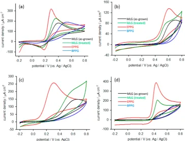
Figure 3.Cyclic voltammograms recorded at (a) treated and untreated MLGfilms in 1 M KCl (inset shows enlargement of scan obtained for untreated MLG), (b) MLG films, EPPG, and BPPG in 1 mM [Ru(NH3)6]3+ in 1 M KCl, (c) MLG films, EPPG, and BPPG in 1 mM
been transferred to Si/SiO2 wafers (see Figure S3 in the Supporting Information), but nothing can be inferred from this data regarding surface oxygen because the signal also measures oxygen on the surface of the wafer. Despite this, the spectrum is somewhat useful in that it shows no evidence of nickel or iron residue, indicating an extremely effective etching and transfer procedure. This is important because metal contamination could affect electrochemical properties, as has been reported elsewhere for carbon nanotubes.35
Cyclic voltammetry was used to probe the electrochemical properties of MLG, both in terms of its charging characteristics and its ET behavior with respect to standard redox probes. Figure 3a shows a comparison between charging currents recorded for as-grown and plasma-treated graphene films in potassium chloride solution. Before discussing the charging characteristics, it is worth noting the absence of any indication of residual nickel in the transferredfilms. It was observed that, when the samples were not etched with sufficient care, there was an oxidation peak around +0.1 V caused by residual metal (see Figure S4 of the Supporting Information). The responses in thefigure show the efficacy of the employed etching process, which is of great importance as residual catalyst can influence electron transfer properties with respect to certain redox probes, or obscure signals associated with probes which are active at similar potentials. Returning to the subject of charging, it is clear that plasma treatment increases the capacitive current required to charge the interface. This effect is attributed to faradaic contributions caused by the increased coverage of ionizable hydroxyl and carboxylic species, sometimes referred to as a“pseudocapacitance”. Such processes have been known to contribute to the large charging currents observed at carbon nanotube electrodes.36It is significant that, despite the increase in background charging current, these values are not so high as to be problematic for sensing, being, for example, an order of
magnitude lower than reported values for carbon nanotube electrodes.37
[image:4.625.129.494.68.345.2]that there have been some reports questioning its suitability for this purpose. While it can be useful in elucidating the nature of a surface, it is neither“simple”nor well-behaved,43and Patel et al.19have warned that it should be used with caution.
In order to show the functionalization of the MLG surface by plasma treatment, the Fe3+/2+probe was used. The kinetics of this redox process are known to be strongly influenced by the presence of surface oxides.12In fact, the presence of oxygenated functionalities on the electrode surface causes the mechanism of the redox process to change from outer- to inner-sphere.44It can be seen from Figure 3d that there is a considerable enhancement of the response at the treated MLG surface. While there is also an enhancement at EPPG relative to BPPG, this is attributed to oxygenated functionalities on the EPPG surface occurring naturally due to air exposure. These are not removed by the polishing procedure. On the other hand, the BPPG surface is freshly cleaved before measurements, and can therefore be reasonably assumed to have a relatively low oxide coverage, as evidenced by the extremely lethargic response of the Fe3+/2+probe.
Having shown, using standard redox probes, how the electron transfer properties of MLG can be enhanced using oxygen plasma treatment, the question of its suitability for sensing applications can be addressed. To this end, a number of biologically relevant analytes were tested. Figure 4 shows voltammetric responses measured for dopamine, NADH, ascorbic acid, and uric acid at as-grown and plasma-treated MLG films, along with control experiments involving commercially available EPPG and BPPG electrodes. In all cases, treatment was found to improve the response at MLG, with increased peak currents and lower detection potentials. The extent of this improvement was different for each molecule, since each is sensitive to different electrode features. NADH, for example, is relatively insensitive to oxygenated functionalities. The most important parameter for this biomolecule is the density of electronic states near the Fermi level.45 The slight decrease in oxidation onset potential observed suggests that plasma treatment increases the density of states for graphene. The oxidation of ascorbic acid is an
“inner-sphere” process, the kinetics of which are sensitive to surface microstructure, and not to functional groups.46 The improved sensitivity of the treated MLG to this probe can therefore be attributed to the increased coverage of edge-plane sites and defects. Uric acid, on the other hand, is known to be highly sensitive to oxygenated species.47 The dramatic enhancement of the sensitivity of MLG to this compound is caused by the increased number of surface functionalities. It is worth noting that uric acid is negatively charged at neutral pH,48 and might therefore be expected to experience some electrostatic repulsion at the heavily functionalized MLG surface. However, the findings shown here indicate that the probe’s sensitivity to oxygenated functionalities is sufficient to overcome this.
While the results presented here support the view that graphene grown using CVD is unsuitable for applications in electroanalytical sensing, it has also been shown that the ET properties of MLG can be greatly improved using a simple plasma treatment. Nonetheless, it is important to note that, for all of the analytes studied, the sensitivity of the modified MLG is eclipsed by commercial EPPG electrodes. Only in the case of uric acid can MLG be deemed genuinely competitive. It is therefore recommended that plasma-treated MLG should be considered as a viable alternative to EPPG in the detection of
analytes which are sensitive to oxygenated moieties, considering its low cost, disposability, and ease of production. We are currently attempting to extend these studies to thinner graphene samples, i.e., those which are mostly monolayer, in order to probe the influence of thickness on graphene’s ET properties.
4. CONCLUSIONS
Multilayer graphene films were grown on nickel foil and successfully transferred to PET for the elucidation of electroanalytical sensing properties. Rigorous physical charac-terization showed the transferred as-grownfilms had a very low coverage of defects and surface functional groups, and exhibited no traces of residual metal from either etchant or growth catalyst. A simple oxygen plasma treatment was introduced to increase the prevalence of defects and surface oxides. Standard redox probes and biologically relevant molecules were employed to demonstrate an overall enhancement of electron transfer behavior. This improvement is sufficient to show that graphene may be considered as a viable alternative to EPPG in electroanalysis, particularly in the detection of analytes which are sensitive to oxygenated species on the electrode surface. Thesefindings constitute a significant contribution towards the clarification of graphene’s heterogeneous electron transfer properties, with a view to its eventual applications in sensors, fuel cells, and energy conversion.
■
ASSOCIATED CONTENT*
S Supporting InformationVoltammetry of MLG on Ni growth substrate, de-convoluted XPS of MLG on Ni, XPS of MLG on Si/SiO2, and voltammetry of improperly transferred MLG (PDF). This material is available free of charge via the Internet at http://pubs.acs.org.
■
AUTHOR INFORMATIONCorresponding Author
*E-mail: [email protected].
Notes
The authors declare no competingfinancial interest.
■
ACKNOWLEDGMENTSThis research was supported by funding received from the Irish Research Council for Science, Engineering and Technology (IRCSET), co-funded by Marie Curie Actions under FP7. N.McE. and G.S.D. thank Science Foundation Ireland under Contract No. PI_10/IN.1/I3030 and the European Union under FP7-2010-PPP Green Cars (Electrograph No. 266391).
■
REFERENCES(1) McCreery, R. L.Chem. Rev.2008,108, 2646.
(2) Dumitrescu, I.; Unwin, P. R.; Macpherson, J. V.Chem. Commun.
2009, 6886.
(3) Keeley, G. P.; McEvoy, N.; Kumar, S.; Peltekis, N.; Mausser, M.; Duesberg, G. S.Electrochem. Commun.2010,12, 1034.
(4) Keeley, G. P.; McEvoy, N.; Nolan, H.; Kumar, S.; Rezvani, E.; Holzinger, M.; Cosnier, S.; Duesberg, G. S. Anal. Methods2012, 4, 2048.
(5) McEvoy, N.; Peltekis, N.; Kumar, S.; Rezvani, E.; Nolan, H.; Keeley, G. P.; Blau, W. J.; Duesberg, G. S.Carbon2012,50, 1216.
(6) Ratinac, K. R.; Yang, W.; Googing, J. J.; Thordarson, P.; Braet, F. Electroanalysis2011,23, 803.
(8) Shao, Y.; Wang, J.; Wu, H.; Liu, J.; Aksay, I. A.; Lin, Y. Electroanalysis2010,22, 1027.
(9) Brownson, D. A. C.; Banks, C. E.Analyst2010,135, 2768. (10) Chen, D.; Tang, L.; Li, J.Chem. Soc. Rev.2010,39, 3157. (11) Brownson, D. A. C.; Banks, C. E.Phys. Chem. Chem. Phys.2012, 14, 8264.
(12) Li, Z. J.; Xia, Q. F.Rev. Anal. Chem.2012,31, 57.
(13) Keeley, G. P.; O’Neill, A.; McEvoy, N.; Peltekis, N.; Coleman, J. N.; Duesberg, G. S.J. Mater. Chem.2010,20, 7864.
(14) Keeley, G. P.; O’Neill, A.; Holzinger, M.; Cosnier, S.; Coleman, J. N.; Duesberg, G. S.Phys. Chem. Chem. Phys.2011,13, 7747.
(15) Keeley, G. P.; O’Neill, A.; Holzinger, M.; Cosnier, S.; Coleman, J. N.; Duesberg, G. S.Technology2013,1, 58.
(16) Lim, C. X.; Hoh, H. Y.; Ang, P. K.; Loh, K. P.Anal. Chem.2010, 82, 7387.
(17) Brownson, D. A. C.; Gorbachev, R. V.; Haigh, S. J.; Banks, C. E. Analyst2012,137, 833.
(18) Zhang, B.; Fan, L.; Zhong, H.; Liu, Y.; Chen, S.J. Am. Chem. Soc.
2013,135, 10073.
(19) Patel, A. N.; Collignon, M. G.; O’Connell, M. A.; Hung, W. O. Y.; McKelvey, K.; Macpherson, J. V.; Unwin, P. R.J. Am. Chem. Soc.
2012,134, 20117.
(20) Goh, M. S.; Pumera, M.Anal. Chem.2010,82, 8367. (21) Valota, A. T.; Kinloch, I. A.; Novoselov, K. S.; Casiraghi, C.; Eckmann, A.; Hill, E. W.; Dryfe, R. A. W.ACS Nano2011,5, 8809.
(22) Ambrosi, A.; Pumera, M.J. Phys. Chem. C2013,117, 2053. (23) Keeley, G. P.; Lyons, M. E. G.Int. J. Electrochem. Sci.2009,4, 794.
(24) Banks, C. E.; Compton, R. G.Analyst2006,131, 15. (25) Ferrari, A. C.; Meyer, J. C.; Scardaci, V.; Casiraghi, C.; Lazzeri, M.; Mauri, F.; Piscanec, S.; Jiang, D.; Novoselov, K. S.; Roth, S.; Geim, A. K.Phys. Rev. Lett.2006,97, 187401.
(26) Chou, A.; Böcking, T.; Singh, N. K.; Gooding, J. J. Chem. Commun.2005, 842.
(27) Holloway, A. F.; Toghill, K.; Wildgoose, G. G.; Compton, R. G.; Ward, M. A. H.; Tobias, G.; Llewellyn, S. A.; Ballesteros, B. N.; Green, M. L. H.; Crossley, A.J. Phys. Chem. C2008,112, 10389.
(28) Landis, E. C.; Klein, K. L.; Liao, A.; Pop, E.; Hensley, D. K.; Melechko, A. V.; Hamers, R. J.Chem. Mater.2010,22, 2357.
(29) Rice, R. J.; McCreery, R. L.Anal. Chem.1989,61, 1637. (30) Moore, R. R.; Banks, C. E.; Compton, R. G.Analyst2004,129, 755.
(31) Desimoni, E.; Casella, G. I.; Morone, A.; Salvi, A. M. Surf. Interface Anal.1982,53, 627.
(32) Xie, Y.; Sherwood, P. M. A.Appl. Spectrosc.1989,43, 1153. (33) Xie, Y.; Sherwood, P. M. A.Chem. Mater.1990,2, 293. (34) Leiro, J. A.; Heinonen, M. H.; Laiho, T.; Batirev, I. G.J. Electron Spectrosc. Relat. Phenom.2003,128, 205.
(35) Pumera, M.Langmuir2007,23, 6453.
(36) Barisci, J. N.; Wallace, G. G.; Baughman, R. H.J. Electrochem. Soc.2000,147, 4580.
(37) Keeley, G. P.; Lyons, M. E. G.Int. J. Electrochem. Sci.2009,4, 794.
(38) Chen, P.; Fryling, M. A.; McCreery, R. L.Anal. Chem.1995,67, 3115.
(39) Rice, R. J.; McCreery, R. L.Anal. Chem.1989,61, 1637. (40) Alwarappan, S.; Erdem, A.; Liu, C.; Li, C.-Z.J. Phys. Chem. C
2009,113, 8853.
(41) Bowler, R.; Davies, T. J.; Hyde, M. E.; Compton, R. G.Anal. Chem.2005,77, 1916.
(42) Banks, C. E.; Davies, T. J.; Wildgoose, G. G.; Compton, R. G. Chem. Commun.2005, 829.
(43) McCreery, R. L.; McDermott, M. T. Anal. Chem. 2012, 84, 2602.
(44) Wong, C. H. A.; Pumera, M.Electrochem. Commun.2012,22, 105.
(45) Banks, C. E.; Compton, R. G.Analyst2005,130, 1232. (46) Hadi, M.; Rouhollahi, A.; Yousefi, M.; Taidy, F.; Malekfar, R. Electroanalysis2006,18, 787.

![Figure 3. Cyclic voltammograms recorded at (a) treated and untreated MLG[Fe(CN) films in 1 M KCl (inset shows enlargement of scan obtained foruntreated MLG), (b) MLG films, EPPG, and BPPG in 1 mM [Ru(NH3)6]3+ in 1 M KCl, (c) MLG films, EPPG, and BPPG in 1 mM6](https://thumb-us.123doks.com/thumbv2/123dok_us/1018360.616827/3.625.68.542.230.502/figure-voltammograms-recorded-treated-untreated-enlargement-obtained-foruntreated.webp)