Analysis of negative differential conductance in a two-island Coulomb
blockade system by a polytope approximation in phase space
Gareth J. Evans
Microelectronics Research Centre, Cavendish Laboratory, Madingley Road, Cambridge CB3 OHE, United Kingdom
H. Mizutaa)
Hitachi Cambridge Laboratory, Cavendish Laboratory, Madingley Road, Cambridge CB3 OHE, United Kingdom and CREST, Japan Science and Technology (JST), Shibuya TK Bldg., 3-13-11 Shibuya, Shibuya-ku, Tokyo 150-0002, Japan
共Received 14 March 2002; accepted for publication 25 June 2002兲
A two-island single-electron tunneling system is presented that exhibits negative differential conductance共NDC兲based on Coulomb blockade. The NDC mechanism is explained by introducing a simple analysis method, the polytope approximation. A condition for NDC to occur is analyzed fully by using the polytope approximation. © 2002 American Institute of Physics.
关DOI: 10.1063/1.1500786兴
I. INTRODUCTION
Single-electron 共SE兲 effects based on the Coulomb blockade共CB兲 of charge allows the manipulation of current on a per-electron basis. This has stimulated research into the possibility of using such effects to represent one bit of infor-mation by a small number of electrons and is hoped to lead eventually to a new generation of digital logic technology. The authors in Refs. 1 and 2 propose interesting devices based on negative differential conductance共NDC兲.
This article consists of two strands; the first demon-strates, through numerical simulation, a simple two-island SE device that exhibits NDC. NDC is usually associated with quantum levels but, due to SE effects, NDC need does not require energy quantization.
In the second strand, a simple analysis tool, called the
polytope approximation, is proposed that neatly describes the
reason for NDC and is used to derive a condition for NDC to occur. The polytope approximation is used to predict NDC valley positions and currents, both of which compare favor-ably with simulations.
Previously, Nakashima and Uozumi have demonstrated NDC in a linear array of seven3 and a nine4 islands in the context of a zig-zag conduction path through a granular sys-tem between two electrodes. The results were explained in terms of the competition between the forward rates of injec-tion of charge into the array with increasing bias and the reduction of the tunneling rate across a junction that is against the electric field set up by the source–drain bias and so this rate reduces with increasing bias.
Shin et al.5,6 demonstrate a different form of NDC in closed rings of islands 共the simplest being four islands兲. In this system, stable configurations of electrons can exist on the islands that form a ‘‘crystallike’’ structure and only when the bias has increased sufficiently to ‘‘melt’’ the crystal can current flow until a different stable configuration occurs. At
T⫽0 K, this leads to multiple zero-current regions as the source–drain bias increases, while at finite temperatures, it exhibits finite current and NDC.
Heij et al.7take a simpler approach and attach a SE box to the gate of a SE transistor共SET兲and demonstrate that the system will exhibit NDC for a range of conditions. The elec-trons in the box act as an additional gate bias to the SET and by biasing the SET and box in the appropriate range, the phase of the SET oscillation can be modified to produce NDC when an extra electron tunnels into/out of the box. A similar system is analyzed by Shin et al.8 in the context of coupled SETs though the possibility of it generating NDC is not discussed.
SE devices show an extreme sensitivity to stray共 uncon-trolled兲 charge in the surrounding environment 共the
offset-charge problem兲, but we will assume that a suitable fabrica-tion process lets us control this. Under these circumstances, NDC devices may be a useful component of future SE logic systems.
II. TWO-ISLAND COULOMB BLOCKADE SYSTEM
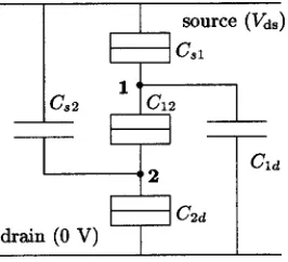
The circuit that will be analyzed is shown in Fig. 1 and is similar to Heij7 et al.’s system in that it has two islands,
but, like Nakashima and Uozumi’s3,4device, is arranged lin-early such that electrons have to pass through both islands. We assume that islands are metallic and that their tunnel resistances and capacitances are independent of bias.
Despite its apparent simplicity, the system exhibits a va-riety of complex behaviors as the capacitances and the tunnel resistances are varied. However, this article only examines a simple case where all the tunnel resistances are set to 106 ⍀. The system exhibits NDC over a wide range of circuit pa-rameters.
This circuit is the most general linear two-island circuit. Capacitances in parallel to the tunnel junctions can be merged together; capacitances to external gates are merged into the island-to-drain capacitance and the offset charge on the island changed appropriately.
a兲Electronic mail: [email protected]
3124
As an example of a system that demonstrates NDC, we set Cs1⫽C12⫽Cd2⫽0.1 aF, Cs2⫽6 aF, and Cd1⫽1 aF; the offset charge on islands 1 and 2 are denoted by q1 and q2
which are assumed to be in units of e. The results are
gen-erated using a Master equation simulator ignoring
cotunneling.9Later, a condition for NDC will be derived. In this situation, Vds acts as a gate on the second island—producing oscillations in its transfer characteristics, and hence NDC. Eventually, the bias over the second tran-sistor is sufficient high that the gate looses control.
The current as a function of Vds and of q1 is shown in Fig. 2. q2 has been set as⫺0.5 and, qualitatively, the only
change in the characteristics as q2 varies is that the phase of
the oscillation changes. Clear NDC can be seen for a small range of the values of q1; this demonstrates the extreme
[image:2.612.109.242.52.173.2]sensitivity of the characteristic on the offset charge. A change of only a small fraction of an electron charge can change the NDC current by many orders of magnitude or move the sys-tem to a non-NDC region.
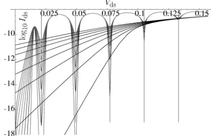
Figure 7 shows the Ids– Vds characteristics at
tempera-tures between 8.2 to 1.2 K in 1 K steps. The NDC regions exhibit peak-to-valley ratios of up to 1010at 4.2 K. The peak heights for higher biases tend to be only weakly dependent on temperature while the valley currents are much more strongly dependent. This view is shown even more clearly for the different offset charge configuration (⫺0.4,⫺0.5) which is shown in Fig. 8. Higher temperatures broaden the peaks, gradually washing them out.
Comparing Figs. 7 and 8, it is clear that the offset charge change of only⌬q1⫽0.15共remembering that the character-istics are periodic in q1 and q2兲has produced peaks that are a couple of orders of magnitude higher, while also degrading the quality of the peaks.
As a consequence, any logic device relying on the order of magnitude of the current would have to control q1 to
Ⰶ0.15, while the phase of the peaks is controlled by q2 and
a change of 0.5 produces a phase shift of.
III. ANALYSIS BASED ON THE POLYTOPE APPROXIMATION
In this section, q˜, the phase space for the system, is introduced. A simple non-NDC example is used to motivate an approximation to the full Master equation solution to the current. Using this polytope10approximation, the explanation
of NDC is simply described. The condition for NDC to occur is then derived from this interpretation and the system is related to the device of Nakashima et al.3,4
The transition rate in Orthodox Theory11for a hole tun-neling through a tunnel resistance Rklfrom island k to island
ᐉ is,
⌫kl⫽ 1
e2Rkl
⫺⌬Ekl 1⫺exp共⌬Ekl/kT兲
, 共1兲
where the change in free energy⌬Ekl can be expressed as,
⌬Ekl⫽ e2
2 ⑀kl T
C⫺1⑀
kl⫹e2⑀kl T
C⫺1˜q⫺eV
kk⫹eVᐉᐉ 共2兲
and each island i is represented by the ith element of the vectors. Cis the共symmetric兲capacitance matrix and Ci j is the negative sum of the capacitances joining islands i and j while Cii is the positive sum of all the capacitances con-nected to island i. (⑀kl)i⫽⫺␦ik⫹␦iᐉand␦i j is zero if j is a bias.i is unity if i represents a bias, otherwise is zero. The operatorT is the transpose of the vector.
The dynamics of the system are Markovian and for a fixed Vds the state of the system is fully characterized by
(q˜)i⫽qi⫹⌺Ci⬘iVi⬘/e, where qi⫽ni⫹qi
0
/e, the number of holes on island i is ni, the fractional offset charge induced on the island is qi0, and the sum i
⬘
runs over the capacitances/tunnel resistances connecting i to bias/gate i⬘
at potential Vi⬘.For the two-island system with the drain grounded, then,
C⫽
冉
C1⌺ ⫺C12
⫺C12 C2⌺
冊
, ˜q⫽冉
q1⫹Cs1Vds/e q2⫹Cs2Vds/e
冊
,
where C1⌺⫽Cs1⫹C12⫹Cd1, etc. Clearly the point describ-ing the system (q˜) moves at a velocity of (Cs1,Cs2)T/e from a start point (q1,q2)T.
The set of⑀kᐉneeded to move a hole from the source (s) to the drain (d) are s→1:⑀s1⫽(1,0)T, 1→2:⑀12
⫽(⫺1,1)T, 2→d:⑀2d⫽(0,⫺1)T. If a transition k→ᐉ is
taken then q˜→˜q⫹⑀kᐉand so a lattice of states is formed in q˜ space. The current may then be calculated by a Master equa-tion connecting these lattice states using the formulas共1兲and
共2兲. A sequence of current-producing transitions make the system hop round a loop in the lattice.
FIG. 1. Two-island CB system.
[image:2.612.54.295.580.723.2]For far-time dc characteristics, the initial lattice point that the system starts at is irrelevant as it will diffuse through the lattice and so the current is periodic in q˜ with the lattice spacing 共unity兲. The polytope approximation assumes that this diffusion process takes the system to a set of loops in-volving a single state and that the transition rate out of this state dominates the current flow produced by any of the loops going through it. The dynamics of SE systems act such that if a particular transition⑀kᐉ from a state q˜ is taken then the transition rate for it being taken again from the new state (q˜⫹⑀kᐉ) is less (⌫kᐉ关˜q兴⬎⌫kᐉ关˜q⫹⑀kᐉ兴). Hence, the dynam-ics do indeed tend to confine the system to a small part of phase space.
A region of sub-Ithcurrent is constructed geometrically
by calculating the regionQwhere all transition rates are less than Ith/e. Each point in q˜ space may now be classified as
sub-Ith if one共or more兲of the points of the lattice that it is
part of lies within Q. In this way, a set of regions of sub-Ith
current is constructed and a lattice formed by translations of Q. As the system is periodic, only a single n cube of the space need be considered and this will be taken to be that centered at the origin and shall be denoted as Q0.
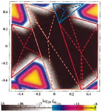
Figure 3 shows log10关Ids(q˜)兴for a more capacitively
ho-mogeneous system. Surfaces of constant current are reason-ably well approximated by polytopes, though there are neck points where the overall current is lower; the necks appear where two or more polytopes are in close proximity. The polytopes for 1 fA current are drawn; the original polytopes overlapped so a set of nonoverlapping polytopes were gen-erated that covered the same area, these are drawn with solid boundaries and their interiors are marked by the dashed lines.
The polytope approximation, despite being so simple, tends to be conservative in which regions of phase space it assigns as sub-Ith, in that in all of the examples that the
authors have studied, the true sub-Ithregion is a superset of
the region that the polytope approximation provides. Strongly inhomogeneous tunnel resistances tend to lead to extra polytopelike regions that need further corrections to describe them. It is more difficult to test the validity of the polytope approximation in higher dimensions共more than two islands兲but the terminology used in this paper is that for the general n-dimensional system in anticipation for such an ex-tension.
A consequence of the polytope approximation is that, for a particular Vds, the volume ofQ0共in dimensionless units兲is
at least the probability that a device with a random offset charge configuration 共uniformly distributed in the range ⫺0.5 to 0.5兲will have a threshold voltage below Vds.12,13
IV. GEOMETRICAL EXPLANATION FOR NEGATIVE DIFFERENTIAL CONDUCTANCE IN THE TWO-ISLAND SYSTEM
The phase space diagram of the two-island system for various values of Vds is shown in Fig. 4. Each line of three
diagrams are evenly spaced in Vds, there is a large jump in Vdsfrom one row to the other.
The polytope for this system is long and thin in the q2
direction and wraps round many times. The polytopes drawn on the diagrams are for Ith⫽1 fA, the shading is indicative of
the log10(Ids) and the range of each diagram is from⫺0.5 to ⫹0.5 in both directions. The system point starts at (0.4, ⫺0.5) and moves along the thick green line. Thus, in the top left-hand side diagram, the system is in a sub-Ith region, the next in an above-Ith region and the next again in a sub-Ith region—thus, the system has gone through one current peak. We note that the trajectory of the system has wrapped round due to the periodic dependence on q˜.
The system travels very quickly in the q2 direction,
lap-ping the polytope many times while at the same time, the left-hand side edge of the polytope gradually moves to the right-hand side. The bottom set of diagrams show that poly-tope decreases in size until eventually it will disappear.
The non-NDC part of Fig. 2 can also be explained. Take for example the center point 共0, 0兲. As Vdsincreases, then it
moves quickly in the q2direction, lapping many times,
how-ever, as the polytope at that point is all sub-Ith, then, the
current is sub-Ithuntil suddenly the left-hand side boundary
of the polytope runs past it and it has a significant current.
V. GEOMETRICAL CONDITION FOR NEGATIVE DIFFERENTIAL CONDUCTANCE
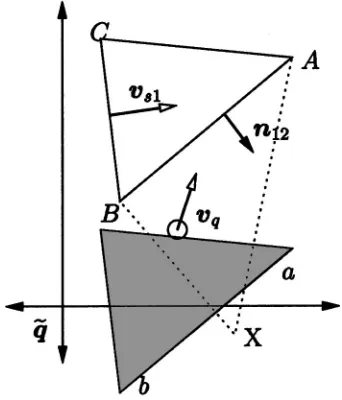
We define that a device exhibiting NDC has a current that falls from above Ith to below Ith as Vds increases i.e.,
[image:3.612.93.258.53.236.2]苹V:关dI(V)/dVds⬍0 and I(V)⫽Ith兴. This is a more specific definition of NDC than usually used (苹V:dI(V)/dVds⬍0). A necessary condition for NDC is that the system can head from a point outside the polytope共with I⬎Ith兲into the polytope 共where I⬍Ith兲. Thus, the system must move faster toward a polytope boundary faster than the boundary re-cedes. This can be done for each face and can be used to construct a region of phase space (q˜) that can hit the face before it completely disappears—thus providing a criterion under which at least one dip of at least Ithcan occur. FIG. 3. 共Color兲 Structure: Cs1⫽C12⫽Cd2⫽1 aF, Cd1⫽1.5 aF and Vds
⫽0.01 V. The log10of the current is plotted using the scale shown as a function of q˜. Note the periodicity of the characteristic and that surfaces of
The phase-space diagram for a voltage Vds is drawn in
Fig. 5, the sub-Ith region is the triangle ABC, the shaded
triangle is one of the images of ABC due to the periodicity in q
˜ space. The transition s→1 corresponds to the edge BC and this is the only edge that moves, and its velocity isvs1. The edge AB corresponds to the interisland transition 1→2, while CA is the transition 2→d. The normal to the face AB
is n12. The system is described by the point q˜, indicated by
the circle, and travels at velocityvq⫽(Cs1,Cs2)T/e. The triangle ABC gradually shrinks until it disappears to the point A at a voltage Vdsmax. All points in the triangle AXB will have flowed through AB by this time and so will have experienced at least one section of NDC between Vds and Vdsmaxas they move from a point outside the triangle共where
I⬎Ith兲 to inside (I⬍Ith). Those points that also cross
through ab will have two NDC sections with I⬎Ith. The outward pointing normal to the region for a transi-tion ⑀kᐉ is ⫺C⫺1⑀
kᐉ, and so a necessary condition for the system to be able to go through face AB is thatvqis directed oppositely to the outward normal to AB (n12),
vq•n12⬍0
共Cs1,Cs2兲
冉
C2⌺⫺C12 C12⫺C1⌺
冊
⬍0
共3兲
Cs2共Cs1⫹Cd1兲⬎Cs1共Cs2⫹Cd2兲
Cd1 Cs1⬎
Cd2 Cs2.
Similarly, the condition for the system to be able to go through BC is,
vq•共⫺ns1兲⫺兩vs1兩⬎0
共Cs1,Cs2兲•
冉
C2⌺C12
冊
⫺共C1⌺C2⌺⫺C12 2 兲⬎
0
共4兲
Cs1C2⌺⫹Cs2C12⫺C1⌺C2⌺⫹C122 ⬎0
⫺Cd1C2⌺⫺C12Cd2⬎0, which can never be satisfied.
Doing the same for edge CA,
vq•n2d⬍0
共Cs1,Cs2兲•
冉
C12C1⌺
冊
⬍0 共5兲Cs1C12⫹Cs2C1⌺⬍0,
which again can never happen共geometrically, this is because the outward normal and the system velocity are both lie in the same quadrant兲.
[image:4.612.319.562.448.680.2]Thus, the system can only travel fast enough toward the face AB and to do this it must obey Eq. 共3兲. The physical interpretation of this is that the transition rate corresponding
FIG. 4. 共Color兲Phase space diagrams for an NDC system. The polytopes have solid boundaries and their interi-ors are marked by dashed lines. Vdsin the top row of diagrams are 10.5, 21.0, and 31.5 mV共left- to right-hand side兲, while Vdsfor the bottom rows are 105, 115, and 126 mV. The system point starts at (0.4,⫺0.5) and moves along the thick green line共that is almost ver-tical兲. As Vds increases from one dia-gram to the next, the line moves out of a subthreshold共1 fA兲region and back again. The bottom set of diagrams shows the system shortly before the polytope disappears and all points have above threshold current.
[image:4.612.88.259.481.681.2]to the interisland transition (1→2) decreases with
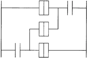
increas-ing Vds. The condition共3兲implies that Fig. 1 can be redrawn
more suggestively as Fig. 6 which now is reminiscent of Nakashima and Uozumi’s3,4 configuration—indeed, this is the simplest zig-zag pattern possible. Island one couples more strongly to the drain and island two to the source, this means that the potential drop across the central tunnel resis-tance is in an energetically unfavorable direction for holes to tunnel from island one to island two en route from source to drain.
The condition 共3兲 is a necessary condition under the polytope approximation even in the case when the polytopes from adjacent lattice points overlap because the resultant above-Ith region is bounded by line segments that have the
same normals and velocities as the polytopes making it up 兵ns1,n12,n2d其. As a consequence, the condition required is
identical.
Relaxing the definition for NDC to the most general case (苹V:dI(V)/dVds⬍0) still delivers the same condition as it
is independent of the choice of Ith.
As an aside, the parameters can be chosen such that the system point moves parallel to the edge AB of the polytope and thus the current remains constant while this is the domi-nant edge. Trivially, the condition to produce this constant current step is obtained by setting the inequality of Eq.共3兲to equality.
The polytope method implies that the prediction of the minimum current is an easily accessible quantity. In general, it is difficult to write analytic formulae for these currents due to the periodicity of the space. However, in our specific ex-ample, then the minimum current should be when the transi-tion rate for processes ⑀2d and⑀12 are identical.
If both tunnel resistances are identical then, this is equivalent to saying their transition energies are identical:
⑀2d
T
C⫺1˜q⫹ 1 2⑀2d
T C⫺1⑀
2d⫽⑀12
T
C⫺1˜q⫹ 1 2⑀12
T C⫺1⑀
12
共⑀2d
T ⫺⑀12
T兲
C⫺1˜q⫽⫺12关⑀2d
T
C⫺1⑀2d⫹⑀12
T
C⫺1⑀12兴
共6兲
e2
兩C兩
冉
2C12⫺C2⌺
⫺C12⫹2C1⌺
冊
•q ˜⫽e
2共C
2⌺⫺C12兲
2兩C兩
冉
2C12⫺C2⌺⫺C12⫹2C1⌺
冊
•˜q⫽C2⌺⫺C12
2 ,
this line intersects the system velocity point q˜⫽(q1,q2)
⫹(Cs1,Cs2)Vds/e when,
Vds⫽e
•共C2⌺⫺C12兲/2⫺关q1共2C12⫺C2⌺兲⫹q2共⫺C12⫹2C1⌺兲兴 Cs1共2C12⫺C2⌺兲⫹Cs2共⫺C12⫹2C1⌺兲
,
共7兲 and so the coefficient of q2 is the period of the oscillations,
⌬Vds⫽e•
⫺C12⫹2C1⌺
Cs1共2C12⫺C2⌺兲⫹Cs2共⫺C12⫹2C1⌺兲
⫽ e
Cs2•
1
1⫺Cs1
Cs2•
C2⌺⫺2C12
2C1⌺⫺C12
,
for our example system this gives 0.0279 V which is within error margins of the numerical simulation. The second factor in this term increases the period by ⬇4.5% compared to
e/Cs2.
The Vds positions of the valleys can also be found from
Eq.共7兲though care is needed to cope with the periodicity of the space. These are shown by the vertical red lines in Figs. 7 and 8. From their intersection points, the current can also be estimated and these are draw using black lines on the figures.
[image:5.612.97.254.52.156.2]The agreement of valley positions is excellent, however, the current predictions are too high by about a factor two for Fig. 7 and, for some cases in Fig. 8, by over an order of magnitude. This poor agreement is due to the breakdown of the assumptions of the polytope approximation. In these cases, there are at least two loops of states and the lowest transition rate step may not be the limiting factor of the loop as reverse transition rates 共holes hopping backwards兲 may limit the current.
VI. CONCLUSIONS
[image:5.612.320.556.52.205.2]This article has introduced the polytope approximation as a tool to analyze the behavior of SE systems. It has been used to demonstrate that a two-island SET system with no quantum energy levels can exhibit NDC due to CB. Further-more, from a purely geometric point of view, a condition for
FIG. 6. The circuit remapped to a zig-zag path.
[image:5.612.67.300.622.731.2]NDC has been derived by showing that the system must move through phase space at sufficient velocity that it can pass through one of the faces of the polytope. This leads to an algebraic condition for NDC.
1K. Maezawa, T. Akeyoshi, and T. Mizutani, IEEE Trans. Electron Devices
41, 148共1994兲. 2
H. J. Levy and T. C. McGill, IEEE Trans. Neural Netw. 4, 427共1993兲. 3H. Nakashima and K. Uozumi, Jpn. J. Appl. Phys., Part 2 34, L1659
共1995兲.
4H. Nakashima and K. Uozumi, J. Vac. Sci. Technol. B 15, 1411共1997兲. 5
M. Shin, S. Lee, K. W. Park, and E. H. Lee, J. Appl. Phys. 84, 2974 共1998兲.
6M. Shin, S. Lee, K. W. Park, and E. H. Lee, Phys. Rev. Lett. 80, 5774 共1998兲.
7C. P. Heij, D. C. Dixon, P. Hadley, and J. E. Mooij, Appl. Phys. Lett. 74, 1042共1999兲.
8M. Shin, S. Lee, and K. W. Park, Phys. Rev. B 62, 9951共2000兲. 9M. Kirihara, K. Nakazato, and M. Wagner, Jpn. J. Appl. Phys., Part 1 38,
2028共1999兲.
10A polytope is the mathematical name for a finite volume polyhedron. In general, n-dimensional terminology will be used in this article—thus a plane关an (n⫺1)-dimensional object兴is a line in two dimensions, a vol-ume is an area in two dimensions, etc.
11Single Charge Tunneling, edited by H. Grabert and M. H. Devoret共 Ple-num, New York, 1992兲.
12
G. J. Evans, H. Mizuta, and H. Ahmed, Jpn. J. Appl. Phys., Part 1 84, 2974 共2001兲.
13G. J. Evans, Ph.D. thesis, University of Cambridge, 2002. FIG. 8. (⫺0.45,⫺0.5): log10Ids(Vds) characteristics at temperatures 8.2 K
[image:6.612.67.275.54.188.2]