LOW POWER TEST COMPATIBILITY CLASSES: EXPLOITING REGULARITY FOR
SIMULTANEOUS REDUCTION IN TEST APPLICATION TIME AND POWER DISSIPATION
Nicola Nicolici
Computer-Aided Design and Test Group
Dept. of Electrical & Computer Engineering
McMaster University
Hamilton, ON L8S 4K1, Canada
[email protected]
Bashir M. Al-Hashimi
Electronic Systems Design Group
Dept. of Electronics and Computer Science
University of Southampton
Southampton SO17 1BJ, U.K.
[email protected]
Abstract
Traditional DFT methodologies increase useless power dissipation during testing and are not suitable for test-ing low power VLSI circuits leadtest-ing to lower reliability and manufacturing yield. Traditional test scheduling ap-proaches based on fixed test resource allocation decrease power dissipation at the expense of higher test application time. On the one hand it was shown that power conscious test synthesis and scheduling eliminate useless power dissi-pation. On the other hand by exploiting regularity in BIST RTL data paths using test compatibility classes an improve-ment in test application time, BIST area overhead, perfor-mance degradation, volume of test data, and fault escape probability is achieved. This paper shows that when com-bining power conscious test synthesis and scheduling with the test compatibility classes into low power test compatibil-ity classes, simultaneous reduction in test application time and power dissipation is obtained.
1. Introduction
The demand for low power very large scale integrated (VLSI) circuits in the growth area of portable communi-cations will continue to increase in the future. Cost and lifetime cycle of near future portable communications and computing systems will depend not only on VLSI circuits designed using low power synthesis techniques, but also on new design for test (DFT) methods targeting power mini-mization during test application. This is because traditional DFT methods increase power dissipation during test appli-cation and are not suitable for testing low power VLSI cir-cuits leading to lower reliability and manufacturing yield. To avoid unnecessary iterations in the design flow, recent re-search interests have shifted towards addressing testability
during the early stages of the VLSI design flow [7]. A novel built-in self-test (BIST) methodology for register transfer-level (RTL) data paths using a new concept called test compatibility classes (TCC) which overcomes the problems of test application time, BIST area overhead, performance degradation, volume of test data, and fault-escape probabil-ity associated with traditional BIST embedding methodol-ogy [14, 15], was proposed recently in [20, 22]. To fully ex-ploit the testability benefits of BIST RTL data paths, power dissipation during test application in BIST RTL data paths needs to be accounted, and novel power conscious test syn-thesis and scheduling algorithms equally applicable to BIST embedding and TCC grouping methodologies need to be developed. This is of particular importance when power dissipation during the functional operation is not exceed-ing a given power constraint as it is the case for RTL data paths synthesized using low power high level synthesis al-gorithms [8, 10, 11]. Previous test scheduling alal-gorithms [4, 12, 13, 17, 18, 24, 23, 25] are not suitable for BIST RTL data paths due to the following three problems:
a. test scheduling assumes fixed amount of power dissi-pation associated with each test which is not the case for BIST RTL data paths;
b. test scheduling is performed on a fixed test resource allocation without considering the strong interrelation between test synthesis and test scheduling;
c. reduction in test application time is achieved at the ex-pense of higher power dissipation;
The aim of this paper is to show that when combin-ing power conscious test synthesis and test schedulcombin-ing al-gorithms with the test compatibility classes, simultaneous reduction in test application time and power dissipation is achieved with constant savings in BIST area overhead when compared to the traditional BIST embedding methodology. The rest of the paper is organized as follows. Sections 2 and 3 overview low power BIST for RTL data paths [21] and test compatibility classes [22]. Section 4 introduces new low power test compatibility classes. Experimental results and conclusions are given in Sections 5 and 6 respectively.
2. Low Power BIST for RTL Data Paths
This section gives a taxonomy of power dissipation dur-ing testdur-ing in BIST RTL data paths introduced in [21].
According to the necessity for achieving the required test efficiency, power dissipation is classified into necessary and useless power dissipation. Necessary power dissipation is the power dissipated in test registers and tested modules during each test session and the power dissipated in test registers while shifting in seeds for test pattern generators and shifting out responses from signature analyzers. Nec-essary power dissipation is compulsory for achieving the required test efficiency, however, the useless power dissi-pation must be eliminated using power conscious test syn-thesis and scheduling ([21] and Section 4). In order to de-fine useless power dissipation, firstly spurious transitions in BIST RTL data paths are introduced. A spurious transition when employing BIST for RTL data paths is a transition which occurs in modules and/or registers which are not used in the current test session. These transitions do not have any influence on test efficiency since the values at the input and output of modules and/or values loaded in registers are not useful test data. Useless power dissipation is the power dis-sipated in registers and untested modules due to spurious transitions which cannot be eliminated by any configuration of control signals of data path multiplexers.
According to the occurrence during the testing process power dissipation is classified into test application and shift-ing power dissipation. Test Application Power dissipation (TAP) is the power which occurs during execution of each test session when test patterns, necessary to achieve the required test efficiency, are applied to modules. Shifting
Power dissipation (SP) is the power which occurs while
shifting in the seeds for test pattern generators, required for next test session, and shifting out the responses stored in signature analyzers at the end of the previous test session. It should be noted that multiplexer power is low during test-ing since multiplexer control signals are modified only at the start and at the end of every test session, thus avoiding any glitching activity which can propagate from control logic.
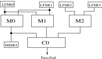
M0 M1 M2
C0
LFSR0 LFSR1 LFSR2 LFSR3
MISR4
[image:2.612.343.512.71.169.2]Pass/Fail
Figure 1. Test Compatibility Class
3. Test Compatibility Classes
This section summarizes test compatibility classes (TCC) that exploit the regularity of data path circuits to reduce test application time, BIST area overhead, perfor-mance degradation, volume of test data, and fault-escape probability [20, 22].
Example 1 To give an insight into the TCC grouping
methodology consider a small part of a complex data path as shown in Figure 1. The part of the data path has 3
mod-ules of module-type Mtypeand 5 registers. Each module is
annotated with its name (M0-M2). Since Mtypemodules are
instances of the same module library prototype, then they have identical physical and structural information and hence identical detection probability profile. Thus if test patterns
are applied to modules M0−M2simultaneously same fault
coverage is achieved when compared to applying test pat-terns in different test sessions. Note that LFSR0is the only
test register which applies test patterns to left input port of
M0and M1. Also LFSR2generates test patterns to left input
port of M2and needs to be initialized with the same seed
as LFRS0before beginning of the test session. The same
applies to LFSR1and LFSR3. When same test patterns are
generated by LFSR0and LFSR2at left input port (LFSR1
and LFSR3at right input port) of M0, M1, and M2,
identi-cal output responses are expected at the same time. Hence a
comparator C0is used to check the output responses. Only
a single signature analyzer MISR4is allocated to compress
the output responses of all the modules M0, M1, and M2
which are tested simultaneously. The signature analysis
reg-ister MISR4is necessary to detect faults in the case when
output responses of all the three modules M0, M1, and M2
are equal during the entire test application period but dif-ferent from the fault-free output response. The use of com-parators solves three problems. Firstly it reduces both BIST area overhead (1 MISR and 1 comparator vs. 3 MISRs) and performance degradation (1 MISR vs. 3 MISRs embedded in data path). Secondly it reduces fault-escape probabil-ity since faulty output responses which map into fault-free signatures in the BIST embedding methodology will be de-tected by the comparators. And thirdly, the number of signa-tures is reduced which has the following two implications: volume of test data is reduced which leads to less storage requirements and test application time is minimized due to less clock cycles needed to shift out the test responses.
4. Low Power Test Compatibility Classes
Power conscious test synthesis and scheduling described in [21] are equally applicable to both BIST embedding [15, 14] and TCC grouping methodologies [20, 22]. Power conscious test synthesis and scheduling are based on the analysis of the effect of test synthesis and scheduling on useless power dissipation (Section 2). Thereafter, test re-sources allocation (test synthesis) and module selection for concurrent testing (test scheduling) are done by power con-scious algorithms ACCEPT-MOVE and SELECT-MODULE described in [21]. The final step is to synthesize a BIST controller that controls the execution of test sessions, shifts in the seeds for LFSRs, shifts out the signatures stored
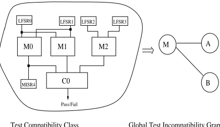
M0 M1 M2
C0
Global Test Incompatibility Graph Test Compatibility Class
LFSR0 LFSR1 LFSR2 LFSR3
MISR4
Pass/Fail
M A
[image:3.612.316.534.71.197.2]B
Figure 2. Single Test Compatibility Class Dur-ing Incremental Test SchedulDur-ing
in MISRs, and assigns proper values to multiplexer con-trol signals such that useless power is eliminated. In or-der to achieve minimum area overhead, the BIST controller is merged with the functional controller into a single con-trol unit for the data path. This section focuses only on the power conscious changes to the BIST hardware synthesis algorithm described in [22]. A detailed and self-contained explanation is given in [19].
To achieve maximum test concurrency it is required that a large number of different-type test compatibility classes are compatible. Therefore, a high number of incompatible modules are sought to be merged in a small number of in-compatible TCCs. This will reduce the number of edges in the global test incompatibility graph defined as follows. A global test incompatibility graph (G-TIG) is a graph where a node appears for every TCC. As shown in Figure 2 an edge exists between nodes M and A if test compatibility classes
for module types Mtypeand Atypeand are incompatible. Test
scheduling is performed using the global test incompatibil-ity graph. Fault sets of different-type modules have differ-ent detection probability profiles, and, hence, TCCs of dif-ferent module-types need difdif-ferent test application times to satisfy the required fault coverage. Thus, the incremental TCC scheduling algorithm deals with unequal test lengths. The test scheduling algorithm for partitioned testing with run to completion from [5] has been modified such that test scheduling and signature analysis registers allocation is done simultaneously [20, 22]. In order to increase test concurrency of test compatibility classes while satisfying a given power constraint two modifications to the incremental TCC scheduling algorithm [22, 19] are necessary:
• While generating the G-TIG for maximum test
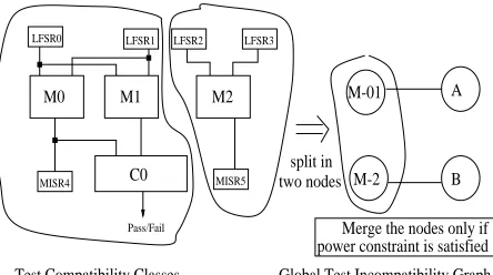
M0 M1 M2
C0
Global Test Incompatibility Graph
LFSR0 LFSR1 LFSR2 LFSR3
MISR4
Pass/Fail
A
B
Test Compatibility Classes
MISR5
M-01
M-2 split in two nodes
[image:4.612.57.279.71.195.2]Merge the nodes only if power constraint is satisfied
Figure 3. Two Test Compatibility Classes Dur-ing Incremental Test SchedulDur-ing
consisting of a single module. This will lead to higher number of nodes in the G-TIG. However the total nec-essary power dissipated by each TCC is lower. Thus instead of merging all the compatible modules prior to TCC scheduling, there are more nodes created in the G-TIG and they will be merged later if the power constraint is satisfied. Therefore, if two TCCs of the same type present in G-TIG are compatible then dur-ing the incremental test scheduldur-ing they are merged as explained in the following modification.
• During the simultaneous TCC scheduling and
signa-ture analysis allocation algorithm [22] if two test com-patibility classes are compatible then they are merged if they meet the given power constraint. This will lead to an incremental generation of maximal test concur-rency within the G-TIG only if power constraints are satisfied. The assignment of conflict free modules to TCCs is driven by power constraint and not by the in-crease in the size of the output register set as in the case of [22]. This causes both high test concurrency and satisfaction of power constraints at the expense of a decrease in the size of the output register set and hence the potential reuse of signature analysis registers.
The previous two modifications can be explained using
Figure 3. For example, module M2is not merged with
mod-ule M0and M1into a single test compatibility class (Figure
2) prior to the generation of the G-TIG and TCC scheduling.
Rather, two separate nodes are created in G-TIG (M−01
and M−2) (Figure 3). Only if if the power constraint is
satisfied the modules are merged into a single TCC. Other-wise, two test compatibility classes are required with small
area overhead due to MISR5. However, when compared
to BIST embedding methodology [15, 14] savings in BIST area overhead are preserved, as well as reduction in test ap-plication time as described in the experimental results.
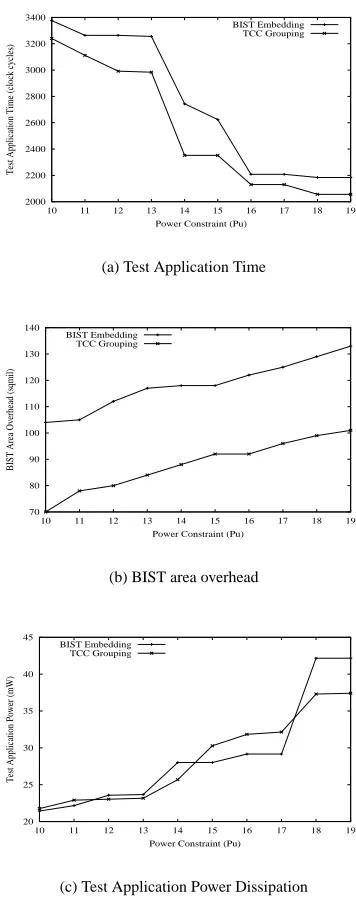
5. Experimental Results
To outline the advantages of combining the TCC group-ing methodology [22] with power conscious test synthesis and scheduling [21], Figures 4 and 5 give a comparison in terms of test application time (TAT), BIST area overhead (BAO), test application power (TAP), and shifting power (SP) for traditional BIST embedding [15, 14] and the TCC grouping [20, 22] methodologies. To show the suitability of TCC grouping for various power constraints, experiments were done on elliptic wave digital filter (Figure 4) and 32 point discrete cosine transform (Figure 5) using synthesized using the ARGEN high level synthesis system [9]. Test ap-plication time (TAT) for adders and multipliers are assumed to be T+=Tu, and respectively T∗=4×Tu, where Tu=128 for achieving 100% fault coverage for 8 bit data path mod-ules technology mapped into AMS 0.35 micron technology [1]. During the power conscious testable design space ex-ploration power dissipation for registers, adders and multi-pliers is assumed to be PREG=Pu, P+=Puand P∗=4×Pu,
where Puis a generic high level model for power
dissipa-tion that provides the flexibility of applying the proposed algorithms to various library modules with different power characterization. To validate the high level generic val-ues, using a real delay model simulator [16] and AMS 0.35 micron timing and power information operating at supply voltage 3.3V and clock frequency 100MHz, and hence ac-counting for glitching activity, the following values were obtained for 8 bit data path width using pseudorandom
se-quences applied during testing: PREG =0.8mW , PLFSR=
1mW , PMISR=2mW , PBILBO=2.5mW , P+=3.5mW , and
P∗=11.5mW .
applica-0 200 400 600 800 1000 1200 1400 1600 1800
10 11 12 13 14 15 16 17 18 19
Test Application Time (clock cycles)
Power Constraint (Pu) BIST Embedding
TCC Grouping
(a) Test Application Time
25 30 35 40 45 50
10 11 12 13 14 15 16 17 18 19
BIST Area Overhead (sqmil)
Power Constraint (Pu) BIST Embedding
TCC Grouping
(b) BIST area overhead
20 25 30 35 40 45 50
10 11 12 13 14 15 16 17 18 19
Test Application Power (mW)
Power Constraint (Pu) BIST Embedding
TCC Grouping
(c) Test Application Power Dissipation
9 10 11 12 13 14 15 16 17
10 11 12 13 14 15 16 17 18 19
Shifting Power (mW)
Power Constraint (Pu) BIST Embedding
TCC Grouping
[image:5.612.336.514.79.531.2](d) Shifting Power Dissipation
Figure 4. Comparison for elliptic waveform digital filter
2000 2200 2400 2600 2800 3000 3200 3400
10 11 12 13 14 15 16 17 18 19
Test Application Time (clock cycles)
Power Constraint (Pu) BIST Embedding
TCC Grouping
(a) Test Application Time
70 80 90 100 110 120 130 140
10 11 12 13 14 15 16 17 18 19
BIST Area Overhead (sqmil)
Power Constraint (Pu) BIST Embedding
TCC Grouping
(b) BIST area overhead
20 25 30 35 40 45
10 11 12 13 14 15 16 17 18 19
Test Application Power (mW)
Power Constraint (Pu) BIST Embedding
TCC Grouping
(c) Test Application Power Dissipation
4 5 6 7 8 9 10 11 12
10 11 12 13 14 15 16 17 18 19
Shifting Power (mW)
Power Constraint (Pu) BIST Embedding
TCC Grouping
[image:5.612.73.258.84.612.2](d) Shifting Power Dissipation
tion time and power dissipation is provided (problem (c) in Section 1). Reducing test application time and power dissi-pation simultaneously using TCCs is particularly important for high performance low power RTL data paths generated using low power high level synthesis algorithms [8, 10, 11].
6. Conclusions
Traditional power constrained test scheduling algorithms [4, 12, 13, 17, 18, 24, 23, 25] decrease power dissipation at the expense of higher test application time. This paper has shown that when combining power conscious test synthesis and test scheduling algorithms [21] with test compatibility classes [22] into low power test compatibility classes, si-multaneous reduction in test application time and power dis-sipation is obtained when compared to traditional BIST em-bedding methodologies for BIST RTL data paths [15, 14].
7
References
[1] AMS. 0.35 Micron CMOS Process Parameters. Austria Mikro Systeme International AG, 1998.
[2] P. Bardell, W. McAnney, and J. Savir. BuiltIn Self Test
-Pseudorandom Techniques. John Wiley & Sons, 1986.
[3] D. Chinnery and K. Keutzer. Closing the gap between ASIC and custom: An ASIC perspective. In Proc. 37th
IEEE/ACM Design Automation Conference (DAC), pages
637–642, 2000.
[4] R. Chou, K. Saluja, and V. Agrawal. Scheduling tests for VLSI systems under power constraints. IEEE Transactions
on Very Large Scale Integration (VLSI) Systems, 5(2):175–
184, June 1997.
[5] G. Craig, C. Kime, and K. Saluja. Test scheduling and con-trol for VLSI built-in self-test. IEEE Transactions on
Com-puters, 37(9):1099–1109, September 1988.
[6] W. Dally and A. Chang. The role of custom design in ASIC chips. In Proc. 37th IEEE/ACM Design Automation
Confer-ence (DAC), pages 643–647, 2000.
[7] S. Dey, A. Raghunathan, and K. Wagner. Design for testa-bility techniques at the behavioural and register-transfer lev-els. Journal of Electronic Testing: Theory and Applications
(JETTA), 13(2):79–91, October 1998.
[8] K. Khouri, G. Lakshminarayana, and N. Jha. High-level syn-thesis of low-power control-flow intensive circuits. IEEE
Transactions on Computer-Aided Design of Integrated Cir-cuits and Systems, 18(December):1715–1729, 12 1999.
[9] P. Kollig and B. Al-Hashimi. A new approach to simulta-neous scheduling, allocation and binding in high level syn-thesis. IEE Electronics Letters, 33(18):1516–1518, August 1997.
[10] G. Lakshminarayana and N. Jha. High-level synthesis of power-optimized and area-optimized circuits from hierar-chical data-flow intensive behaviors. IEEE Transactions on
Computer-Aided Design of Integrated Circuits and Systems,
18(3):265–281, March 1999.
[11] G. Lakshminarayana, A. Raghunathan, N. Jha, and S. Dey. Power management in high level synthesis. IEEE
Trans-actions on Very Large Scale Integration (VLSI) Systems,
7(1):7–15, March 1999.
[12] E. Larsson and Z. Peng. A technique for test infrastructure design and test scheduling. In Design and Diagnostic of
Electronic Circuits and Systems Workshop (DDECS 2000),
2000.
[13] E. Larsson and Z. Peng. Test infrastructure design and test scheduling optimization. In IEEE European Test Workshop, 2000.
[14] S. Lin. A Design System to Support Built-In Self-Test of VLSI
Circuits Using BILBO-Oriented Test Methodologies. PhD
thesis, University of Southern California, May 1994. [15] S. Lin, C. Njinda, and M. Breuer. Generating a family of
testable designs using the BILBO methodology. Journal of Electronic Testing: Theory and Applications (JETTA),
4(2):71–89, 1993.
[16] Model Technology. ModelSim Tutorial. Model Technology Incorporated, 2000.
[17] V. Muresan, V. Muresan, X. Wang, and M. Vladutiu. The left edge algorithm and the tree growing technique in block-test scheduling under power constraints. In Proc. of the 18th
IEEE VLSI Test Symposium, pages 417–422, 2000.
[18] V. Muresan, X. Wang, V. Muresan, and M. Vladutiu. A comparison of classical scheduling approaches in power-constrained block-test scheduling. In Proc. IEEE
Interna-tional Test Conference (ITC 2000), pages 882–891, 2000.
[19] N. Nicolici. Power Minimisation Techniques for Testing Low
Power VLSI Circuits. PhD thesis, University of
Southamp-ton, U.K., October 2000.
[20] N. Nicolici and B. Al-Hashimi. Efficient BIST hardware insertion with low test application time for synthesized data paths. In Proc. IEEE/ACM Design Automation and Test in
Europe (DATE 99), pages 289–295, 1999.
[21] N. Nicolici and B. Al-Hashimi. Power conscious test synthe-sis and scheduling for BIST RTL data paths. In Proc. IEEE
International Test Conference (ITC 2000), pages 662–671,
2000.
[22] N. Nicolici, B. Al-Hashimi, A. Brown, and A. Williams. BIST hardware synthesis for RTL data paths based on test compatibility classes. IEEE Transactions on Computer-Aided Design of Integrated Circuits and Systems,
19(11):1375–1385, November 2000.
[23] C. Ravikumar, G. Chandra, and A. Verma. Simultaneous module selection and scheduling for power-constrained test-ing of core based systems. In 13th International Conference
on VLSI Design, pages 462–467, 2000.
[24] C. Ravikumar, A. Verma, and G. Chandra. A polynomial-time algorithm for power constrained testing of core based systems. In 8th Asian Test Symp., pages 107–112, 1999. [25] Y. Zorian. A distributed BIST control scheme for complex