Abstract—For many purposes in communication systems and electronic instrumentations such as providing a time axis for oscilloscope displays, a voltage varying linearly with time is needed. A bootstrap ramp generator circuit using transistors was developed to give perfect linearity in the ramp. However, this paper provides an analysis and design of a bootstrap ramp generator circuit using a bipolar junction transistor differential pair amplifier. The general properties of the designed circuit such as voltage gain, input resistance, and retrace time are investigated. The designed circuit showed that there is an advantage of the bootstrap ramp generator based on the bipolar junction transistor differential pair amplifier is that the amplitude of the ramp can approach the level of the supply voltage.
Index Terms—Bootstrap ramp generator, differential pair amplifier, retrace time.
I. INTRODUCTION
ENERALLY, voltage linear ramp generators find wide applications in instrumentation and communication systems. They are known as voltage sweep generators from basic building blocks of cathode ray oscilloscope and analog to digital converters as well. Voltage sweep generator circuits are important in the oscilloscope displays which are widely used in electronic laboratories and communication systems, whereas the linear current ramp generators are extensively used in television deflection systems.
The bootstrap ramp generator circuits are capable of generating highly linear positive ramp waveforms. This paper presents an analysis and design of a voltage sweep generator circuit using differential pair amplifier through the use of bootstrapping.
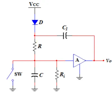
An intriguing type of ramp generator applies positive feedback to extend the range of linear operation with a constant current flow through a capacitor is shown in Figure 1 [1]. The switch in this circuit periodically closes to discharge the capacitor momentarily and initiate the capacitor charging cycle. The capacitor voltage would rise linearly if the charging current was constant. This would be so if, for example, a fixed voltage was applied across the resistor . But then the voltage at the upper end of the
Manuscript received on July 06, 2014; revised on September 23, 2014. T. Y. Elganimi was a teaching assistant in Electrical and Electronic Engineering Department, University of Tripoli, Libya, and currently he is a master student in the Department of Electronics and Computer Science (ESC), University of Southampton, United Kingdom, (e-mail addresses: [email protected], [email protected]).
resistor would have to increase continuously since the voltage across the capacitor increases as the capacitor charges. The circuit illustrated in Figure 1 is an ingenious method for doing just that.
The amplifier A in this circuit is used to copy the voltage across the capacitor without loading the capacitor. The voltage across the resistor is , and because of the action of the amplifier A remains even as the capacitor charges. Momentarily, closing the switch discharges the capacitor and initiates the charging cycle.
[image:1.595.331.516.432.586.2]In this circuit, the resistor indicates to the input resistance for the amplifier A, while the capacitor known as the bootstrapping capacitor which has a much higher capacitance than how the capacitor has. The function of the capacitor as will be shown, is to maintain a constant voltage across the resistor , and thus maintain the charging current constant.
Fig. 1. Basic Bootstrap Ramp Generator Schematic.
To the extent that the voltage across is essentially constant, this capacitor acts as a sort of temporary battery. It is of course necessary to assure that the capacitor is appropriately charged to provide the equivalent of the battery voltage. It is not feasible to connect directly to the capacitor , since the voltage at the - node is connected with a diode. The resistance should be large so it does not significantly affect the timing for the charging, and it should be small so that recharging occurs quickly. These conflicting requirements are met by using the diode. The capacitor charges quickly to (minus the diode voltage drop) through the diode. Then as the voltage across rises, so also does the voltage at the base of the diode, and the diode becomes reverse biased.
Design and Analysis of a Bootstrap Ramp
Generator Circuit Based on a Bipolar Junction
Transistor (BJT) Differential Pair Amplifier
Taissir Y. Elganimi
With ideal components, a linear ramp will only be produced if the charging current through the resistor is maintained constant, (i.e., if the voltage across is constant).
Just before the switch is opened, the voltage drop across the capacitor is equal to the supply voltage (i.e.,
), the voltage across the capacitor is zero (i.e., 0) and the output voltage is also zero (i.e., 0). When the switch opens, the voltage across the capacitor and the output voltage ( ) start to rise and the diode is immediately reverse biased, the constant voltage supply
is hence isolated from the charging circuit. The charging current is hence can be expressed as:
1
Substituting for which is equal to the difference between the charging current and the current through the input resistance for the amplifier, it can be expressed as follows:
2
Hence, for a linear ramp, the current through the capacitor and the resistor must be constant (i.e., ⁄ ), so, it is required that:
3
So, the voltage gain for this amplifier is equal to the ratio of the output voltage to the voltage across the capacitor and can be expressed as follows:
1 4
II. THE PROPOSED CIRCUIT DESIGN
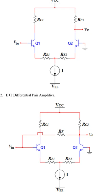
[image:2.595.346.508.135.328.2]The amplifier A in the circuit shown in Figure 1 can be an operational amplifier or a transistor as in [1]. The first stage of every operational amplifier is essentially a differential pair configuration which can be used in digital applications [2]. In this paper, it is proposed to be a bipolar junction transistor (BJT) differential pair amplifier as shown in Figure 2. This figure shows the basic BJT differential-pair configuration. It consists of two matched transistors and whose emitters are joined together and biased by a constant-current source , and each collector is connected to the positive supply voltage through a resistance . It is essential though that the collector circuits be such that and never enter the saturation mode.
It is very important to connect the input with the output by a feedback resistor as shown in Figure 3 to implement the same function of the resistor in the basic bootstrap ramp generator shown in Figure 1.
The feedback resistor provides a feedback path in the differential amplifier pair, and this type of feedback is called shunt-feedback. The voltage gain ⁄ for this circuit will be negative; this means that the input node at the base of
[image:2.595.319.514.141.542.2]pulls a current. As a result, it is possible to use this circuit to generate a ramp voltage waveform by inserting a capacitor at the input, and a switch in parallel with an input voltage could be put to control the output waveform, then the bootstrap ramp generator circuit which proposed in this paper can be as shown below in Figure 4.
Fig. 2. BJT Differential Pair Amplifier.
Fig. 3. BJT Differential Pair Amplifier with feedback resistor.
[image:2.595.319.514.345.544.2] [image:2.595.320.521.574.760.2]It is noticeable that the feedback is positive, i.e., as the voltage across the capacitor rises, the feedback provided through the amplifier applies a voltage to further increase in the voltage. A connection of this sort is commonly called a 'bootstrap' connection after the tongue-in-cheek suggestion that people can lift themselves off the ground by pulling up on their own bootstraps.
[image:3.595.54.284.236.390.2]In the bootstrap ramp generator circuit designed in this paper, the switch can be provided by a transistor driven between saturation (low collector-emitter voltage, approximately zero volts) and cutoff (approximately an open-circuit) by a pulse voltage input as shown below in Figure 5. The base resistor is used to limit the base current to safe values.
Fig. 5. Bootstrap Ramp Generator Using Differential Amplifier with a transistor acts as a switch.
The current source I can be constructed by a transistor driven in the active region to be as a constant current source.
III. THEORETICAL DESIGN
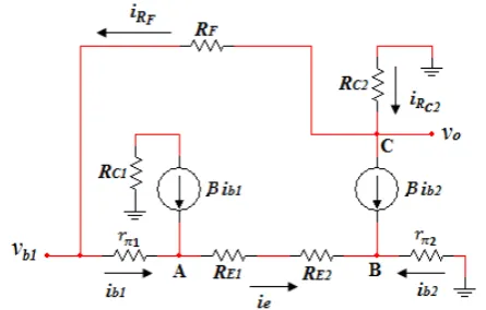
[image:3.595.58.281.577.719.2]It is important to analyze the designed circuit to derive the voltage gain for it and the equations which determine the relationship between the resistors in the designed circuit. The small-signal equivalent circuit (without the capacitor ) for the bootstrap ramp generator which designed in this paper can be shown as in Figure 6.
Fig. 6. The small-signal equivalent circuit for the designed circuit when the switch is closed.
Applying Kirchhoff Current Low (KCL) at point A gives the following equation:
5
And applying KCL at point B gives the following equation:
0 6
Substituting (5) in (6) yields:
7
The output voltage can be found at point C to be as follows:
8
The input voltage at the base of transistor can be expressed as follows:
1 9
So, the input resistance of this circuit (at the base of transistor ) can be found as follows:
∴ 1 10
Similarly, applying KCL at point C gives the following equation:
11
And also it is clear that:
12
Hence, the voltage gain can be expressed as follows:
1 1 13
This expression is the voltage gain for the designed circuit which is similar to that for the circuit in Figure 1.
Since the voltage gain must be greater than 1, then
1 1 14
Which results in the following condition for :
15
So, the feedback resistor must be in the range of for a precisely linear sweep to be obtained.
IV. CIRCUIT OPERATION
consider the dc voltage levels before, transistor is in the active mode, and the switch which provided by a transistor is in the cutoff mode before the input signal is applied. In general, the transistor is driven between saturation and cutoff by a pulse input voltage. When the switch is closed (at 0) by a positive-going input pulse, the transistor is saturated and the voltage across the capacitor is nearly
which can be approximated to be zero and its voltage is typically 0.2 V, and both and are in the active mode. Then, the output voltage is constant, and it can be expressed as follows:
0
2 16
And the constant current through the feedback resistor can be expressed as follows:
2 2 2 2 17
When the switch is open (at ), the voltage across the capacitor (i.e., the voltage across the base of ) increases linearly. So that, the voltage across the capacitor can be expressed as follows:
0 0 18
Where 0 is the initial value of the voltage across the capacitor at (0 ).
This means that transistor will try to increase its current level and hence lift the voltage present at its emitter. However, as it does this, the base-emitter voltage of will fall. Since the current in a bipolar transistor depends upon its base-emitter voltage, the result is that the emitter current of rises, and the emitter current of falls. The summation of these currents does not alter very much, but the balance between the two transistor currents and voltages changes. The result is that the rise in the voltage across the capacitor causes more current to flow through the collector of and less through the collector of . The reduction in the emitter current of means that it enters the cutoff region.
On the other hand, the voltage across the capacitor reaches a value higher than the voltage at the base of (which is grounded 0), and it will be in the range of
100 to 200 , it is greater than four times of the thermal voltage (i.e., 4 ), where is the thermal voltage which equals to 26 at room temperature. This means that the transistor is in the active mode and the transistor is in the cutoff. So, the switch is provided by a transistor driven between saturation and cutoff, and the transistor will be in the cutoff mode just the switch is opened.
In this case, the output voltage can be expressed as follows:
0 0 19
The output voltage at can be found as:
0 20
If the switch is turned ON (at ), the capacitor discharges rapidly and the transistor saturates, and both the voltage across the capacitor and the output voltage drop to its initial level. The time required for the output voltage to return to its initial value is called retrace time, and it can be derived to be as follows:
21
It is important to note that the sweep time is too long compared to retrace time , and the circuit now is ready to generate another output ramp.
In addition to producing a very linear output ramp, another advantage of the bootstrap generator is that the amplitude of the ramp can approach the level of the supply voltage .
V. DESIGNED EXAMPLE
In order to demonstrate the validity of the theory developed in this paper, a BJT differential pair amplifier was proposed to produce a linear voltage ramp waveform. The selected 2N1711 transistors had ( 230). And 1 current source is used. We also selected 2 ,
7.5 , 10 , and the supply voltage
25 .
The switch is provided by a transistor driven between saturation (low collector-emitter voltage approximating zero volts) and cutoff (approximating an open-circuit) with a pulse voltage input. The base resistor which used to limit the base current to safe values is chosen to be 1 . Switching is done by a 0.1 millisecond pulse with a 1 millisecond period.
The resistor for and can be calculated as follows:
1 22
Where is the emitter current for each transistor, and can be approximated as 0.5 . Then
12.012 Ω. From (10), the input resistance can be calculated to be equal to 948.024 Ω. So, the feedback resistor can be calculated according to equation (15) to be
769.476 to achieve a precisely linear sweep.
The output voltage when the switch is closed is calculated from (16) as 21.044 , and the constant current is calculated from (17) as 27.34 μ .
When the switch is opened at 0.1 , the voltage across the capacitor increases linearly and reaches at
VI. SIMULATION RESULTS
[image:5.595.50.291.137.328.2]In this paper, the proposed bootstrap ramp generator circuit designed in previous section was simulated using MULTISIM 11. Figure 7 shown below illustrates the input signal and the voltage waveform across both the capacitor and the output node.
Fig. 7. (a) The Input Voltage Waveform, (b) The Voltage Waveform across the Capacitor, (c) The Output Voltage Waveform.
The calculated and simulated values of the voltages show a good agreement between the values, which confirmed the theory validity. In contrast, there is a deferent result in the output voltage at 1 results from the nonlinearity sources. The nonlinearity results from the base current of
. As the capacitor voltage grows, the current increases. Since is part of the current , the capacitor charging current decreases slightly as increases. Thus, the charging current does not remain perfectly constant, and consequently, the ramp is not perfectly linear. Another source of nonlinearity is the emitter currents of the BJT differential pair amplifier which assumed to be equal when both and are in active mode.
A closer attention should be paid to the preceding reasoning about ramp linearity assumes that there is no significant leakage current through the capacitor. This requires that the capacitors should not be electrolytic.
VII. CONCLUSION
A proposal to design a bootstrap ramp generator circuit based on BJT differential pair amplifier is designed and presented in this paper. An analysis of the designed bootstrap ramp generator circuit is also discussed and simulated using MULTISIM 11. The results showed that there are some nonlinearity as a result of the base current of
and the emitter currents of the BJT differential pair amplifier. However, it is clear that the retrace time is far smaller than the sweep time. It is also obvious that the ramp can approach the level of the supply voltage in the designed circuit in this paper.
ACKNOWLEDGMENT
The author is highly indebted to all his family members for their continuous kind co-operation and understanding. He hopes to have other publications which might be better than this paper to dedicate to them in the near future.
REFERENCES
[1] Jacob Millman and Herbert Taub, Pulse Digital and Switching Waveforms. Tata McGraw-Hill, 1965.
[2] Adel S. Sedra and Kenneth C. Smith, Microelectronic Circuits, 5th ed,
Oxford 2004.