General approach to the analysis of plasmonic structures using spectroscopic ellipsometry
R. Verre,1,2,*M. Modreanu,3O. Ualibek,1D. Fox,1K. Fleischer,4C. Smith,1H. Zhang,1M. Pemble,3 J. F. McGilp,4and I. V. Shvets1,4
1Centre for Research on Adaptive Nanostructures and Nanodevices (CRANN) and School of Physics, Trinity College Dublin, Dublin 2, Ireland
2Department of Applied Physics, Chalmers University of Technology, 412 96 G¨oteborg, Sweden 3Tyndall National Institute, University College Cork, Lee Maltings, Dyke Parade, Cork, Ireland
4School of Physics, Trinity College Dublin, Dublin 2, Ireland
(Received 7 March 2013; published 24 June 2013)
In this article a route to analyze the full optical response of plasmonic structures is developed. First, the simple case of an anisotropic thin plasmonic layer supported on a transparent substrate is analyzed by introducing a quantity named anisotropic surface excess function (ASEF). The spectral features are analyzed in terms of effective dielectric function, demonstrating a more direct relation with the plasmonic response of the layer. The formalism is then generalized using a transfer matrix method. The formalism developed is supported by experimental evidence obtained by measuring the response of anisotropic nanoparticle arrays grown at a glancing angle. The agreement between theory and experiment is clear, suggesting that SE can be conveniently employed to measure the spectroscopic response of plasmonic structures. It is also demonstrated that the figure of merit of the plasmonic resonance for refractive index sensing can be greatly improved, with optimized measurement configurations, using polarized spectroscopy.
DOI:10.1103/PhysRevB.87.235428 PACS number(s): 61.46.−w, 78.67.−n, 07.60.Fs
I. INTRODUCTION
The interaction between electromagnetic waves and free electrons in a low-dimensional metallic structure results in surface plasmon effects.1,2 These can be considered as the normal excitation modes of the systems and have been the subject of tremendous interest due to their application as biological sensors,3–6 enhancement effects,7–9 and solar cell applications.10–12 When a metal nanoparticle (NP) is excited the electrons are highly localized and decay rapidly within the structures, resulting in localized plasmon resonances (LPRs).
LPRs manifest themselves by strong absorption/reflection peaks whose positions depend on the shape, size, and aspect ratio of the NPs, on the property of the surrounding medium, and on the interaction between the NPs.13 Their behavior is usually analyzed using conventional spectroscopic methods in the far field, but recently their charge distribution has been also addressed using more specific characterization meth-ods such as cathodoluminescence,14,15 transmission electron microscopy,16 and electron energy loss spectroscopy.17 The main limitation of conventional absorption spectroscopies is it allows one to monitor only in-plane properties of the plasmonic structures due to the inherent difficulties in the measurement geometry. To overcome this problem spectroscopic ellipsom-etry (SE) can be utilized as it can analyze changes in the polarization state of a linearly polarized beam reflected at oblique angles of incidence.18,19SE analysis has been extended to magnetic20 or anisotropic samples21 using generalized ellipsometry. Scattering and depolarization properties of the samples can also be addressed and separated by normal specular reflection. However, SE spectra are difficult to analyze as the response of the whole system needs to be modeled and compared with experiment to analyze the properties of the samples investigated.18 For this reason, the number of studies of plasmonic structures using SE is still limited.22–27 Previously it was demonstrated by our group28that a quantity, named anisotropic surface excess function (ASEF), could be
extracted from the experiment and the response of ultrathin plasmonic layer (<10 nm) directly analyzed. The advantage of ASEF is that it depends only on the optical properties of the plasmonic layer, allowing the modeling of the nanocomposite layer alone.28,29However, the validity of this approach appears to be limited to very specific cases, namely uncapped, thin plasmonic layers.
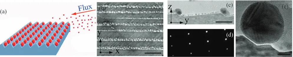
In this article a general approach based on a transfer matrix formalism has been developed. The method is general and can be adapted to multilayer structures, magnetically active, and anisotropic materials. The theory developed here is compared with measurements on samples produced using a self-assembled method based on a glancing angle deposition on a stepped template.30–33Adatoms are evaporated at shallow angles of just a few degrees onto a faceted c-plane Al2O3
surface. Parts of the surface are shadowed by the facets, resulting in adatoms being only deposited in exposed areas, spontaneously rearranging into NP arrays [see Fig.1(a)]. The technique is simple and large homogeneous areas covering the entire surface are realized. Furthermore, the technique has been shown to be largely independent of the deposited metal type as NP arrays of different materials have been produced using this method.34
(a) (b)
(c) (e)
(d)
FIG. 1. (Color online) (a) Schematic view of the deposition technique: A flux of collimated noble metal atoms is sent towards the surface at a glancing angle of incidence and coalesces on the step of a patterned surface, forming NP arrays. (b) Scanning electron micrograph of the Ag NP arrays deposited at a glancing angle of 6◦. Cross-section TEM images with low (c) and high magnification (e) are shown together with the axes as defined in the text. Rows of NP arrays are clearly visible along the step edge of the faceted template. The TEM micrographs were measured with a1010zone axis of the substrate [see diffraction pattern in (d)]. The scale bar in (b), (d), and (e) correspond to 200, 120, and 8 nm, respectively.
width of the plasmonic peak (). We will demonstrate that by changing from a normal incidence measurement to oblique angles, using polarization based optics, an increase in FoM of up to 5 times can be achieved for our structures. This could improve the detection limit of refractive index based sensors.36
II. EXPERIMENTAL METHODS
Noble metals NP arrays have been produced by glancing angle deposition on single crystalc-plane Al2O3 templates.
The substrates were off-cut 6◦ along the [1210] direction and polished on one side. To produce the faceted surfaces, a sample was annealed at 1400◦C in atmosphere for 16 h.37,38 AFM analysis confirmed the texturing of the template with a measured periodicity Ly =130 nm. The sample was then
loaded in a ultrahigh vacuum chamber (base pressure 2× 10⁻⁸ mbar) and Ag was deposited at a glancing angle of 6◦.
The nominal deposition rate, calibrated at normal incidence, was 2.8 nm/min and the sample was exposed for 30 min. The deposition was performed at room temperature.
Subsequently, the in-plane morphology was imaged by a field emission Carl Zeiss ULTRA scanning electron micro-scope (SEM). SE measurements were performed within a few hours of exposure of the sample to atmosphere using a Woollam M2000 variable angle spectroscopic ellipsometry system, equipped with a rotating compensator and a high speed CCD camera. The measurements were performed with a spectral range of 245–1600 nm. The sample was aligned at each angle of incidence and rotated manually around the surface normal (azimuthal rotationϕ). The estimated error in the accuracy of the rotation angle was established to be±5◦.
After these measurements, a Ag NP sample was capped with a 50 nm Si3N4 layer to facilitate TEM analysis. The
deposition was performed using a plasma enhanced chemical vapor deposition using 5% SiH4 and NH3 as precursors
(1:6 ratio).
In order to analyze the out-of-plane morphology of the Ag capped sample, TEM out-of-plane sections were prepared using a Carl Zeiss Auriga CrossBeam FIB-SEM. Once prepared, the section was imaged by a Titan TEM operating at 300 kV. The substrate was aligned to the 1010 zone
axis for imaging. In all cases the images were acquired in bright-field mode.
III. NANOPARTICLE GROWTH AND ASEF FORMALISM The SEM of the in-plane structure deposited at a glancing angle is shown in Fig. 1(b). The structure appears as a collection of ordered NP arrays aligned along the step edges as previously reported. The in-plane semiaxes (averageRx=12
nm andRy=10 nm) are well below the optical diffraction
limit and the plasmonic layer can therefore be considered as an homogeneous anisotropic layer with an effective dielectric functionεL. As the average center-to-center distance Lx is
27 nm, the interparticle separation (∼3 nm) is much smaller than the average NP diameter and a strong enhancement of the electric field is expected to take place in the interstitial space between NPs. In order to fully characterize the sample, the out-of-plane morphology has been also analyzed by TEM [see Figs. 1(c) and 1(e)], revealing the NPs appear as truncated ellipsoids of height H=17 nm. Details of the growth mechanism of such structures can be found elsewhere.35,39 In the following, the in-plane directions will be referred asx (along the NP rows) andy(perpendicular to the rows), while the out-of-plane direction will be defined asz(see sketch in Fig.2).
The response of the as-grown structures has been first analyzed by SE using a fixed angle of incidence =61◦, and by changing the azimuth of the sample in the plane of incidence by an angle ϕ [see sketch in Fig. 2(a)]. This incidence angle was chosen as it corresponds to the Brewster angle of the substrate. In this way, the difference between rp and rs is maximized and the response of the system
can be analyzed more accurately.28 Usually, ellipsometric observables are expressed in terms of the complex reflection ratioρ=rp/rs=tan ei. The elliptical polarized light after
[image:2.608.61.558.71.168.2](a) (c) (d)
(f) (e)
(b)
FIG. 2. (Color online) (a) Sketch for the SE measurement of Ag NP arrays in the parallel measurement configuration. The axis and angle definitions are also indicated. (b) Ellipsometric angles tan (solid line) and(dashed line) for the parallel and perpendicular configuration. Real (c) and imaginary (d) parts of the pseudodielectric functionε of Ag NP arrays grown at a glancing angle for different azimuthal angle rotationsϕand=61◦. The intensity of thexresonance at 2.2 eV follows aεL,xcos2ϕ+εL,ysin2ϕdependency [inset in (c)]. In
(e) and (f) experimental (dotted lines) and simulated (continuous) ASEF for the parallel (ϕ=0◦) and perpendicular (ϕ=90◦) measurement configurations are shown. The insets show the modeled plasmonic layer dielectric functionεLusing the parameters extracted from micrograph
analysis.
of the plasmonic NPs themselves. A simple solution for accessing the dielectric properties of the plasmonic features is achieved by defining the psuedo-(effective) dielectric function for the whole bulk system, which can be extracted from the raw measurements using18
ε =sin2+sin2tan2
1−ρ 1+ρ
2
. (1)
In this case, superimposed to the substrate dielectric function, resonances are clearly visible in Fig.2(c)for the real part of
ε, and the resonance position blues shifts upon increases of the azimuthal angle rotation (see inset).
Following previous studies of similar structures, a quantity, named anisotropic surface excess function (ASEF)28 has been extracted from the experiment to obtain quantitative information on the optical properties of the NP layer itself. The advantage of introducing the ASEF method relies on its simplicity as it depends only on the response of the plasmonic layer alone and can therefore be modeled using simple analytical or numerical methods.29,40 In particular, the plasmonic layer investigated here has been modeled as a collection of supported identical ellipsoids placed on a rectangular lattice, and interacting through dipolar forces. This method has been previously used to reproduce the anisotropic optical response of similar NP arrangements.28,35
The ASEF extracted from this experiment and modeled data are shown in Figs.2(e)and2(f). A semiquantitative agreement is clearly observable using values for average NP dimensions and separation obtained from SEM and TEM images. There is a clear correspondence between the measured ASEF and the modeled dielectric function of the layer, shown in the
inset in Figs. 2(e) and 2(f), highlighting the usefulness of this approach. For the parallel measurement configuration, the resonance at ∼2.2 eV is then referred to a resonance along the array (x resonance), while the minima at higher energy is attributed to a z resonance. The opposite sign in the out-of-plane z resonance is due to the discontinuity of the perpendicular component of the electric field in Maxwell boundary conditions.41 Once ϕ is increased, the resonance shifts towards the blue as the mode along the y direction, which resonates at a higher energy of∼2.9 eV, is also excited. The behavior can be quantitatively described by introducing a rotation matrix for the layer dielectric function. In this case the peak height is expected to follow aεL,xcos2ϕ+εL,ysin2ϕ.
The inset in Fig. 2(c) illustrates this trend for the 2.2 eV x-resonance intensity.
[image:3.608.55.556.70.300.2]IV. EXTENSION USING A TRANSFER MATRIX FORMALISM
In the previous section it was shown that the ASEF approach can be successfully applied to the analysis of plasmonic layers. However, the ASEF can only be used in case of a three phase system (substrate, plasmonic layer, and air), the nanocomposite layer is thin, the substrate response is isotropic, and the optical axes are aligned with the high symmetry axis of the system. In particular, the ASEF approach becomes inaccurate when multilayer structures or thick plasmonic layers are considered, rendering its application limited to very specific cases. The problem can be overcome, if the effective dielectric function of the NP layer is treated as an embedded layer in a full optical model using the transfer matrix approach. Originally formulated for isotropic media,42 it has been formulated in a more general fashion by Schubert.43,44 This method can be applied whenever the thickness and the dielectric function of each layer composing the system are known. Following this approach, a four vector is defined for the p and s components of the electric E and magnetic H field and each layer can be then defined by a 4×4 partial transfer matrix Tp. By knowing the dielectric properties of
each layer, the partial transfer matrix of each individual layer can be calculated and the full response of the system derived. In this way, an expression of the complex reflection coefficient can be obtained and compared to the experiment.
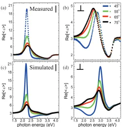
The validity of this approach is first tested on the same sam-ple for parallel and perpendicular configuration by comparing the simulations with spectra measured at different angles of incidence. As before, also in Fig. 3 resonances appear in the real part of the pseudodielectric functions. Compared to common bulk materials, the effective response of the system studied here strongly depends on the angle of incidence of the incoming light and reaches remarkably high values at the x-resonances energy. As the polarizability of a material is proportional to its dielectric function, a strong electric field displacement is hence expected within the NP layer, as for any plasmonic structure at resonance. The sample is however anisotropic, and the reflection coefficient depends also on the azimuthal angle. Excellent agreement between experiment and theory was found for both the real and imaginary component using an effective NP layer thicknessd =1.5 nm, confirming the formal equivalence of the previously discussed three layer model (ASEF) with the transfer matrix approach for our samples. For the perpendicular configuration [Figs.3(b) and3(d)], there is qualitative agreement in the y-resonance peak shift upon changes in angle of incidence, but peak positions and intensity are overestimated. The disagreement is attributed to the previously mentioned difference in measured and simulated y resonance position originating from an oversimplification in the dipolar model.
Of particular interest is the fact that, for the ϕ=0◦ measurement configuration [Fig. 3(a)] the intensity of the positive peak at 2.2 eV increases by a factor of ∼5 when going from=70◦to=45◦, increasing the signal to noise ratio. At the same time the resonance sharpens, resulting in an increase in its figure of merit (FoM) by a factor of ∼3. In case of anisotropic samples, the possibility of measuring such sharp resonances could be of great interest, as its FoM is
(a) (b)
(c) (d)
FIG. 3. (Color online) Real part of the pseudodielectric func-tion for (a) the measurement configurafunc-tion parallel ,ϕ=0◦ and (b) perpendicular⊥,ϕ=90◦ to the array, for different angles of incidence. The simulated pseudodielectric functions for the two cases calculated using the transfer matrix formalism are shown in (c) and (d), respectively.
greatly increased. These effects are well reproduced by the simulation, which also suggest that the FoM can be even further increased at a measurement angle of∼35◦, a possibility that instrumental limitations did not allow us to explore. These results suggest that the sensitivity of refractive index plasmon-based biosensors can be increased significantly by choosing an appropriate angle of incidence and measuring polarized reflectance ratios.
(a) (b)
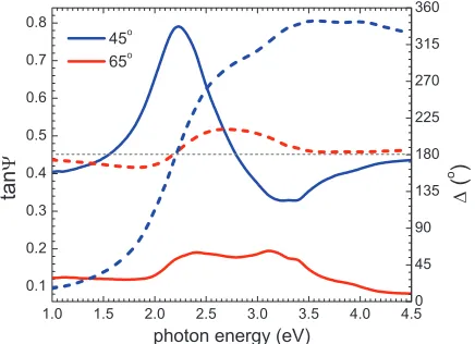
[image:4.608.311.561.66.326.2] [image:4.608.313.560.530.669.2]FIG. 5. (Color online) Simulation of the ellipsometric angles at =65◦ and=45◦. At the 2.2 eV resonance a=180◦phase shift occurs upon reflection. At the same time, for the 45◦incidence angle, the amplitude ratio tan reaches values close to one, hence explaining the increase in the intensity of the resonance observed in Fig.3.
As a representative example, in Fig. 4 a comparison is shown between the simulated absorption and SE spectra when the NP arrays are surrounded by different dielectric media. The absorption profiles were obtained using the relation Aabs,x∝Im[εL,x]/λ.45 As expected, an increase in
the refractive index surrounding the NPs redshifts the x resonances. However, a much sharper profile is obtained for the pseudodielectric function, leading to a narrowing of the peak of∼5. Similar enhancements have been recently reported for in-plane symmetric systems when measuring the phase difference between the p- ands-polarized components as a function of the incidence angle.25 It is clear that measuring relative changes in p- and s-polarized reflection, using an optimised measurement configuration, offers the possibility of significant improvement in the FoM of plasmonic sensors. Phase sensitive measurements appear then as a sensitive route which can lead to single molecule recognition, as recently discussed.46
To understand the origin of the observed changes in the pseudodielectric function intensity, the simulated tan and have been plotted in Fig.5for two angle of incidence (=65◦ and=45◦). It can be noticed that at resonance a 180◦phase difference betweenrpandrsoccurs for both angle of incidence.
However, at a shallower angle of incidence, the complex ratio amplitude tan reaches larger values as the intensity of the p- ands-polarized reflection is comparable. In this way, the denominator in Eq. (1) approaches zero and a singularity appears for the overall system response. Sharper and more intense resonances can be measured whenever the intensity of the reflection coefficients are comparable and at the same time a phase retardation ofπtakes place. This is a general condition which can be verified for different anisotropic systems.
The transfer formalism can be also adapted to other opti-cal characterization methods, such as reflectance anisotropy spectroscopy39 and different materials. The theory could be extended to magnetically active systems44and core-shell plas-monic structures,47 and a complete analysis on the behavior of each reflection coefficient becomes possible. This more
general approach appears to be a more suitable and convenient method to simulate and analyze the spectroscopic response of plasmonic structures, even included within multilayer structures.
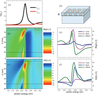
In the following, the effect of increasing the NP layer thickness is finally addressed, while the NP size and distri-bution on the substrate remains fixed. As previously pointed out, simulations using transfer matrix require a given optical thickness for each layer composing the stack. For inhomoge-neous plasmonic layer as the one here investigated, its effective thickness is not equivalent to the NP height. During previous simulations, a thickness of 1.5 nm was considered, in line with the nominal deposited Ag thickness for the system of 1.3 nm. While this is a crude estimation it resulted in amplitudes comparable to those measured in the experiment.
Figure 6 shows the simulated SE spectra for increasing layer thickness d. To simplify the analysis, the plasmonic layer was assumed to be in-plane isotropic (Rx=Ry=20
nm andRz=7.5 nm), and with an Ag particles spacing large
enough to disregard any interparticle coupling (N=7×10¹³
N P/m2). The self-image charge produced by the substrate is
still taken into account. With these parameters, the dielectric function of the layer is shown in Fig.6(a). As the sample is in-plane isotropic,ε is now independent of the azimuthal rotation angleϕ. Figures6(b)and6(c)show that changes in the plasmonic film thickness result in a strong modification of the SE response.
In particular, it can be noticed that for ultrathin structures, the plasmonic resonances appear in Re[ε] and its imaginary part assumes unphysical negative values. These changes are related to the presence of the plasmonic layer, which heavily modifies the polarization properties of the reflected beam as also shown in the experiment in Fig.2. This phenomena are characteristic for ultrathin layers, as it can be shown that Re[ε]∝Im[εL].29In particular, this proportionality relation
is valid whenever the plasmonic film is thin, i.e.,28
d λ
4πεL,j −sin2θ
. (2)
Figure6now allows a more precise quantification of Eq.(2): Even for an effective plasmonic layer of 5 nm a mixture between the layer and effective dielectric functions takes place and the simple proportionality is no longer valid. It would be then of great interest to understand how the NP height affects the effective plasmonic layer thickness. This possibility cannot be easily investigated using the glancing angle deposition method described here as the NP produced are usually smaller than 20 nm. However, it appears that large layer thickness results in an even more complex behavior that is difficult to relate directly to the plasmonic features, but can be addressed easily using the transfer matrix approach.
During the simulation throughout the text, the anisotropy of the substrate has been disregarded. Even though Al2O3is a
[image:5.608.65.283.71.229.2](a)
(b)
(c) (f)
(e) (d)
FIG. 6. (Color online) (a) Simulated imaginary part of the dielectric function of supported isotropic spheroids along thexandzdirection. The contour plot of the real and imaginary part of the calculated psuedodielectric function for different plasmonic layer thicknessd[see sketch in (d)] are shown in (b) and (c), respectively. The vertical dotted line shows the position of thexresonance and it is used as a guideline. For clarity, in (e) and (f) the real and imaginary part of the dielectric function for different thicknessdare also shown.
The SE response originated by plasmonic structures de-pends on many contributing factors, such as NP morphologies, material composition, and substrate dielectric function. The overall response can be heavily modified by changes in any of them. In particular, it has to be noted that the discussion of the FoM by directly using the pseudodielectric function is another simplification allowed by the use of a transparent substrate. Once nontransparent substrates are used the dielectric properties of the NP layers have to be extracted by optical models, as it is standard practice in ellipsometric analysis. Using the general approach described here, the unknown parameters can be treated as fitting parameters and the modeling refined using the standard ellipsometric approach to multilayer structures.18 In this case, clearly, analytical models for the NP dielectric function, as used here, are much more suited for fast convergence.
V. CONCLUSIONS
We have demonstrated and developed a methodology to investigate the spectral response of complex plasmonic
material systems. Simulations were compared with the re-sponse of anisotropic NP arrays grown at glancing angles and measured using SE. First, the anisotropic surface excess func-tion (ASEF) was introduced and it was shown how the plas-monic response of layer can be directly extracted. The formal-ism is further generalized utilizing a transfer matrix method. Different effects that can lead to a modification in the response of the system were discussed and the methodology for a complete analysis outlined. The approach can be used for thick NP layers, anisotropic systems, and different materials, and can be extended to magnetic systems and core-shell structures.47
[image:6.608.112.503.69.442.2]ACKNOWLEDGMENTS
This work has been funded by Science Foundation of Ire-land, Contract No. 06/IN.1/I91 and 11/RFP.1/PHY/3047 and conducted under the framework of the INSPIRE programme,
funded by the Irish Government’s Programme for Research in Third Level Institutions, Cycle 4, National Development Plan 2007–2013. O. Ualibek would like to thank the Government of Rep. of Kazakhstan under the Bolashak programme.
1U. Kreibig and M. Vollmer,Optical Properties of Metal Clusters (Springer, Berlin, 1957).
2L. Brongersma and P. Kik, Surface Plasmon Nanophotonics (Springer, Berlin, 2007).
3K. A. Willets and R. P. Van Duyne,Annu. Rev. Phys. Chem.58,
267 (2007).
4J. Homola,Chem. Rev.108, 462 (2008).
5F. Hao, Y. Sonnefraud, P. Van Dorpe, S. A. Maier, N. J. Halas, and P. Nordlander,Nano Lett.8, 3983 (2008).
6N. Verellen, P. Van Dorpe, C. Huang, K. Lodewijks, G. A. E. Vandenbosch, L. Lagae, and V. V. Moshchalkov,Nano Lett.11, 391 (2011).
7S. Nie and S. R. Emory,Science275, 1102 (1997).
8S. Kim, J. Jin, Y.-J. Kim, I.-Y. Park, Y. Kim, and S.-W. Kim,Nature
(London)453, 757 (2008).
9A. Kinkhabwala, Z. Yu, S. Fan, Y. Avlasevich, K. Mullen, and W. E. Moerner,Nat. Photon.3, 654 (2009).
10H. Atawer and A. Polman,Nat. Mater.9, 205 (2010).
11R. A. Pala, J. White, E. Barnard, J. Liu, and M. L. Brongersma,
Adv. Mater.21, 3504 (2009).
12J. N. Munday and H. A. Atwater,Nano Lett.11, 2195 (2011). 13H. Lance and E. Coronado, J. Phys. Chem. B107, 668 (2003). 14R. Gomez-Medina, N. Yamamoto, M. Nakano, and F. J. G. de
Abajo,New J. Phys.10, 105009 (2008).
15E. J. R. Vesseur, F. J. Garcia de Abajo, and A. Polman,Nano Lett. 9, 3147 (2009).
16J. A. Scholl, A. L. Koh, and J. A. Dionne,Nature (London)483,
421 (2012).
17J. Nelayah, M. Kociak, O. Stephan, F. J. Garcia de Abajo, M. Tence, L. Henrard, D. Taverna, I. Pastoriza-Santos, L. M. Liz-Marzan, and C. Colliex,Nat. Phys.3, 348 (2007).
18R. Azzam and N. Bashara,Ellipsometry and Polarized Light(North Holland, Amsterdam, 1977).
19M. Losurdo, M. Bergmair, G. Bruno, D. Cattelan, C. Cobet, A. de Martino, K. Fleischer, Z. Dohcevic-Mitrovic, N. Esser, M. Galliet, R. Gajic, D. Hemzal, K. Hingerl, J. Humlicek, R. Ossikovski, Z. Popovic, and O. Saxl,J. Nanopart. Res.11, 1521 (2009).
20K. Mok, N. Du, and H. Schmidt,Rev. Sci. Instrum.82, 033112
(2011).
21Y. Lo, W. Hsieh, Y. Chung, and S. Tsai,J. Lightwave Technol.30,
2299 (2012).
22P. C. Wu, T.-H. Kim, A. S. Brown, M. Losurdo, G. Bruno, and H. O. Everitt, Appl. Phys. Lett.90, 103119 (2007).
23J. M. Flores-Camacho, L. D. Sun, N. Saucedo-Zeni, G. Weidlinger, M. Hohage, and P. Zeppenfeld,Phys. Rev. B78, 075416 (2008).
24P. C. Wu, M. Losurdo, T.-H. Kim, B. Garcia-Cueto, F. Moreno, G. Bruno, and A. S. Brown,J. Phys. Chem. C115, 13571 (2011).
25K. Lodewijks, W. Van Roy, G. Borghs, L. Lagae, and P. Van Dorpe,
Nano Lett.12, 1655 (2012).
26S. Zhu, T. Chen, Y. C. Liu, Y. Liu, and S. F. Yu, Electrochem.
Solid-State Lett.15, k5 (2012).
27V. G. Kravets, F. Schedin, A. V. Kabashin, and A. N. Grigorenko,
Opt. Lett.35, 956 (2010).
28R. Verre, K. Fleischer, C. Smith, N. McAlinden, J. F. McGilp, and I. V. Shvets,Phys. Rev. B84, 085440 (2011).
29M. Kelly, S. Zollner, and M. Cardona, Surf. Sci. 285, 282
(1993).
30A. Sugawara, G. Hembree, and M. R. Scheinfein,J. Appl. Phys.82,
5662 (1997).
31T. Oates, A. Keller, S. Facsko, and A. Micklich,Plasmonics2, 47
(2007).
32F. Cuccureddu, S. Murphy, I. Shvets, M. Porcu, and H. W. Zandbergen,Nano Lett.8, 3248 (2008).
33R. Verre, K. Fleischer, R. G. S. Sofin, N. McAlinden, J. F. McGilp, and I. V. Shvets,Phys. Rev. B83, 125432 (2011).
34R. Verre, K. Fleischer, O. Ualibek, and I. V. Shvets,Appl. Phys.
Lett.100, 031102 (2012).
35R. Verre, K. Fleischer, J. F. McGilp, D. Fox, G. Behan, H. Zhang, and I. V. Shvets,Nanotech.23, 035606 (2012).
36J. R. Sambles, G. W. Bradbery, and F. Yang,Cont. Phys.32, 173
(1991).
37J. R. Heffelfinger, M. W. Bench, and C. B. Carter,Surf. Sci.370,
168 (1997).
38R. Verre, R. Sofin, V. Usov, K. Fleischer, D. Fox, G. Behan, H. Zhang, and I. Shvets,Surf. Sci.606, 1815 (2012).
39O. Ualibek, R. Verre, B. Bulfin, V. Usov, K. Fleischer, J. McGilp, and I. V. Shvets,Nanoscale5, 4923 (2013).
40W. Plieth and K. Naegele,Surf. Sci.64, 484 (1977).
41T. Yamaguchi, S. Yoshida, and A. Kinbara,Thin Solid Films18, 63
(1973).
42M. Born and E. Wolf,Principles of Optics(Cambridge University Press, Cambridge, 1999).
43M. Schubert,Phys. Rev. B53, 4265 (1996).
44M. Schubert, T. E. Tiwald, and J. A. Woollam,Appl. Opt.38, 177
(1999).
45C. Bohren and D. Huffman,Absorption and Scattering of Light by
Small Particles(Wiley, New York, 1983).
46V. G. Kravets, F. Schedin, R. Jalil, L. Britnell, R. V. Gorbachev, D. Ansell, B. Thackray, K. S. Novoselov, A. K. Geim, and A. N. Grigorenko,Nat. Mater.12, 304 (2013).