3-Dimensional inkjet printing of macro structures from
silver nanoparticles
Jayasheelan Vaithilingam
a,⁎
, Ehab Saleh
a, Lars Körner
a,b, Ricky D. Wildman
a, Richard J.M. Hague
a,
Richard K. Leach
b, Christopher J. Tuck
aa
Centre for Additive Manufacturing, The University of Nottingham, Nottingham NG7 2RD, UK b
Manufacturing Metrology Team, Faculty of Engineering, The University of Nottingham, Nottingham NG7 2RD, UK
H I G H L I G H T S
• 3-dimensional structures were inkjet printed using silver nanoparticles in a single-step.
•The voids witnessed in the 600 dpi sam-ple are primarily due to insufficient merging of the ink droplets.
•Residual surface temperature due to in-frared exposure for sintering caused pinning and limited the droplets to merge.
•By increasing the printing resolution to 750 dpi, the merging of droplets was improved.
•750 dpi sample showcased reduced void percentage and improved hardness compared to 600 dpi sample.
G R A P H I C A L A B S T R A C T
a b s t r a c t
a r t i c l e i n f o
Article history: Received 31 January 2017
Received in revised form 25 September 2017 Accepted 27 October 2017
Available online 31 October 2017
The adoption of additive manufacturing technology is gaining interest for processing precious metals. In this study, the capability of inkjet printing was explored to fabricate macroscopic parts from commercial silver nano-particle ink (AgNPs). A bespoke JETx® three dimensional (3D) inkjet printing machine was used to print and sub-sequently sinter up to 1000 layers of AgNPs using an infrared source. Examination of the sample using X-ray computed tomography and scanning electron microscopy revealed the existence of both micro- and nano-scale pores within the structure. Pinning effect, residual surface temperature, insufficient droplet overlap and sur-face defects were the key factors contributing to the voids. Elemental mapping confirmed the structure to be composed of 87% of silver along with carbon and oxygen. The 750 dpi sample showed a 25% reduction in nanopores and 77% lower micro-pores compared to the 600 dpi sample. In terms of hardness, the 750 dpi sample was 29% harder than the 600 dpi sample, showcasing samples with higher print resolution can contribute to-wards less voids and improved mechanical properties. Thus by demonstrating the possibility to fabricate dense parts from AgNPs using inkjet technology, this study opens a novel route for processing nano-scale particulates and precious metals in 3D.
© 2017 The Authors. Published by Elsevier Ltd. This is an open access article under the CC BY license (http:// creativecommons.org/licenses/by/4.0/). Keywords:
Additive manufacturing 3D–printing Silver nanoparticles Inkjet printing Precious metals
⁎ Corresponding author at: Centre for Additive Manufacturing, Coates Building, Faculty of Engineering, The University of Nottingham, University Park, Nottingham, NG9 7RD, UK. E-mail address:[email protected](J. Vaithilingam).
https://doi.org/10.1016/j.matdes.2017.10.070
0264-1275/© 2017 The Authors. Published by Elsevier Ltd. This is an open access article under the CC BY license (http://creativecommons.org/licenses/by/4.0/). Contents lists available atScienceDirect
Materials and Design
1. Introduction
The success of additive manufacturing (AM) infinding a place in mainstream manufacturing is primarily dictated by the added advan-tages of AM compared to the traditional forming and subtractive methods. Some of the key advantages of this computer aided design (CAD) driven process include, but are not limited to, (i) freedom of de-sign (ii) the ability to produce near-net shape and end use parts, (iii) re-duced time-to-market, (iv) decreased supply-chain, (v) reduced post-processing requirements in terms of tooling, (vi) high material utilisation rate and (vii) less wastage[1]. Among the seven AM process-es classified by the American Society for Testing and Materials (ASTM), VAT photo-polymerisation, material jetting (MJ), material extrusion, powder-bed fusion (PBF) and directed-energy deposition (DED) are the most common. Among these, PBF and DED are the most widely used methods for processing metals.
With recent advancements in material development, PBF technolo-gies, including selective laser melting (SLM), direct metal laser sintering (DMLS) and electron beam melting (EBM), are used to fabricate parts for various automotive, aerospace and biomedical applications. Al-though a wide range of metals and alloys can be processed using this technology, studies processing precious metals such as gold (Au), silver (Ag), platinum (Pt) and their alloys are limited[2]. There is a growing interest in the jewelry industries to use these computer driven process-es to make customised products with a high degree of precision and ac-curacy[3,4]. Hence, AM is considered as one of the key enablers for processing precious metals.
Khan and Dickens[31]showcased the ability to process 24 carat Au using an SLM machine[5]. However, the high reflectance (85%) of the Au particles near the infrared range was observed to affect the energy absorption during laser processing, leading to poor interlayer adhesion with 12% to 15% porosity. In addition to reflectance, the thermal conduc-tivity of Au, balling of the metals during laser scanning and spreading of the melt pool were observed to affect the SLM process[5]. SLM fabrica-tion of dental crowns reported previously showcased a rough surface texture with inferior mechanical properties such as hardness (28 HV) and modulus (72.5 GPa)[6]. Hence in order to improve the processabil-ity of precious metals and improve the densprocessabil-ity of the fabricated parts, they are alloyed with other metals, such as silver, copper, silicon and germanium, for the jewelry applications[7,8].
Though alloying the metals may improve the SLM fabricated part's characteristics, alloying of a metal purely for processing in a particular equipment is undesirable at the expense of purity and the inherent properties of the metal. For example, the high electrical conductivity of gold may be compromised by the addition of other metals. Moreover, processing high volumes of these metals through an SLM process may add more constraints economically. With the advent of Precious M 080 by the AM machine manufacturer EOS, alloying the precious metals for SLM processing, attaining dense parts, recovering the material spread on the build platform and re-using them for future builds is no longer a problem. However, printing multiple material parts using the available PBF methods is still challenging–both technically and eco-nomically. Hence, the use of PBF for processing precious metals is less attractive.
Current research in AM has high interest in processing multiple ma-terials to enable multi-functionality[9]. Although several AM processes, such as extrusion and MJ, have showcased fabrication of multi-material parts, it is difficult to achieve with PBF[10]. This is mainly due to the fact that separation of materials after fabrication for reuse could be problem-atic due to contamination of the materials.
Despite these challenges with metal AM, printing conductive tracks for electronics applications using inks containing metalflakes and metal nanoparticles (MNPs) is increasing[11]. However, in recent years, the use of inkjet (IJ) systems (a MJ technology) for printing MNPs forfl exi-ble electronics applications is extensive[12–17]. Inkjet, being a drop-on-demand (DOD) printing system, it is capable of printing at high
resolution, with less material wastage. The advantage of inkjet printing has been well documented in the literature[18]. Much of the previous research concentrated on using MNPs to print circuits for electronics ap-plications and most of them are limited to a few layers (b20)[19–21]. A recent study has documented combined printing and sintering of 50 layers of silver nanoparticles (AgNPs) towards enabling multifunctional AM (MFAM) for electronics application[22]. In concert, a recent innova-tion in system architecture has been shown by XJet®, whereby an inkjet based printing machine has been developed to produce metallic parts from nanoparticles[23]. The system is capable of processing a structural material and a supporting material; however, multi-material printing is limited. Microstructure, surface and mechanical properties of the parts produced by XJet® remains unknown. An understanding on the evolu-tion of the microstructure is essential in order to build 3D structures with optimal mechanical properties. Whereas, the existing knowledge of microstructure of sintered nanoparticles for multiple layers (N100 layers) is limited.
In order to further the existing knowledge and to assess the ability of IJ printing to produce macro structures from nanoparticles, a study on printing and subsequently sintering of multiple layers of metal-nanoparticles and characterising the printed structures for porosity and mechanical stability would be beneficial. To address this, the poten-tial of IJ printing to fabricate macro-structures from MNP inks has been evaluated in this study by printing and subsequently in-process sintering multiple layers of AgNPs using a bespoke JETx® 3D multi-material IJ printing machine. This in-process sintering mechanism can significantly save time and effort required to build multiple layers, and improve the process efficiency. The micro-structure, surface chemical analysis, porosity and hardness of the printed silver samples have been reported.
2. Materials and methods
2.1. Materials
An ink containing AgNPs (~ 30–35 wt%) was purchased from Ad-vanced Nano Products, South Korea. Alumina substrates were pur-chased from Ceramic Substrates and Components Ltd., UK. Pre-cleaned borosilicate glass slides were purchased from Cole-Palmer®, UK. Kapton® tape was supplied by RS Components, UK and EpoFix® cold mount resin and hardener kit was obtained from Struers®, UK. Silicon carbide grinding pads and diamond pastes for polishing were supplied by Buehler®, UK. Acetone and 2- propanol for cleaning were obtained from Sigma Aldrich, UK.
2.2. Methods
2.2.1. Design
A 3 mm × 3 mm square pattern with 600 dots per inch (DPI) and 750 dpi was designed using an open source GNU Image Manipu-lation Program (GIMP). This design was replicated to make four 3 mm × 3 mm patterns in a 15 mm × 9 mm canvas and the image was saved as a bitmapfile (.bmp). GIMP was used to design the dem-onstrators with a print resolution of 500 dpi.
2.2.2. Substrate preparation
Alumina substrates were used for printing the silver patterns. These alumina substrates were sonicated for 5 min using acetone and 2-propanol and placed on a glass slide. The alumina substrates were placed on the centre of a glass slide and the edges of the substrates were attached to the glass slide using Kapton® tape to prevent move-ment while printing.
2.2.3. 3D inkjet printing
print heads. The machine is built for the substrate/build platform to move in X axis and the print head in Y and Z axis. The substrate moves to the‘print station’and droplets of ink were ejected based on the supplied bitmap pattern. Once a layer was printed, the substrate then moved under the IR source to sinter the AgNPs. After passing the sample under IR for a predefined number of passes, the substrate moved back to the print station to print the next layer. After printing a layer, the print head moved in the Z direction to a predefined layer thickness and repeated the printing step. These steps were repeated until the required number of layers were completed; following printing, the silver samples were removed from the ceramic substrate by gently pushing it away from the substrate using theflat end of a glass slide. The removal of the samples was easy due to weak adhesion of the silver samples to the ceramic substrates; however, the sample neither moved during printing, nor was damaged during the removal process. The sam-ples removed from the ceramic substrates were then characterised. Table 1shows the process parameters used for printing and sintering of AgNPs. Further details on the printing machine and the procedure can be obtained from the literature[22]. Printing and sintering condi-tions specified for 600 dpi were used to build demonstrators.
2.2.4. Characterisation
2.2.4.1. Surface morphology.A Nikon Eclipse (LV100ND) optical micro-scope was used to obtain the surface morphology of the printed sam-ples. Built-in software (NIS) was used to obtain the images and measure the size of the printed tracks.
2.2.4.2. Scanning electron microscopy.A scanning electron microscope (SEM)fitted with afield emission gun (FEG SEM; JOEL7100F) was used to obtain the microstructural features of the printed patterns. An electron back-scattered detector (EBSD) was used to image the sample with an acceleration voltage of 10 kV and a working distance of 10 mm. For SEM characterisation, the printed samples were cold-mounted using an epoxy resin and ground carefully using P800 and P1200 grits. These samples were then polished using a pad containing 6μm and 1 μm diamond paste. The polished sample was then sputter coated with platinum for 90 s to make the sample conductive. Hot press mount was not used in this study since the mounting temperature can change the microstructure of the printed samples.
2.2.4.3. Elemental analysis.Elemental composition of the printed samples was obtained using an energy dispersive X-ray (EDX) spectrometer fitted to the Hitachi 3030 SEM. The SEM was operated in the EDX mode. A spot diameter of 10μm was used to probe the sample in three arbitrary areas and elements were assigned based on the peak po-sition. Surface elemental mapping was performed using Quantax 70 (Bruker Nano GmbH).
2.2.4.4. Porosity.A MCT 225 Nikon X-ray computed tomography (XCT) system was used to acquire the projection data set[24]. The XCT system has a temperature controlled scan chamber of 20 °C ± 0.5 °C and the manufacturers stated maximum permissible error is stated asð9þ L
50Þ μm, whereLis the length of the measurement in millimetres. The accel-eration voltage of the electron beam was set to 225 kV, with a current of
14μA. The source of the XCT system has a cooled reflection tungsten tar-get. Afilter of 0.85 mm copper was used in addition to the inherentfi l-tration of the system. An amorphous silicon X-rayflat panel detector, with a CsI scintillator, was used for recording the radiograms, with a bit depth of 16 bits, an exposure time of 1 s, and no pixel binning. The detector has an active area of 2000 by 2000 pixels, with a pixel pitch of 200μm. The magnification of 59, yielded to a voxel size of approxi-mate 3.39μm. The on-the-fly scan setup, with a circular source trajecto-ry, recorded 3142 projections, covering a full sample revolution with no frame averaging. The four samples were scanned consecutively, and be-fore thefirst sample, the X-ray tube underwent a 50 min warmup peri-od. A linear gain and offset correction of 128 images, for both the offset and the gain image, was applied to the radiographic images. The recon-struction was performed using Nikon 3D PRO CT software. During the reconstruction process, a beam hardening correction was applied, which followed a quadratic polynomial with the following polynomic coefficients: 0.0, 0.2 and 0.8. Other than the reconstruction kernel, no additionalfiltering was applied. The centre of rotation was optimised to sub-voxel scale, using the 3D PRO CT. The reconstructed data set was processed in VG Studio Max 3.0, to align the viewing orientation to the sample's sides. The actual volume of the printed part was comput-ed using the XCT and comparcomput-ed with the expectcomput-ed theoretical volume. In order to perform the theoretical calculation, layer thickness of the printed sample was taken since the sample was printed using a bitmap.
2.2.4.5. Void percentage.SEM micrographs obtained for 600 dpi and 750 dpi samples were image processed in MATLAB. Since it was evident from the SEM micrographs that the samples had voids in both the micro and nano scale, images obtained from three arbitrary areas of the 600 dpi and 750 dpi samples at two different magnifications (500 × and 16k×) were subjected for analysis. The images were thresholded using various values and superimposed until a visually true representa-tion of the image was obtained (see supporting informarepresenta-tion). The proc-essed images were analysed for black versus white areas, where the black pixels accounted for voids and white pixels for silver as previously stated[22]. The void percent obtained from three images for both micro and nano voids of the 600 dpi and 750 dpi samples were averaged.
2.2.4.6. Vickers hardness.Vickers hardness (HV) of the printed samples was obtained on the YZ planes on three different samples using LECO® M 400 hardness tester. Since the YZ plane would represent the hardness from different layers along the build (Z) direction compared to XY plane (that will showcase the hardness of the top few layers), YZ plane was chosen. A 50 g force (gf) load was used to indent the sam-ple for 15 s retention time at arbitrary locations avoiding the edges and voids in the samples. Ten indentations were performed per sample and the results from three printed sample for both 600 and 750 dpi were averaged.
3. Results
3.1. Surface morphology
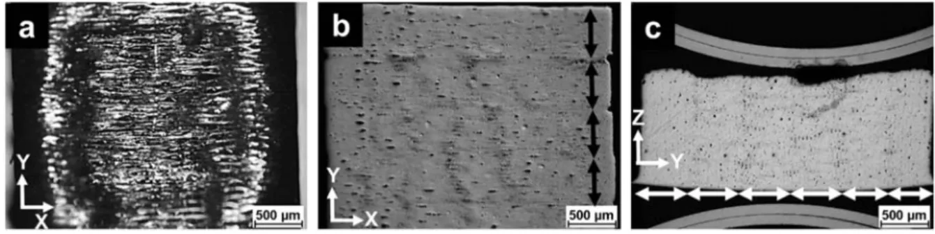
Surface morphology of the printed silver samples is shown inFig. 1. The surface of the sample (Fig. 1a) showcased an undulating pattern, commonly noted in most inkjet printed parts[10].Fig. 1b and c depict
Table 1
Process parameters used for printing and sintering AgNPs in JETx® 3D inkjet printing machine.
JETx® printing conditions JETx® sintering conditions using infrared (IR) lamp
Print resolution Printing speed Jetting voltage Print height Print head temperature IR intensity No. of passes under IR Sample height from IR source Sintering speed
600 dpi 300 mm/s 90 V 1 mm 20 °C 50% 8 5 mm 5 mm/s
the transverse section (TS) and longitudinal section (LS) of the printed samples respectively. Each arrow inFig. 1b and c indicates a segment of a print layer and each segment was measured to be approximately 500μm. This is due to the nozzle spacing of 500μm in the Spectra SE128 print head and it would need six nozzles to print the 3 mm pat-tern (i.e. 500μm × 6 = 3 mm), hence six segments. A number of black regions can be spotted within both the TS and LS of the samples. Although these spots may appear to be voids, further examination was required for confirmation.
3.2. Porosity
XCT was performed on three complete 1000 layers of 3 mm × 3 mm samples to investigate the black regions further. The reconstructed XCT data and cross sections obtained in the middle of XY, YZ and ZX planes of a sample are shown inFig. 2. In addition to the wavy surface, a trench in the middle of the printed sample can be witnessed from the XCT image of the sample (Fig. 2a). Formation of this trench could mainly be due to varied solvent evaporation at the centre and the boundary of the printed structure when the layer is exposed to the IR source, sim-ilar to a coffee-ring effect[25]. Inkjet printed patterns have previously been shown to depict such a coffee-ring effect[26,27]. Since several layers were built successively, the coffee ring effect observed for each layer added up to form such a trench.
Similar to the optical microscope images, the XCT cross sections also showed black regions. In fact, the quantity of black regions observed on the XCT data was more than that observed on the optical microscopic image inFig. 2c. This could be because during polishing, there is a chance for the eroded material (i.e. silver and the polymer from the mount) to get into the voids, whereas in XCT, a more realistic represen-tation of voids was obtained. By comparingFig. 2b and d, it can be seen that the black spots in the printed patterns are aligned almost in a straight line in both the X and Z direction. However, a similar trend was not observed in the XZ plane (Fig. 2c) and this is possibly due to the fact that the sectioning was performed in the middle of a printed sil-ver track. The distance between the two black regions i.e. the width of a silver track was measured to be ~ 86μm ± 5.3μm. This track width cor-related with the AgNP ink droplet diameter. The droplet diameter for the AgNP ink on a silver surface at room temperature was observed to be around 150μm; however, the observed track width is around half of this value. This significant difference shows that the spreading of the ink was restricted due to pinning[28].
Spreading of the ink is controlled by surface wettability which is in-fluenced by several factors and surface temperature is among them. In this study, since multiple layers are printed and exposed to IR, the sur-face was observed to remain at ~165 °C ± 5 °C. When a droplet reaches the surface, due to this surface temperature, evaporation of the solvent (TGME, boiling point = 122 °C) in the ink will commence. As a result, theflow of the ink will be restricted leading to effective pinning of the
droplet when compared to room temperature. In addition to the surface temperature, surface defects can also affect the wetting behaviour.
It should be noted that from the XCT and microscope images, the sintered tracks along the X direction showed continuity compared to those in the Y direction. One possible reason for this occurrence is due to better merging of droplets in the X direction compared to the Y direc-tion. As discussed earlier, the pattern is divided into six segments since the distance between the nozzles was 500μm. Hence, during printing, the employed six nozzles will print one complete track per segment in the X axis before moving a step (42μm) to print the next track. Since the resolution of the pattern was 600 dpi, 71 droplets are required to print a 3 mm track and the approximate time required to print a droplet was estimated to be 141.1μs. This time interval between droplet depo-sitions in the X axis was observed to be sufficient for the droplets to merge and form a continuous track. Thus the effect of surface tempera-ture on the ink wettability was less significant when printing in the X axis. Whereas for the Y axis, the time it would take to print thefirst droplet of the second track will be at least 0.13 s. This includes the time required to print the droplets in the previous track and the move-ment of the substrate to the print position. However, this does not in-clude the acceleration and deceleration time of the motors in the X and Y movement stages that needs to be accounted. During this reten-tion time, the droplets printed in the previous track are likely to be par-tially dried due to the evaporation of the solvent caused by the surface temperature. This will affect the ink wettability which will in turn affect
Fig. 1.Optical microscopic images of the 1000 layers of IJ printed and sintered AgNPs. (a) Top view (XY); (b) transverse section (XY) and (c) longitudinal (YZ) section of the sample. The arrows indicate the segments in the sample.
the merging of the droplets in the Y direction. In addition, coffee-ring ef-fects during solvent drying can also play a crucial role in the merging of droplets due to the formation of uneven morphologies in the middle and the boundaries of the deposit.
The resolution of the pattern can also be another contributing factor for this discontinuous pattern in the Y direction. The resolution (600 dpi) used in this study gives a drop spacing of 42.3μm. Since every individual track has a width of approximately 86μm, this drop spacing may not be sufficient for consistent overlapping of the droplets. As a result, the merging of droplets was restricted in the Y direction. Al-though the resolution could have contributed towards the droplet merging to a certain extent, in view of the droplets in X axis being con-tinuous, the time taken to print the next droplet in the Y direction and the surface temperature are expected to be crucial factors. The volume of the printed part obtained using the XCT was 2.9% lower than expect-ed. This deviation is possibly due to the surface irregularities/defects and varied spreading behaviour of the ink in the centre and the bound-aries due to coffee-ring effect.
3.3. Microstructure
In order to observe the coalescence of the AgNPs after exposing to IR in detail, a FEG SEM was employed to characterise the sample.Fig. 3 shows the microstructure of the printed sample obtained from the LS of the printed sample. The arrows inFig. 3a indicate the micrometre sized pores and some that have beenfilled by the eroded materials dur-ing mechanical polishdur-ing. Pores of up to 15μm size were observed on the printed samples. Since these pores are caused by insufficient merg-ing of the droplets in the Y direction, they were observed to be deep (Fig. 3b).
A network of sintered AgNPs with some nano-sized pores can be seen inFig. 3C. Due to the mechanical polishing of the samples, several streaks can be observed on the samples. The microstructure of the sintered AgNPs was observed to be almost identical in different areas of the LS of the sample (see supporting information). However, the mi-crostructure of the sintered AgNPs on the top few layers can be different since, it spends relatively less time under the IR compared to the layers beneath[22]. Grain size of the sintered AgNPs was not computed from
the obtained SEM images since an irregular morphology of the grains were observed; however, the void percentage was computed and discussed (seeDiscussionsection).
3.4. Elemental analysis
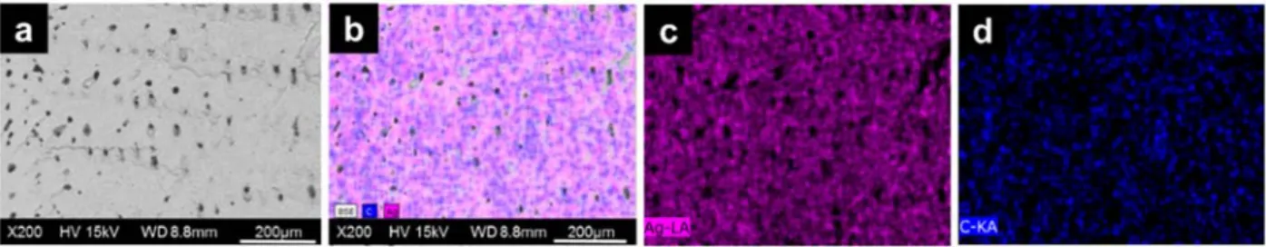
Elemental composition of the printed samples was measured using an EDX spectrometer in several arbitrary areas. The obtained atomic concentration of the detected elements (at. %) revealed that the sample is primarily composed of silver (87.7% ± 3%) with traces of oxygen (7.3% ± 4%) and carbon (5% ± 1%). Furthermore, the elemental map-ping also showed silver to be dominant on the surface (Fig. 4). It can be noted from the elemental mapping that no signal was obtained from the black regions of the sample. An analysis performed explicitly on the void showed no signal for carbon in these voids and this further confirms that these voids are not due to the ink residues (supporting in-formation). However, the existence of 5% carbon in the sample is possi-bly due to contamination from the atmosphere, silicon carbide grits, polymer resin from the mount and partially from the AgNP ink residues [29].
Carbon concentration in the atmosphere can vary significantly de-pending on the environment. However, a previous study showcased that when a thinfilm of silver was exposed to atmosphere, a significant reduction in the intensity of silver (from 99% to 66%) was noticed to-gether with a 10% increase in oxygen and 24% increase in carbon[30]. Although the carbon was mainly due to the adsorption of hydrocarbon from the atmosphere, oxygen can be due to a combination of the native oxide layer, chemisorption of oxygen species and oxygen containing carbon species[30].
3.5. Vickers hardness
Vickers hardness was obtained for the printed samples on the YZ planes at different locations. The obtained hardness (HV) value was 51 ± 1 HV. As shown previously, the existence of voids on both micro- and nanoscales is potentially the primary reason for this low value[31]. However, this can be improved by optimising the process conditions to reduce the voids in the sample.
Fig. 3.Microstructure of the printed silver sample. (a) Micrograph representing voids and the voidsfilled with eroded polymer from the mount and silver from the sample; (b) a void; (c) coalesced AgNPs and the nano-pores. The arrows indicate pores observed in the sample.
4. Discussion
Inkjet printing is attractive for a number of reasons[18]and holds the potential to satisfy the key requirements to process precious metals, including its high material utilisation rate, ease of processing and less wastage[32]. Also, high print resolution, and the ability to print multiple materials, and on planar surfaces can be attained through this non-contact printing technique compared to other lithographic methods, though other non-contact printing methods such as aerosol jet have been shown desirable for non-contact printing on freefrom surfaces [18]. Among these advantages, IJ printing is criticized for being slow in terms of producing high volume parts. However, scaling-up of inkjet printing is relatively simple, by using extra print heads, therefore, in-creasing production speed.
There is no previous detailed study on inkjet printing of multiple layers of silver to fabricate micro- or macro-scale parts from nanoparti-cles. This was mainly due to the limitations associated with existing printing equipment and ability to achieve high densities in-process. Currently available systems on the market can print a few layers of MNPs and are not usually equipped with a sintering source. The other
restriction lies in the print volume, especially in the Z direction. Since the JETx® printer used in this study was designed to overcome these prevailing issues, it was possible to print 1000 layers of AgNPs.
The size of the AgNPs play a crucial role in determining the sintering temperature since sintering of the nanoparticles is facilitated by its high surface-to-volume ratio. The size of the AgNPs used in this study is b100 nm and as a result, sintering is possible at temperatures as low as 130 °C. Sintering of AgNPs at a low temperature will be significantly useful when printing AgNPs on heat-sensitive materials. Furthermore, we demonstrated previously that the void percentage increased bottom-up as the bottom layers received more IR exposures than the successive layers. The present study showcasedb7% voids (nanoscale) whereas the previous study showed ~25%. The reduction in voids is ex-pected to be mainly due to the increase in the printing resolution from 500 dpi to 600 dpi[22]. This increase in the resolution improved the droplet merging and increased the amount of AgNPs per unit area. Fur-thermore, since 1000 layers were built in this study, prolonged expo-sure of the printed layers to the temperature (165 °C ± 5 °C) further promoted the sintering thereby reducing the voids and increased the grain size of the printed structure. Thus the size and the amount of the nanoparticles used to print was observed to contribute to the intrinsic properties of the printed part.
The sintering temperature used in this study is significantly above the boiling point of the major solvent in the silver ink, TGME. This tem-perature was chosen based on the previous literature[33]on the sintering of AgNP ink and the thermogravimetric analysis (TGA) per-formed in this study on the AgNP ink used to print the structures. The TGA showed a maximum weight loss at 186.6 °C, significantly above the boiling point of the major solvent TGME (supporting information). This increase in the transition temperature of TGME from its boiling point is likely due to the presence of other additives such as surfactants
Fig. 5.X-ray computed tomographic and SEM micrographs of 1000 layers of silver printed with 750 dpi resolution. (a) XCT scan of the complete sample; (b) transverse section of the sample in XY plane; (c) cross section of the sample in XZ plane; (d) Vertical section of the sample in YZ plane (arrows indicate cracks).
Fig. 6.Microstructure of the printed silver sample with 750 dpi. (a) Micrograph representing voids (black areas); (b) magnified image showing the sintered particle; (c) sintered AgNPs and the nano-pores. The arrows indicate scratches observed in the sample due to polishing.
that are added to the ink to maintain the stability of the dispersed AgNPs. However, a parametric study was performed to study the void percentage of samples sintered at 125 °C ± 4 °C, which is close to the boiling point of the solvent TGME. Samples sintered at this relatively low temperature for the same resolution (600dpi) had a nano-void per-cent of 7.1 which is 8.5% more than the sample sintered at 165 °C ± 5 °C (supporting information). Thus 165 °C was used to sinter the silver nanoparticles to attain a better coalesced structure with less voids.
Despite showcasing the ability of IJ printing systems to fabricate 3D parts using AgNPs, this study raised a number of questions to be ad-dressed in the future including: (1) accumulation of the coffee-ring ef-fect leading to a undesired geometry; (2) build-up of surface deef-fects altering theflow behaviour of the ink; (3) the effect of surface temper-ature on the wettability of the ink; (4) the impact of time and resolution on the merging of droplets and (5) the pores evolving as a result of these issues. In order to fabricate structures with relatively less pores and bet-ter mechanical properties, these concerns should be investigated fur-ther. Furthermore, similar to other existing metal AM processes, printed samples were also observed to warp slightly, possibly due to the build-up of thermal stresses and shrinkage due to prolonged expo-sure to the IR.
The above challenges can be addressed by using optimal process pa-rameters. For example, in order to improve the density of the sample without significant defects, the drop spacing can be modified by in-creasing the resolution of the pattern. To demonstrate this, a sample with a print resolution of 750 dpi was printed and characterised. Owing to the reduction of drop spacing from 42.3μm to 33.9μm, a sig-nificant improvement was observed with regards to the merging of droplets in the Y direction (Fig. 5). XCT scan for 1000 layers of a 750 dpi sample printed using AgNPs is shown inFig. 5. Due to an inter-nal error in the printhead rotation during printing, a misalignment was observed between the segments (Fig. 5b). As a result of misalignment during print head rotation, cracks were observed towards the internal boundaries of the segments (Fig. 5b and d). However, cross-sections of the sample inFig. 5b–d depict an improvement in the merging of the droplets compared to 600 dpi sample.
The volume of the design and the printed part for both printing res-olution was compared to study the deviation of the printed sample from actual design. The actual volume of both the 600 dpi and the 750 dpi samples obtained using XCT were 2.9% and 4.9% lower than the expect-ed volume. The surface defects and undulating surface morphology are likely to be some of the contributing factors towards this decrease. For the 750 dpi, the other contributing factor for reduced volume is the sur-face defect caused due to the blocked nozzle and the misaligned print head rotation, thus deviating more from the expected volume. The layer thickness of the 750 dpi (1.4 ± 0.1μm) sample increased by 15%
compared to 600 dpi (1.2 ± 0.1μm) due to the increase in the amount of material deposited per unit area.
On comparing the microstructure of the sample with 600 dpi and 750 dpi, the sintered particles can be observed to be more densely ar-ranged for the 750 dpi sample than 600 dpi sample (Fig. 6). This is likely due to a combination of factors including the availability of more mate-rial and better merging of droplets. In terms of the elemental composi-tion, it did not vary significantly from the 600 dpi sample since the same ink was used to build the samples with 750 dpi. However, the void per-centage (micro and nano voids) varied significantly between the 600 and 750 dpi samples.
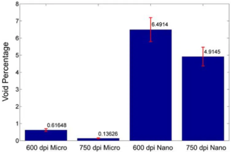
Fig. 7shows the void percentages computed using MATLAB for both print resolution and it can be witnessed that 750 dpi sample had a micro void percentage of 75% lower than the 600 dpi sample. Similarly, 24% lower nano void percentage was accounted for the 750 dpi sample than the 600 dpi sample. As mentioned before, the micro voids in the 600 dpi sample are primarily caused by the insufficient merging of the printed tracks in Y direction. When the print resolution was increased to 750 dpi, better merging of printed lines significantly reduced these voids. Due to the presence of more material per unit area compared to the 600 dpi, the sintering of AgNPs in 750 dpi was enhanced, leading to this 25% decrease in nano voids.
Currently using the EOS Precious M 080, fully dense parts can be fab-ricated; but printing multi-material parts is still a challenge. Attaining 100% dense structures by inkjet printing of nanoparticles will be chal-lenging; however, post-processing of the printed structure may possibly improve the density. The Vickers hardness of the printed samples were 51 HV for 600 dpi and 66 HV for 750 dpi. This observed 29% increase in hardness between the print resolutions is likely due to the reduced micro and nano voids in the 750 dpi than the 600 dpi sample thus show-ing the impact of voids on the hardness of the printed samples.
In contrast, the hardness obtained for the printed samples of both dpi are higher than the bulk as-cast commercially pure silver (26 HV), close to sterling silver (75 HV) and cold-worked silver[34]. However, cold-worked silver was observed to showcase Vickers hardness typical-ly above 75 HV depending on the processing conditions[35]. The exis-tence of carbon, oxygen and possibly fraction of other metals in the sample matrix and exposure of the printed layers to IR power source for prolonged time may alter the microstructure and thus increasing the hardness of the printed sample compared to the conventional as-cast samples. Similar increase in the hardness compared to the bulk was previously reported. With a porosity of 12.5%, Khan and Dickens [5]obtained Vickers hardness of 17% more than the bulk material and revealed the increase in the hardness than the bulk is likely due to the varied microstructure. Similarly, nano-indentation of SLM processed pure gold showcased an equivalent Vickers hardness of 28 HV, 20%
higher than the pure as-cast gold[6]. This reported increase in the hard-ness was attributed to the varied heating and cooling rates compared to the as-cast material. Thus, the print resolution can be one of the contrib-utors to attain parts with improved mechanical properties.
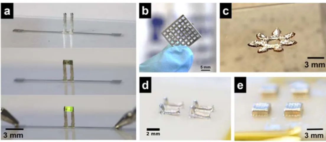
5. Demonstrators
In order to demonstrate the ability of inkjet printing to print micro and macro parts from nano particles, AgNP ink was used to print the structures shown inFig. 8. Since these samples were printed on a glass slide and due to its high wettability compared to the ceramic substrates, 500 dpi resolution was used for all the patterns. The printing and sintering conditions were same as the 600dpi samples given in the methods section.
6. Conclusion
The potential to use IJ printing of AgNPs for building macroscopic parts has been demonstrated. Print resolution, surface temperature, sur-face defects,flow behaviour and wettability of the ink on the surface were observed to affect the merging of droplets, leading to voids in the sample. Further optimisation in print resolution from 600 dpi to 750 dpi was observed to improve the merging of droplets and reduced the micro voids to 75% and nano voids to 24%. This reduction in voids contributed to the improved Vickers hardness, 29% more than the 600 dpi sample. Thus, by selecting optimal print resolution, dense parts can be printed and precious metals can be processed through inkjet printing.
Acknowledgement
This work was supported by the Engineering and Physical Sciences Research Council [grant numbers EP/I033335/2, EP/L01534X/1, EP/ M008983/1], the authors acknowledge the assistance of Mr. Martin Roe with SEM at the Nanoscale and Microscale Research Centre (NMRC) at The University of Nottingham.
Appendix A. Supplementary data
Image processing in MATLAB for micro voids (S1) and nano voids (S2); SEM cross section showing the microstructure of the sample in dif-ferent regions of the sample (S3); EDX elemental mapping performed on a void region (S4); Thermogravimetric analysis of AgNPs ink (S5); Image analysis of 600 dpi samples printed at 125 ± 4 °C (S6). Supple-mentary data associated with this article can be found in the online ver-sion, athttps://doi.org/10.1016/j.matdes.2017.10.070.
References
[1] I. Gibson, D.W. Rosen, B. Stucker, Additive Manufacturing Technologies, Springer US, 2010.
[2] D. Zito, A. Carlotto, A. Loggi, P. Sbornicchia, D. Bruttomesso, S.A. Progold, Definition and solidity idity of gold and platinum jewels produced using Selective Laser Melt-ing SLM™technology, Santa Fe Symposium on Jewelry Manufacturing Technology 2015, pp. 439–470.
[3] F. Cooper, Do the new, low-cost photopolymer 3D printers now becoming available have a place in the jewelry manufacturing environment? Santa Fe Symposium on Jewelry Manufacturing Technology 2016, pp. 143–164.
[4] K. Abernathy, Future trends in digital design and additive manufacturing, Santa Fe Symposium on Jewelry Manufacturing Technology 2016, pp. 1–22.
[5] M. Khan, P. Dickens, Selective laser melting (SLM) of gold (Au), Rapid Prototyp. J. 18 (1) (2012) 81–94.
[6] M. Khan, P. Dickens, Selective laser melting (SLM) of pure gold for manufacturing dental crowns, Rapid Prototyp. J. 20 (6) (2014) 471–479.
[7] D. Zito, A. Carlotto, A. Loggi, P. Sbornicchia, D. Maggian, S.A. Progold, et al., Optimiza-tion of SLM technology main parameters in the producOptimiza-tion of gold and platinum jewelry, Santa Fe Symposium on Jewelry Manufacturing Technology 2014, pp. 439–470.
[8] U.E. Klotz, D. Tiberto, F. Held, Additive manufacturing of 18-karat yellow-gold alloys, Santa Fe Symposium on Jewelry Manufacturing Technology 2016, pp. 255–272. [9] E. MacDonald, R. Wicker, Multiprocess 3D printing for increasing component
func-tionality, Science 353 (6307) (2016) aaf2093-1–aaf2093-8.
[10] F. Zhang, C. Tuck, R. Hague, Y. He, E. Saleh, Y. Li, et al., Inkjet printing of polyimide insulators for the 3D printing of dielectric materials for microelectronic applications, J. Appl. Polym. Sci. 133 (18) (2016).
[11] S. Jang, Y. Seo, J. Choi, T. Kim, J. Cho, S. Kim, et al., Sintering of inkjet printed copper nanoparticles forflexible electronics, Scr. Mater. 62 (5) (2010) 258–261. [12] H.S. Kim, J.S. Kang, J.S. Park, H.T. Hahn, H.C. Jung, J.W. Joung, Inkjet printed
electron-ics for multifunctional composite structure, Compos. Sci. Technol. 69 (7–8) (2009) 1256–1264.
[13] R. Vyas, V. Lakafosis, H. Lee, G. Shaker, L. Yang, G. Orecchini, et al., Inkjet printed, self powered, wireless sensors for environmental, gas, and authentication-based sens-ing, IEEE Sensors J. 11 (12) (2011) 3139–3152.
[14]J. Niittynen, R. Abbel, M. Mäntysalo, J. Perelaer, U.S. Schubert, D. Lupo, Alternative sintering methods compared to conventional thermal sintering for inkjet printed silver nanoparticle ink, Thin Solid Films 556 (2014) 452–459.
[15] A. Chiolerio, M. Cotto, P. Pandolfi, P. Martino, V. Camarchia, M. Pirola, et al., Ag nanoparticle-based inkjet printed planar transmission lines for RF and microwave applications: considerations on ink composition, nanoparticle size distribution and sintering time, Microelectron. Eng. 97 (2012) 8–15.
[16] B.J. Kang, C.K. Lee, J.H. Oh, All-inkjet-printed electrical components and circuit fabri-cation on a plastic substrate, Microelectron. Eng. 97 (4023) (2012) 251–254. [17] A. Bonea, A. Brodeala, M. Vlǎdescu, P. Svasta, Electrical conductivity of inkjet printed
silver tracks, Proceedings of the International Spring Seminar on Electronics Tech-nology 2012, pp. 1–4.
[18] Z.P. Yin, Y.A. Huang, N.B. Bu, X.M. Wang, Y.L. Xiong, Inkjet printing forflexible elec-tronics: materials, processes and equipments, Chin. Sci. Bull. 55 (30) (2010) 3383–3407.
[19] A. Denneulin, A. Blayo, C. Neuman, J. Bras, Infra-red assisted sintering of inkjet printed silver tracks on paper substrates, J. Nanopart. Res. 13 (9) (2011) 3815–3823. [20] S.H. Yoon, J.H. Lee, P.C. Lee, J. Do Nam, H.-C. Jung, Y.S. Oh, et al., Sintering and consol-idation of silver nanoparticles printed on polyimide substratefilms, Macromol. Res. 17 (8) (2009) 568–574.
[21]J. Perelaer, B.J. De Gans, U.S. Schubert, Ink-jet printing and microwave sintering of conductive silver tracks, Adv. Mater. 18 (16) (2006) 2101–2104.
[22]J. Vaithilingam, M. Simonelli, E. Saleh, N. Senin, R.D. Wildman, R.J.M. Hague, et al., Combined inkjet printing and infra-red sintering of silver nanoparticles using a swathe-by-swathe and layer-by-layer approach for 3-dimensional structures, ACS Appl. Mater. Interfaces 9 (2017) 6560–−6570.
[23] XJET [Internet], [cited 2017 Jan 15]. Available from:http://www.xjet3d.com/. [24] A. Thompson, I. Maskery, R.K. Leach, X-ray computed tomography for additive
manufacturing: a review, Meas. Sci. Technol. 27 (7) (2016) 72001.
[25] R.D. Deegan, O. Bakajin, T.F. Dupont, G. Huber, S.R. Nagel, T.A. Witten, Capillaryflow as the cause of ring stains from dried liquid drops, Lett. Nat. 389 (1997) 827–829. [26] D. Soltman, V. Subramanian, Inkjet-printed line morphologies and temperature
con-trol of the coffee ring effect, Langmuir 24 (5) (2008) 2224–2231.
[27] D. Tobjörk, H. Aarnio, P. Pulkkinen, R. Bollström, A. Määttänen, P. Ihalainen, et al., IR-sintering of ink-jet printed metal-nanoparticles on paper, Thin Solid Films 520 (7) (2012) 2949–2955.
[28] S. Vafaei, C. Tuck, R. Wildman, I. Ashcroft, Spreading of the nanofluid triple line in ink jet printed electronics tracks, Addit. Manuf. 11 (2016) 77–84.
[29]J. Vaithilingam, E. Prina, R.D. Goodridge, R.J.M. Hague, S. Edmondson, F.R.A.J. Rose, et al., Surface chemistry of Ti6Al4V components fabricated using selective laser melting for biomedical applications, Mater. Sci. Eng. C. 67 (2016) 294–303. [30] A. Matikainen, T. Nuutinen, T. Itkonen, S. Heinilehto, J. Puustinen, J. Hiltunen, et al.,
Atmospheric oxidation and carbon contamination of silver and its effect on surface-enhanced Raman spectroscopy (SERS), Sci Rep 6 (1) (2016) 1–5. [31]M. Khan, P. Dickens, Selective Laser Melting (SLM) of pure gold, Gold Bull. 43 (2)
(2010) 114–121.
[32] A. Kamyshny, J. Steinke, S. Magdassi, Metal-based inkjet inks for printed electronics, Open Appl. Phys. J. 4 (1) (2011) 19–36.
[33] W. Zhou, F.A. List, C.E. Duty, S.S. Babu, Sintering kinetics of inkjet-printed conductive silver lines on insulating plastic substrate, Metall. Mater. Trans. B 46 (3) (2015) 1542–1547.
[34] Butler JR. An improved sterling silver alloy and articles made from the same [Inter-net]. United STates Patent and Trademark Office; 2013. Available from:http://www. google.co.uk/patents/WO2013032665A1?cl=en