Experimental Implementation of a Linear Control
Technique for a Single-Phase Matrix Converter
M. Rivera, S. Rojas
Universidad de Talca
Department of Ind. Tech., Curico, CHILE Email: [email protected]
http://www.utalca.cl
P. Wheeler
University of Nottingham Nottingham, U.K.
Email: [email protected] http://www.nottingham.ac.uk
V. Yaramasu
Northern Arizona University
Department of EECS, Flagstaff, AZ, USA Email: [email protected]
http://www.nau.edu
Abstract—This paper describes a matrix converter with a three-phase input and single-phase output that can be used as a building block for high-power cascaded converters. In this paper a sinusoidal pulse width modulation technique with a linear controller is proposed for the single-phase output matrix con-verter. The proposed modulation and control will be used in the cascade configurations for high-power applications. Simulation and experimental results are presented to validate the proposed modulation and control approach.
NOMENCLATURE Variable Description
vi Input voltage [v
AvBvC]
T
ii Input current [i
AiBiC]
T
v Load voltage v+
−v−
io Load current
Cf Input filter capacitor
I. INTRODUCTION
The matrix converter (MC) consists of an array of bidirec-tional switches, which are used to directly connect the power supply to the load without using any dc-link or large energy storage elements [1].
The most important characteristics of matrix converters are: 1) a simple and compact power circuit; 2) generation of load voltage with arbitrary amplitude and frequency; 3) sinusoidal input and output currents; 4) operation with unity power factor; 5) regeneration capability. These highly attractive characteris-tics are the reason for the tremendous interest in this topology [2], [3]. The major drawbacks for matrix converters include: 1) absence of ride-through capability, and 2) perturbations in the input side are reflected on the output side due to the absence of storage elements.
Research on matrix converters began with the work of Venturini and Alesina in 1980 [2]. They provided the rigorous mathematical background and introduced the name “matrix converter”, elegantly describing how the low-frequency be-havior of the voltages and currents which are generated at the converters input and output. One of the biggest difficulties in the operation of this converter was the commutation of current between the bidirectional switches [4]. This problem has been solved by introducing intelligent and soft commutation techniques, giving new momentum to research in the area.
The development of this converter is now reaching industrial applications [1]. At least one major manufacturer of power converters (Yaskawa) is now offering a complete line of standard units for up to several megawatts and medium voltage using a cascade connection of converters. These units have rated power (and voltages) of 9-114 kVA (200 V and 400 V) for a low voltage MC, and 200-6,000 kVA (3.3 kV, 6.6 kV) for medium voltage operation [1].
Years of continuous effort have been dedicated to the development of different modulation and control strategies that can be applied to matrix converters [4]–[11]. Pulse width modulation (PWM) is a classic modulation technique used to digitally control the commutation of switches in a power converter. Originally this technique was employed in inverters, but due its robustness and simplicity this have been for different power converter topologies, being a very well know and used technique at the industrial level. To realized closed-loop control, a modulation stage is used in conjunction with the linear PI regulators.
In this paper, experimental implementation of a sinusoidal pulse width modulation (SPWM) with a linear controller is proposed for a single-phase matrix converter. This converter is the basic cell of the converter presented in [1]. Simula-tion and experimental results are presented to validate the implementation. As well the proposed modulation has been presented in [12], here we demonstrate the performance of this by experiments.
II. TOPOLOGY ANDMATHEMATICALMODEL OF THE
SINGLE-PHASEMATRIXCONVERTER
The mathematical model of the single-phase matrix con-verter is obtained from Fig. 1 where is shown the multi-modular power topology. The output voltagev= [vp−vn]is a
function of the converter’s switch states and the input voltages vi:
vp=
S1 S2 S3
vi, (1)
vn=
S4 S5 S6
v
i. (2)
vA
vB
vC
iA
iB
iC
io vp
vn Cf
S1
S2
S3
S4
S5
[image:2.612.179.534.49.479.2]S6
Fig. 1. Topology of the single-phase matrix converter.
converter’s switch states and the load current io:
ii=
S1−S4
S2−S5
S3−S6
io. (3)
These equations correspond to the nine valid switching states of the converter [12] and the restrictions of no short circuits in the input and no open lines in the output.
Finally, assuming an inductive-resistive load, the following equation describes the behavior of the load:
dio
dt =
1
Lv− R
Lio. (4)
III. SINUSOIDALPULSEWIDTHMODULATION FOR THE
SINGLE-PHASEMATRIXCONVERTER
Sinusoidal pulse width modulation (SPWM) generates the switching pulses which are proportional to the amplitude of a reference signal (vref), which consists in a sinusoidal signal
that is compared to a triangular carrier signal (vtri). The
structure of this kind of modulation is shown in Fig. 2, where is also possible to observe two blocks coupled to the output (N) which generates two other signals based the value ofNshown in Fig. 3. In a three-phase system it is necessary to identify the different sectors of the input voltage as indicated in Fig. 4. The different sectors are given byxA,xB andxC, which are
generated using binary comparators. With this information it is possible to obtain the switching signals as shown in Table I. The control scheme is composed of the modulation block and a PI controller (Fig. 5). Generally a PI controller is used but in this case the PI was considered for the better observed results.
IV. SIMULATION ANDEXPERIMENTALRESULTS
Simulation and experimental results are presented in order to validate the proposal. The simulation has been implemented
-1
+
00
N N1
vref
vtri
[image:2.612.71.280.52.276.2]N2
Fig. 2. Unipolar modulation scheme.
vtri
−vref +vref
+vref > vtri
−vref > vtri
N
a)
b)
c)
Fig. 3. Signals generated for the unipolar SWPM technique.
1 1 1
1 1 1
1 1 1
1 4
3
2 5
6
0 0 0
0 0 0 0 0 0
va
vb
vc
va vb vc
xa
xb
xc xa xb xc
Sector
a) b)
Fig. 4. Sectors obtained from the input voltages.
using Gecko Circuits Software from ETH Zurich and the ex-perimental validation has been done in the Energy Conversion and Power Electronics Research Laboratory (LCEEP) at the University of Talca. The parameters used in both simulation and experimental evaluation are detailed in Table II.
[image:2.612.322.527.60.326.2]TABLE I
GENERATION OF SWITCHING PULSES
X/Y Binary Signals Sector Output Switching pulses
N1 N0 xA xB xC X vo vo S1 S2 S3 S4 S5 S6
1 0 1 1 1 0 6 viA viC 1 0 0 0 0 1
2 0 1 0 1 0 2 viB viC 0 1 0 0 0 1
3 0 1 0 1 1 3 viB viA 0 1 0 1 0 0
4 0 1 0 0 1 1 viC viA 0 0 1 1 0 0
5 0 1 1 0 1 5 viC viB 0 0 1 0 1 0
6 0 1 1 0 0 4 viA viB 1 0 0 0 1 0
7 1 1 1 1 0 6 viC viA 0 0 1 1 0 0
8 1 1 0 1 0 2 viC viB 0 0 1 0 1 0
9 1 1 0 1 1 3 viA viB 1 0 0 0 1 0
10 1 1 0 0 1 1 viA viC 1 0 0 0 0 1
11 1 1 1 0 1 5 viB viC 0 1 0 0 0 1
12 1 1 1 0 0 4 viB viA 0 1 0 1 0 0
13 0 0 1 1 0 6 viC viC 0 0 1 0 0 1
14 0 0 0 1 0 2 viC viC 0 0 1 0 0 1
15 0 0 0 1 1 3 viA viA 1 0 0 1 0 0
16 0 0 0 0 1 1 viA viA 1 0 0 1 0 0
17 0 0 1 0 1 5 viB viB 0 1 0 0 1 0
18 0 0 1 0 0 4 viB viB 0 1 0 0 1 0
TABLE II
PARAMETERS USED IN BOTH SIMULATION AND EXPERIMENTAL VALIDATION
Variables Description Value vi Source voltage 50, 100 [Vpk]
fi Source frequency 50 [Hz]
fs Sampling frequency 10, 20, 40 [kHz]
R Load resistance 10 [Ω]
L Load inductance 10 [mH]
io Reference amplitude 3, 6 [Apk] fo Reference frequency 25, 50 [Hz]
+
_ Unipolar
SPWM
Circuit Logic
Converter Source
PI
LL
RL
iref
imes vtri
vi
N
Ssws
Fig. 5. Scheme of the PI+SPWM control strategy
V. DISCUSSION
During the implementation and validation of the control strategy different issues were observed. At higher sampling frequency, the tracking of the current to its reference is better. This is an obvious comment, however it is important to highlight that the selection of the sampling time implies in the tracking.
By increasing the sampling frequency, the switching pulses
are updated faster at the cost of more calculations in a short time period. The performance of the strategy is much better when the source frequency is higher than the output reference frequency, because the tracking of the load current to its reference is better due to the fact that there are more available vectors to be applied in the converter. The modulation method in [12] is used in this work to obtain experimental results under different operating conditions.
In order to mathematically verify the tracking of the load current to its reference, the percentage absolute average error given by eq. (5) is evaluated.
eexp=
Pn
i=1||io|−|iref||
n
×100
Airef
(5)
where,
io Load current [A]
iref Load current reference [A]
n Number of processed data
Airef Amplitude of load current reference [A]
0 0.01 0.02 0.03 0.04 0.05 0.06 −10
−5 0 5 10
0 0.01 0.02 0.03 0.04 0.05 0.06
−200 −100 0 100 200 a)
b)
[image:4.612.326.543.65.237.2]Time [s]
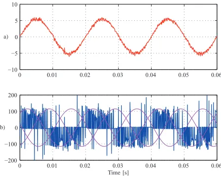
Fig. 6. Simulation results in steady state:io=6 Apk; fo=50 Hz;fs = 20
kHz;vi = 56 Vpk.
0 0.01 0.02 0.03 0.04 0.05 0.06
−10 −5 0 5 10
0 0.01 0.02 0.03 0.04 0.05 0.06
−200 −100 0 100 200 a)
b)
Time [s]
Fig. 7. Simulation results in steady state:io=6 Apk; fo=50 Hz;fs = 40
kHz;vi = 56 Vpk.
The Total Harmonic Distortion (THD) is also evaluated for both simulation and experimental results. The analysis is done for the load current as shown in Table IV. A higher sampling frequencies the THD values decrease, as expected.
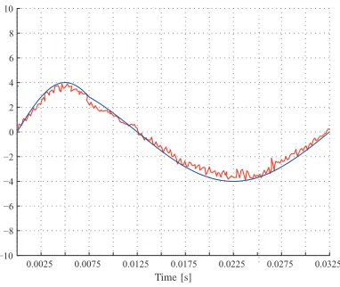
Fig. 14 and Fig. 15 show simulation and experimental results for a step amplitude change from 3[Apk] to 6 Apk. The current takes 1,38 ms in to reach steady state in simulation and 1,54 ms in the experimental validation. In Fig. 16 and Fig. 17 simulation and experimental results are shown for a
TABLE III
ABSOLUTE AVERAGE ERROR OFiRefVERSUSioATfo = 50Hz
Sampling (fs) Amplitude (io) Error (esim) Error (eexp)
10[kHz] 6[Apk] 6,926% 13,302%
20[kHz] 6[Apk] 3,744% 9,342%
40[kHz] 6[Apk] 2,341% 7,0524%
0 0.01 0.02 0.03 0.04 0.05 0.06
−10 −5 0 5 10
0 0.01 0.02 0.03 0.04 0.05 0.06
−200 −100 0 100 200 a)
b)
[image:4.612.63.284.65.237.2]Time [s]
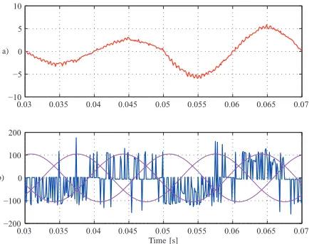
Fig. 8. Experimental results in steady state:io=6 Apk;fo=50 Hz;fs = 20
kHz;vi = 56 Vpk.
0 0.01 0.02 0.03 0.04 0.05 0.06
−10 −5 0 5 10
0 0.01 0.02 0.03 0.04 0.05 0.06
−200 −100 0 100 200 a)
b)
Time [s]
Fig. 9. Experimental results in steady state:io=6 Apk;fo=50 Hz;fs = 40
kHz;vi = 56 Vpk.
step frequency change from 50[Hz] to 25[Hz]. In all these cases is observed a very good performance of the implemented controller.
VI. CONCLUSION
The implementation of a linear current controller for a single-phase matrix converter has been presented and dis-cussed in this paper.
TABLE IV
THDOF THE LOAD CURRENT ATfo = 50Hz
Sampling (fs) Amplitude (io) THD Sim. (io) THD Exp. (io)
10[kHz] 6[Apk] 10,957% 11,763%
20[kHz] 6[Apk] 5,171% 10,680%
[image:4.612.325.543.295.468.2] [image:4.612.63.281.295.468.2]0.01 0.015 0.02 0.025 0.03 0.035 0.04 0.045 0.05 −10
−5 0 5 10
0.01 0.015 0.02 0.025 0.03 0.035 0.04 0.045 0.05
−200 −100 0 100 200 a)
b)
[image:5.612.63.283.64.238.2]Time [s]
Fig. 10. Simulation results in transient state:io=3-6 Apk;fo=50 Hz;fs=
10 kHz;vi = 56 Vpk.
0.03 0.035 0.04 0.045 0.05 0.055 0.06 0.065 0.07
−10 −5 0 5 10
0.03 0.035 0.04 0.045 0.05 0.055 0.06 0.065 0.07
−200 −100 0 100 200 a)
b)
Time [s]
Fig. 11. Experimental results in transient state:io=3-6 Apk;fo=50 Hz;fs
= 10 kHz;vi = 56 Vpk.
The simulation and experimental results demonstrated that the presented strategy provides good tracking of the output current to its reference in both steady-state and transient operating conditions.
ACKNOWLEDGMENTS
This publication was made possible by the Newton Picarte Project EPSRC: EP/N004043/1: New Configurations of Power Converters for Grid Interconnection Systems / CONICYT DPI20140007.
REFERENCES
[1] E. Yamamoto, H. Hara, T. Uchino, M. Kawaji, T. Kume, J. K. Kang, and H.-P. Krug, “Development of mcs and its applications in industry [industry forum],” Industrial Electronics Magazine, IEEE, vol. 5, no. 1, pp. 4 –12, march 2011.
[2] M. Venturini, “A new sine wave in sine wave out, conversion technique which eliminates reactive elements,” Powercon 7, 1980, pp. E3/1–E3/15, Mar. 2001.
0.03 0.04 0.05 0.06 0.07 0.08 0.09
−10 −5 0 5 10
0.03 0.04 0.05 0.06 0.07 0.08 0.09
−200 −100 0 100 200 a)
b)
[image:5.612.325.544.65.238.2]Time [s]
Fig. 12. Simulation results in transient state:io=4 Apk;fo=50-25 Hz;fs
= 20 kHz;vi= 56 Vpk.
0.03 0.04 0.05 0.06 0.07 0.08 0.09
−10 −5 0 5 10
0.03 0.04 0.05 0.06 0.07 0.08 0.09
−200 −100 0 100 200 a)
b)
Time [s]
Fig. 13. Experimental results in transient state:io=4 Apk; fo=50-25 Hz;
fs = 20 kHz;vi = 56 Vpk.
[3] J. Rodriguez, E. Silva, F. Blaabjerg, P. Wheeler, J. Clare, and J. Pontt, “Matrix converter controlled with the direct transfer function approach: analysis, modelling and simulation,” Taylor and Francis-International
Journal of Electronics, vol. 92, no. 2, pp. 63 –85, Feb. 2005.
[4] L. Zhang, C. Watthanasarn, and W. Shepherd, “Control of ac-ac matrix converters for unbalanced and/or distorted supply voltage,” Power
Elec-tronics Specialists Conference, 2001. PESC. 2001 IEEE 32nd Annual,
vol. 2, pp. 1108 –1113 vol.2, 2001.
[5] G. Roy and G.-E. April, “Cycloconverter operation under a new scalar control algorithm,” Power Electronics Specialists Conference, 1989.
PESC ’89 Record., 20th Annual IEEE, pp. 368 –375 vol.1, Jun. 1989.
[6] J. Rodriguez, “High performance dc motor drive using a pwm rectifier with power transistors,” Electric Power Applications, IEE Proceedings
B, vol. 134, no. 1, p. 9, Jan. 1987.
[7] L. Huber and D. Borojevic, “Space vector modulated three-phase to three-phase matrix converter with input power factor correction,”
Indus-try Applications, IEEE Transactions on, vol. 31, no. 6, pp. 1234 –1246,
Nov. 1995.
[image:5.612.64.281.293.465.2] [image:5.612.325.543.295.466.2]0 0.0025 0.005 0.0075 0.01 0.0125 0.015 0.0175 0.02 −10
−8 −6 −4 −2 0 2 4 6 8 10
[image:6.612.83.268.64.218.2]Time [s]
Fig. 14. Simulation results under an amplitude step change:io=3-6 Apk; fo=50 Hz;fs= 40 kHz;vi= 112 Vpk.
0 0.0025 0.005 0.0075 0.01 0.0125 0.015 0.0175 0.02 −10
−8 −6 −4 −2 0 2 4 6 8 10
[image:6.612.344.533.127.288.2]Time [s]
Fig. 15. Experimental results under an amplitude step change:io=3-6 Apk; fo=50 Hz;fs= 40 kHz;vi= 112 Vpk.
[9] I. Takahashi and T. Noguchi, “A new quick response and high efficency control strategy for an induction motor,” Industrial Electronics, IEEE
Transactions on, vol. 22, no. 5, pp. 820 –827, Sep. 1986.
[10] S. Muller, U. Ammann, and S. Rees, “New time-discrete modulation scheme for matrix converters,” Industrial Electronics, IEEE Transactions
on, vol. 52, no. 6, pp. 1607 – 1615, Dec. 2005.
[11] M. Rivera, R. Vargas, J. Espinoza, and J. Rodriguez, “Behavior of the predictive dtc based matrix converter under unbalanced ac-supply,”
Power Electronics Specialists Conference, 2008. PESC 2008. IEEE, pp.
202 –207, Sep. 2007.
[12] C. Rojas, J. Rodriguez, A. Iqbal, H. Abu-Rub, A. Wilson, and S. Moin Ahmed, “A simple modulation scheme for a regenerative cascaded matrix converter,” in IECON 2011 - 37th Annual Conference
on IEEE Industrial Electronics Society, nov. 2011, pp. 4361 –4366.
0.0025 0.0075 0.0125 0.0175 0.0225 0.0275 0.0325 −10
−8 −6 −4 −2 0 2 4 6 8 10
[image:6.612.82.268.273.432.2]Time [s]
Fig. 16. Simulation results under an frequency step change: io=4 Apk; fo=50-25 Hz;fs= 40 kHz;vi= 112 Vpk.
0.0025 0.0075 0.0125 0.0175 0.0225 0.0275 0.0325 −10
−8 −6 −4 −2 0 2 4 6 8 10
Time [s]
[image:6.612.344.535.467.628.2]