This paper is published in:
S.A. Krasnikov, S.I. Bozhko, K. Radican, O. Lübben, B.E. Murphy, S.-R. Vadapoo, H.-C. Wu, M. Abid, V.N. Semenov, and I.V. Shvets, Self-Assembly and Ordering of C60 on the WO2/W(110) Surface. Nano Research 4 (2011) 194-203.
Self-Assembly and Ordering of C
60on the WO
2/W(110) Surface
S. A. Krasnikov1,*, S. I. Bozhko1, 2, K. Radican1, O. Lübben1, B. E. Murphy1, S.-R. Vadapoo1, H.-C. Wu1, M. Abid1, 3, V. N. Semenov2, and I. V. Shvets1
1 Centre for Research on Adaptive Nanostructures and Nanodevices (CRANN), School of
Physics, Trinity College Dublin, Dublin 2, Ireland;
2 Institute of Solid State Physics, Russian Academy of Sciences, Chernogolovka, Russian
Federation;
3 King Abdullah Institute for Nanotechnology, College of Science King Saud University,
Riyadh 11451, Saudi Arabia.
Abstract
The growth and ordering of C60 molecules on the WO2/W(110) surface have been
studied by low-temperature scanning tunnelling microscopy and spectroscopy (STM and STS), low-energy electron diffraction (LEED) and density functional theory (DFT) calculations. The results indicate the growth of a well-ordered C60 layer on the WO2/W(110)
surface in which the molecules form a close-packed hexagonal structure with a unit cell parameter equal to 0.95 nm. The nucleation of the C60 layer starts at the substrate’s inner step
edges. Low-temperature STM of C60 molecules performed at 78 K demonstrates
well-resolved molecular orbitals within individual molecules. In the C60 monolayer on the
WO2/W(110) surface, the molecules are aligned in one direction due to intermolecular
interaction, as shown by the ordered molecular orbitals of individual C60. STS data obtained
from the C60 monolayer on the WO2/W(110) surface are in good agreement with DFT
calculations.
1. Introduction
The fabrication of complex organic molecular structures on technologically important substrates held together by weak and reversible van der Waals interactions, hydrogen bonds or electrostatic interactions has been a much investigated topic in the past ten years [1–10]. This controlled self-assembly of organic nanostructures offers a number of powerful approaches for the development of organic molecule-based devices, which possess functions such as rectifying, switching and sensing [1–8, 11–13]. Fullerenes have attracted considerable attention in recent years due to their potential in surface chemistry and nanotemplating [13], non-linear optics [13, 14], single-molecule transistors [11, 15], and especially molecular electronics because of their tunable electronic properties, resulting in superconducting or semiconducting behaviour [11, 16, 17]. The formation and characterisation of fullerene adlayers on surfaces are of great interest from the fundamental and technological points of view because they provide valuable information about molecule interactions and can lead to potential applications in existing technologies. The study of these surface-supported systems is important for future developments in molecular electronics, since they represent promising materials for applications in advanced nanopatterning, surface templating, molecular data storage, solar cells, sensors/molecular recognition and functional surfaces [11, 13–20].
Of particular interest are the nature of the bonding between the fullerene molecules and the substrate, as reflected in the electronic charge distribution and their geometric configuration at the interface, and the dynamics of electron–hole transfer between the molecule and the metal or semiconductor surface. This information can be obtained by using a combination of scanning tunnelling microscopy and spectroscopy (STM and STS). STM is a highly local technique that has become a powerful tool for studying the adsorption geometry and the conformation and dynamics of single organic molecules and molecular assemblies on conducting substrates [1–10]. Over the last decade STM has been used intensively for the study of C60 self-assembled layers on a variety of metal [21–36] and
semiconductor [18, 37–41] surfaces. On most surfaces fullerene molecules self-assemble into close-packed monolayers with a hexagonal or quasi-hexagonal structure and a molecule– molecule separation close to 1 nm, as observed in bulk C60 [18, 21–25, 27–38, 41]. In some
cases the formation of a C60 monolayer leads to an adsorbate-induced reconstruction of the
substrate [22, 28, 30–36]. Surprisingly, only few studies of C60 on metal oxide surfaces have
been performed to this end [42–44]. This is despite the fact that metal oxide surfaces and thin films have many potential applications in existing technologies [45–49] and may be used as nanostructured templates with preformed surface patterns [50–53] for molecular self-assembly.
The importance of molecule–substrate interfaces for device performance cannot be overestimated as they determine charge injection and charge flow in the molecular devices. While STM images elucidate the topographic structure of the interface, they provide little information about its electronic properties. STS is one of the best tools for probing local electronic structure with molecular spatial resolution [5, 9, 10, 25–30, 54, 55]. STS is unique in that it allows both the filled and empty state density at the surface to be probed in a single measurement, providing local density of states information close to the Fermi level. This information is vital for understanding the properties of organic molecules and their utilization in molecular electronic devices.
In the present work, by using STM/STS, LEED and DFT calculations, we focus for the first time on the molecular self-assembly of C60 on the WO2/W(110) surface in the
submonolayer to monolayer regimes in order to reveal the conformational behaviour of C60
molecules. STS and DFT are utilised to obtain information about the local density of states. The results of this work yield important information about the electronic and structural properties of C60 molecules adsorbed on the WO2/W(110) surface.
2. Experimental details
The STM/STS experiments were performed at liquid nitrogen temperature (78 K), using a commercial instrument from Createc, in an ultra-high-vacuum (UHV) system consisting of an analysis chamber (with a base pressure of 2 × 10–11 mbar) and a preparation
chamber (5 × 10–11 mbar). An electrochemically-etched monocrystalline W(100) tip was used
to record STM images in constant current mode. The voltage Vsample corresponds to the
sample bias with respect to the tip. No drift corrections have been applied to any of the STM images presented in this paper. Tunnelling spectra in a z(V) form were acquired on an individual C60 molecule. For z(V) spectroscopy, the feedback is on while the voltage ramp is
A W(110) single crystal, prepared at the Institute of Solid State Physics RAS, was used as the substrate. An atomically-clean W(110) surface was prepared by in situ annealing at 1900 K in an oxygen atmosphere of 1 × 10⁻⁷ mbar, followed by a series of high temperature
flashes at 2200 K. The sample was heated by electron beam bombardment and temperatures were measured using an optical pyrometer (Ircon UX20P, emissivity 0.35). The clean W(110) surface was verified by LEED and STM before oxidation. Once a clean surface was obtained, the sample was oxidised at 1600 K in an oxygen atmosphere of 1 × 10⁻⁶ mbar for
60 minutes. The quality of the resulting oxide structure was verified by LEED and STM before the deposition of C60 molecules.
C60 (Aldrich Chemicals) was evaporated in a preparation chamber isolated from the
STM chamber at a rate of about 0.2 ML (monolayer) per minute from a deposition cell operated at a temperature of approximately 700 K. Before evaporation, the C60 powder was
degassed for about 8 h to remove water vapour. The total pressure during C60 deposition was
in the 10–9 mbar range and the substrate was kept at room temperature. After deposition the sample was transferred into the STM and cooled down to 78 K for measurements.
[image:3.595.104.247.318.606.2]3. Results and discussion
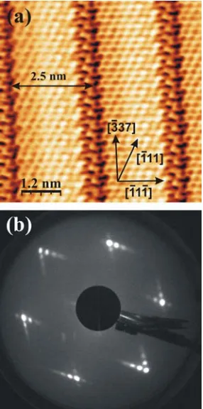
Figure 1 Low-temperature STM image of the WO2/W(110)
surface: Vsample = –0.06 V, It = 0.10 nA, size 6.5 nm × 6.5
nm, 78 K (a). LEED pattern from the WO2/W(110) surface,
acquired at a primary beam energy of 70 eV (b).
High temperature oxidation of the W(110) surface leads to the formation of an ultrathin WO2 layer [50]. A typical STM image and a LEED pattern taken from the WO2/W(110)
surface are shown in Figs. 1a and 1b, respectively. The WO2 has an O–W–O trilayer structure
and forms well-ordered oxide nanorows on the surface, separated by 2.5 nm (Fig. 1a). These rows appear as bright regions with dark depressions in between. The LEED pattern (Fig. 1b) shows characteristic satellite spots around each primary W(110) spot, representing two equivalent overlayer domains on the surface. The WO2 nanorows follow either the [-337] or
the [-33-7] directions of the W(110) substrate depending on the domain [50]. The WO2
overlayer has an oblique unit cell with unit cell vectors a = 2.5 nm and b = 13.0 nm, as
can influence the self-assembly of C60 molecules, the WO2/W(110) surface represents an
interesting nanostructured template.
At a very low coverage (0.2 ML), C60 molecules start nucleating at the inner step edges
of the WO2/W(110) surface (see Fig. 2a), which provides evidence for a weak molecule–
substrate interaction and for the diffusion of the molecules on the surface at room temperature. C60 molecules appear as bright protrusions in the STM image and decorate
substrate’s inner step edges, forming molecular chains. The tungsten oxide nanorows of the underlying substrate are also visible (Fig. 2a). At intermediate coverage (0.4–0.7 ML), C60
molecules self-assemble at room temperature into compact two-dimensional islands with a hexagonal close packed structure (see Fig. 2b). The C60 molecular layer is incommensurate
with the WO2/W(110) substrate. However, the growth of the C60 overlayer starts from the
substrate’s inner step edges, which follow the [-111] direction on the surface. This behaviour causes one of the primary directions of the molecular layer to coincide with the [-111] direction of the WO2/W(110) surface. This is a clear indication that the substrate plays a
certain role in the adsorption and arrangement of the molecules. The angle between this direction of the C60 layer and the [-337] direction of the oxide nanorows is equal to 23°.
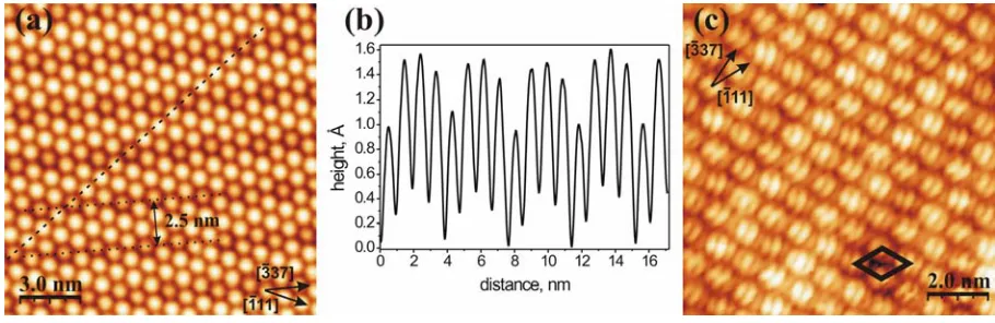
Figure 2 Low-temperature STM images acquired after the deposition of 0.2 ML (a), 0.5 ML (b) and 1 ML (c)
of C60 molecules onto the WO2/W(110) surface. (a) Vsample = +1.0 V, It = 0.10 nA, size 76 nm × 76 nm, 78 K.
(b) Vsample = +1.0 V, It = 0.10 nA, size 200 nm × 200 nm, 78 K. (c) Vsample = –1.5 V, It = 0.13 nA, size 15.4 nm
× 15.4 nm, 78 K. The unit cell of the C60 lattice is shown in black (c) and has the following parameters: the unit
cell vectors are each equal to 0.95 nm ± 0.05 nm, and the angle between them is 60º ± 0.5º.
The intermolecular bonding that occurs through the C60 π-electron system (π–π
stacking) appears to be stronger than the molecule–substrate interaction, leading to the formation of such compact islands. This is confirmed by the fact that there are no single C60
molecules adsorbed in the middle of substrate terraces after deposition, indicating a high mobility of the individual molecules on the surface at room temperature. Furthermore, each WO2/W(110) substrate terrace is covered with a single molecular domain, with terrace widths
of up to 40 nm, and domain boundaries are rarely observed. The distribution of the C60
among the substrate terraces is not homogeneous at this coverage - some terraces have almost no C60. This indicates that C60 molecules can easily cross substrate step edges while moving
on the surface as a result of interterrace diffusion.
At approximately 1 ML coverage, the molecules form large domains whose width is limited only by the width of the WO2/W(110) substrate terraces. One molecular monolayer is
defined as the case in which the substrate is completely covered by C60 molecules such that if
one further molecule is added, it will have no direct contact with the substrate and will form a second layer. For the C60 monolayer on the WO2/W(110) surface, the molecular packing
density is 1.25 C60 molecules per 1 nm2. The unit cell of the C60 lattice (shown in black in
are each equal to 0.95 nm ± 0.05 nm, and the angle between them is 60° ± 0.5°, forming a hexagonal close packed structure. The intermolecular separation within the overlayer is very close to the natural molecule–molecule distance of 1 nm observed in bulk C60 crystals. The
formation of ordered domains of such an extent and the C60–C60 separation further indicate
the presence of a significant intermolecular interaction, as well as a low diffusion barrier for the molecules on the WO2/W(110) surface at room temperature. Thus, C60 molecules are
[image:5.595.73.528.190.338.2]physisorbed on this surface and a weak molecule–substrate interaction occurs through the molecular π-electron system.
Figure 3 Low-temperature STM image of C60 on the WO2/W(110) surface, showing chains of the ‘dim’
molecules, which occupy the grooves between the oxide nanorows of the WO2/W(110) surface: Vsample = –0.7
V, It = 0.3 nA, size 15.6 nm × 15.6 nm, 78 K (a). Dotted lines indicate the [-337] direction of the nanorows. A
line profile (along the dashed line in Fig. 3a) indicating the height difference between the ‘bright’ and ‘dim’ C60
(b). Low-temperature STM image of C60 on the WO2/W(110) surface, showing that the C60 molecules are
oriented in one direction at 78 K: Vsample = +0.9 V, It = 0.70 nA, size 10 nm × 10 nm, 78 K (c). The unit cell of
the C60 overlayer is shown in black.
At some voltage biases, the C60 molecules on the WO2/W(110) surface show a
significant difference in apparent height (see Fig. 3a), which can be a reflection of local electronic and/or topographic variations. These so called ‘bright’ and ‘dim’ molecules have been previously observed by STM on a variety of surfaces and attributed to C60-induced
substrate reconstructions [22, 28, 30–36]. Such surface reconstructions can lead to two topographically different C60 adsorption sites, where ‘dim’ C60 molecules are sunk into
nanopits of the reconstructed substrate, and are lower in height than ‘bright’ ones. Other explanations suggest that this apparent height difference is due to electronic and molecular orientation effects [56, 57]. From Fig. 3a it is clearly seen that the ‘dim’ C60 molecules on the
WO2/W(110) are arranged in dark chain-like structures. The distance between these chains is
equal to 2.5 nm, as observed by STM. From STM images it is clear that the ‘dim’ C60
molecules follow the oxide nanorows of the substrate and are adsorbed between them. The nanostructured WO2/W(110) surface exhibits grooves separated by 2.5 nm [50], which are
seen as dark depressions in the STM image (Fig. 1a). The ‘dim’ C60 molecules observed in
Fig. 3a occupy these grooves, and are situated slightly lower than the others (‘bright’ C60).
The line profile shown in Fig. 3b indicates that the height difference between the ‘bright’ and ‘dim’ C60 molecules is equal to approximately 0.6 Å. The same value of corrugation was
observed for oxide nanorows forming the WO2/W(110) surface [50], indicating that such an
apparent height difference between C60 molecules is due to the substrate topography.
Furthermore, the similar apparent height difference (in the range 0.4–1.0 Å) has been observed between the ‘bright’ and ‘dim’ C60 molecules on other surfaces and was explained
electron orbitals of the ‘dim’ C60 molecules, caused by their specific arrangement on the
surface, which results in proximity of the molecule to the W layer.
Low-temperature STM of C60 molecules performed at 78 K demonstrates well-resolved
molecular orbitals within individual molecules. It was not possible to resolve these orbitals by performing STM at room temperature. This is most likely due to movement (rotation) of the molecules within the layer at this temperature. At 78 K however, most of the molecules in the complete C60 monolayer on the WO2/W(110) surface are aligned in one direction due to the
molecule–substrate interaction and the suppressed movement of the molecules at such a low temperature. This is shown in Fig. 3c by the ordered molecular orbitals (lobes) of individual C60. The molecules appear on the STM image as spheres composed of three ‘stripes’
(molecular lobes), suggesting that the same part of each C60 molecule is facing the substrate.
The parallel orientation of the C60 on the WO2/W(110) surface indicates that the molecule–
substrate interaction is strong enough to align the molecules at low temperature, when their movement is suppressed. Similar parallel orientation of the C60 molecules has been
previously observed on certain other surfaces by low-temperature STM [25, 26, 28, 32, 33].It is noted that STM images exhibiting three molecular lobes within an individual C60 molecule
have been acquired at a sample bias in the range from +0.7 V to +1.0 V (+0.9 V in Fig. 3c). At such a voltage, electron tunnelling occurs into the lowest unoccupied molecular orbital (LUMO) of C60 (which will be shown later by STS analysis), making the LUMO responsible
for the ‘three-stripe’ appearance of C60 molecules on the WO2/W(110) surface. C60 molecules
exhibiting three ‘stripes’ have been previously observed by STM on different metal and semiconductor surfaces [22, 30, 31, 40, 58, 59]. In most of these cases the proposed C60
orientation was the one in which the carbon–carbon bond that forms the border between two adjacent hexagons of C60 is parallel to the substrate [30, 31, 40, 58, 59].
In order to define the orientation of C60 molecules on the WO2/W(110) surface, the ab
initio density of states (DOS) calculations were performed using the Vienna Ab initio Simulation Package (VASP) program. VASP implements a projected augmented basis set (PAW) [60] and periodic boundary conditions. The electron exchange and correlation was simulated by local density approximation (LDA) pseudopotentials with a Ceperley–Alder exchange-correlation density functional [61]. A Γ-centred (2 × 2 × 1) k-point grid was used for all calculations to sample the Brillouin zone. The applied energy cut-off was 400 eV. For the DOS a smearing of 0.2 eV was applied using the Methfessel–Paxton method [62]. The global break condition for the electronic self-consistent loops was set to a total energy change of less than 1×10⁻⁴ eV. To find the optimum surface site of a single C60 molecule on one O–
W–O layer of WO2, five different surface sites were sampled and the total energy of those
systems was calculated. To minimize the energy of the system, different orientations of C60
on the surface were simulated. For all orientations the C60 molecule was allowed to relax on a
constrained layer of WO2. The partial charge density of these systems was calculated in a
range from Ef to 1 eV, where Ef is the Fermi energy. This partial charge density was then
compared with the experimental STM images.
The molecular orientation in which the carbon–carbon bond that forms the border between two adjacent hexagons of C60 is parallel to the WO2/W(110) surface (h–h
orientation) was found to have the lowest energy of all other orientations under consideration. The proposed model for the C60 overlayer on the WO2/W(110) surface is shown in Fig. 4.
The partial charge density of the h–h orientation indicates three distinct ‘stripes’ as the inner structure of the C60 molecule (see Fig. 4, inset). This simulated inner structure is in good
agreement with the lobe-resolved experimental STM images of C60, suggesting that the h–h
orientation is the most energetically favourable orientation of the C60 molecule on the
Figure 4 Schematic representation of the C60 overlayer
on the WO2/W(110) surface. The C atoms of C60 are
denoted by black spheres; the O and the W atoms of the oxide layer are denoted by red and green spheres, respectively. The inset shows the partial charge density of the individual C60 with the h–h orientation on the
[image:7.595.316.507.74.328.2]surface.
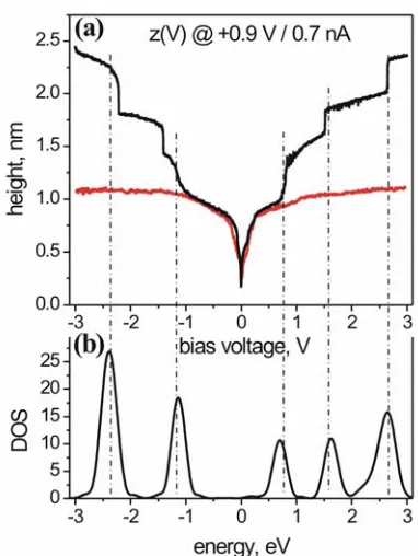
Figure 5 z(V) spectra recorded at 78 K from 1
ML of C60 on the WO2/W(110) surface (black
curve) and from the clean WO2/W(110) surface
(red curve) (a). The calculated DOS for the C60 in
the h–h orientation on the WO2/W(110) surface
(b).
Figure 5 shows a comparison between the z(V) spectrum recorded at a temperature of 78 K from the C60 overlayer on the WO2/W(110) surface and the result of DFT calculations
for the h–h orientation of C60. It is important to note that z(V) spectroscopy is an STM-based
technique providing information on the density of states of the material, which is probed as a function of voltage (sample bias) through changes in the tip height [5, 9]. The z(V) spectrum was recorded at 78 K over an individual C60 molecule within the image shown in Fig. 3c and
provides averaged information about electronic structure of the molecule. The spectrum in Fig. 5a shows five prominent features: the two steps observed at –2.3 V and –1.2 V and the three steps observed at +0.7 V, +1.6 V and +2.7 V are related to occupied and unoccupied states, respectively. These characteristic steps are seen due to the increasing number of new channels (molecular orbitals) available for tunnelling as the bias voltage increases. These features are absent on the z(V) curve obtained from the clean WO2/W(110) surface, which
proves that they are associated with the C60. Furthermore, the z(V) spectrum in Fig. 5a shows
good correlation with the density of states (DOS) obtained by DFT calculation (Fig. 5b). For the C60 on the WO2/W(110) surface, the LUMO is located at +0.7 eV and the highest
occupied molecular orbital (HOMO) at –1.2 eV. It is noted that the C60 molecules exhibit
three distinct ‘stripes’ (molecular lobes) on STM images, when electron tunnelling occurs into the LUMO (see Fig. 3c). The HOMO–LUMO band gap of the C60 on the WO2/W(110)
surface obtained from STS data is equal to 1.9 eV, which is in excellent agreement with previous STS measurements of C60 on surfaces with low reactivity [25–30, 54, 55] and
theoretical calculations [54, 55, 63, 64].
The self-assembly of C60 molecules on the WO2/W(110) surface has been investigated
by low-temperature STM/STS, LEED and DFT calculations. A well-ordered molecular layer was obtained in which the C60 molecules form a close-packed hexagonal structure with a unit
cell parameter equal to 0.95 nm. The nucleation of the C60 layer starts at the substrate’s inner
step edges. Low-temperature STM of C60 molecules performed at 78 K demonstrates
well-resolved molecular orbitals within individual molecules. Within the C60 monolayer on the
WO2/W(110) substrate at a temperature of 78 K, the molecules have the h–h orientation on
the surface and are aligned in one direction due to intermolecular interaction, as shown by the ordered molecular orbitals of individual C60. STS data obtained from the C60 monolayer on
the WO2/W(110) surface are in good agreement with DFT calculations. By using the
WO2/W(110) surface as a preformed nanostructured template, it was shown that the ‘dim’ C60
molecules follow the oxide nanorows of the substrate, occupy the grooves between them, and, as a result, are situated slightly lower than the others (‘bright’ C60).
Acknowledgements
This work was supported by Science Foundation Ireland (Principal Investigator grant number 00/PI.1/C042 and Walton Visitor Award grant number 08/W.1/B2583) and by Program of Presidium of Russian Academy of Sciences. STM topographic images were processed using WSxM software [65].
References
[1] Barth, J. V. Ann. Rev. Phys. Chem.2007, 58, 375–407.
[2] Barth, J. V.; Costantini, G.; Kern, K. Nature2005, 437, 671–679.
[3] Barlow, S. M.; Raval, R. Surf. Sci. Rep.2003, 50, 201–341.
[4] Rosei, F.; Schunack, M.; Naitoh, Y.; Jiang, P.; Gourdon, A.; Lægsgaard, E.; Stensgaard, I.; Joachim, C.; Besenbacher, F. Prog. Surf. Sci.2003, 71, 95–146.
[5] Krasnikov, S. A.; Sergeeva, N. N.; Sergeeva, Y. N.; Senge, M. O.; Cafolla, A. A. Phys. Chem. Chem. Phys.2010, 12, 6666–6671.
[6] Schnadt, J.; Xu, W.; Vang, R. T.; Knudsen, J.; Li, Z.; Lægsgaard, E.; Besenbacher, F.
Nano Res.2010, 3, 459–471.
[7] Krasnikov, S. A.; Beggan, J. P.; Sergeeva, N. N.; Senge, M. O.; Cafolla, A. A.
Nanotechnology2009, 20, 135301.
[8] Liang, H.; He, Y.; Ye, Y. C.; Xu, X. G.; Cheng, F.; Sun, W.; Shao, X.; Wang, Y. F.; Li, J. L.; Wu, K. Coord. Chem. Rev.2009, 253, 2959–2979.
[9] Beggan, J. P.; Krasnikov, S. A.; Sergeeva, N. N.; Senge, M. O.; Cafolla, A. A. J. Phys.: Condens. Matter2008, 20, 015003.
[10] Krasnikov, S. A.; Hanson, C. J.; Brougham, D. F.; Cafolla, A. A. J. Phys.: Condens. Matter2007, 19, 446005.
[11] van der Molen, S. J.; Liljeroth, P. J. Phys.: Condens. Matter 2010, 22, 133001.
[12] Fichou, D. J. Mater. Chem. 2000, 10, 571–588.
[13] Bonifazi, D.; Enger, O.; Diederich, F. Chem. Soc. Rev.2007, 36, 390–414.
[14] Xenogiannopoulou, E.; Medved, M.; Iliopoulos, K.; Couris, S.; Papadopoulos, M. G.; Bonifazi, D.; Sooambar, C.; Mateo-Alonso, A.; Prato, M. ChemPhysChem 2007, 8,
1056–1064.
[15] Park, H.; Park, J.; Lim, A. K. L.; Anderson, E. H.; Alivisatos, A. P.; McEuen, P. L.
Nature2000, 407, 57–60.
[16] Hebard, A. F.; Rosseinsky, M. J.; Haddon, R. C.; Murphy, D. W.; Glarum, S. H.; Palstra, T. T. M.; Ramirez, A. P.; Kortan, A. R. Nature1991, 350, 600–601.
[17] Tanigaki, K.; Ebbesen, T. W.; Saito, S.; Mizuki, J.; Tsai, J. S.; Kubo, Y.; Kuroshima, S.
[18] Nakaya, M.; Tsukamoto, S.; Kuwahara, Y.; Aono, M.; Nakayama, T. Adv. Mater.2010, 22, 1622–1625.
[19] Joachim, C.; Gimzewski, J. K.; Aviram, A. Nature2000, 408, 541–548.
[20] Hiorns, R.C.; Cloutet, E.; Ibarboure, E.; Vignau, L.; Lemaitre, N.; Guillerez, S.; Absalon, C.; Cramail, H. Macromolecules2009, 42, 3549–3558.
[21] Zhang, X.; Tang, L.; Guo, Q. J. Phys. Chem. C2010, 114, 6433–6439.
[22] Gardener, J. A.; Briggs, G. A. D.; Castell, M. R. Phys. Rev. B2009, 80, 235434.
[23] Diaconescu, B.; Yang, T.; Berber, S.; Jazdzyk, M.; Miller, G. P.; Tománek, D.; Pohl, K. Phys. Rev. Lett.2009, 102, 056102.
[24] Li, H. I.; Franke, K. J.; Pascual, J. I.; Bruch, L. W.; Diehl, R. D. Phys. Rev. B2009, 80,
085415.
[25] Grobis, M.; Yamachika, R.; Wachowiak, A.; Lu, X.; Crommie, M. F. Phys. Rev. B 2009, 80, 073410.
[26] Zhang, X.; He, W.; Zhao, A.; Li, H.; Chen, L.; Pai, W. W.; Hou, J.; Loy, M. M. T.; Yang, J.; Xiao, X. Phys. Rev. B2007, 75, 235444.
[27] Rogero, C.; Pascual, J. I.; Gómez-Herrero, J., Baró, A. M. J. Chem. Phys. 2002, 116,
832–836.
[28] Grobis, M.; Lu, X.; Crommie, M. F. Phys. Rev. B2002, 66, 161408.
[29] Schulze, G.; Franke, K. J.; Pascual, J. I. New J. Phys.2008, 10, 065005.
[30] Schull, G.; Néel, N.; Becker, M.; Kröger, J.; Berndt, R. New J. Phys.2008, 10, 065012.
[31] Schull, G.; Berndt, R. Phys. Rev. Lett.2007, 99, 226105.
[32] Pai, W. W.; Hsu, C.-L.; Lin, M. C.; Lin, K. C.; Tang, T. B. Phys. Rev. B 2004, 69,
125405.
[33] Abel, M.; Dmitriev, A.; Fasel, R.; Lin, N.; Barth, J. V.; Kern, K. Phys. Rev. B2003, 67,
245407.
[34] Hsu, C.-L.; Pai, W. W. Phys. Rev. B2003, 68, 245414.
[35] Weckesser, J.; Cepek, C.; Fasel, R.; Barth, J. V.; Baumberger, F.; Greber, T.; Kern, K.
J. Chem. Phys.2001, 115, 9001–9009.
[36] Murray, P. W.; Pedersen, M. Ø.; Lægsgaard, E.; Stensgaard, I.; Besenbacher, F. Phys. Rev. B1997, 55, 9360.
[37] Li, Y. Z.; Patrin, J. C.; Chander, M.; Weaver, J. H.; Chibante, L. P. F.; Smalley, R. E.
Science1991, 252, 547–548.
[38] Li, Y. Z.; Chander, M.; Patrin, J. C.; Weaver, J. H.; Chibante, L. P. F.; Smalley, R. E.
Science1991, 253, 429–433.
[39] Hou, J. G.; Yang, J. L.; Wang, H. Q.; Li, Q. X.; Zeng, C. G.; Lin, H.; Bing, W.; Chen, D. M.; Zhu, Q. S. Phys. Rev. Lett.1999, 83, 3001–3004.
[40] Pascual, J. I.; Gómez-Herrero, J.; Rogero, C.; Baró, A. M.; Sánchez-Portal, D.; Artacho, E.; Ordejón, P.; Soler, J. M. Chem. Phys. Lett.2000, 321, 78–82.
[41] Dunn, A. W.; Svensson, E. D.; Dekker, C. Surf. Sci.2002, 498, 237–243.
[42] Lu, C.; Zhu, E.; Liu, Y.; Liu, Z.; Lu, Y.; He, J.; Yu, D.; Tian, Y.; Xu, B. J. Phys. Chem. C2010, 114, 3416–3421.
[43] Loske, F.; Bechstein, R.; Schütte, J.; Ostendorf, F.; Reichling, M.; Kühnle, A.
Nanotechnology2009, 20, 065606.
[44] Carvalho, A. J. P.; Ramalho, J. P. P. Appl. Surf. Sci.2010, 256, 5365–5369.
[45] Nilius, N. Surf. Sci. Rep.2009, 64, 595–659.
[46] Henrich, V. E.; Cox, P. A. The Surface Science of Metal Oxides; Cambridge University
Press: Cambridge, 1994.
[47] Noguera, C. Physics and Chemistry of Oxide Surfaces; Cambridge University Press:
Cambridge, 1996.
A. B.; Krasnikov, S. A.; Kleimenov, E. Y.; Nesterov, M. A.; Rüdiger, U.; et al. Phys. Rev. B2005, 72, 060401.
[49] Krasnikov, S. A.; Vinogradov, A. S.; Hallmeier, K.-H.; Höhne, R.; Ziese, M.; Esquinazi, P.; Chassé, T.; Szargan, R. Mater. Sci. Eng. B2004, 109, 207–212.
[50] Radican, K.; Bozhko, S. I.; Vadapoo, S.-R.; Ulucan, S.; Wu, H.-C.; McCoy, A.; Shvets, I. V. Surf. Sci.2010, 604, 1548–1551.
[51] Krasnikov, S. A.; Murphy, S.; Berdunov, N.; McCoy, A. P.; Radican, K.; Shvets, I. V.
Nanotechnology2010, 21, 335301.
[52] Radican, K.; Berdunov, N.; Shvets, I. V. Phys. Rev. B2008, 77, 085417.
[53] Radican, K.; Berdunov, Manai, G.; N.; Shvets, I. V. Phys. Rev. B2007, 75, 155434.
[54] Lu, X.; Grobis, M.; Khoo, K. H.; Louie, S. G.; Crommie, M. F. Phys. Rev. B 2004, 70,
115418.
[55] Lu, X.; Grobis, M.; Khoo, K. H.; Louie, S. G.; Crommie, M. F. Phys. Rev. Lett. 2003, 90, 096802.
[56] Giudice, E.; Magnano, E.; Rusponi, S.; Boragno, C.; Valbusa, U. Surf. Sci.1998, 405,
L561–L565.
[57] Altman, E. I.; Colton, R. J. Phys. Rev. B1993, 48, 18244.
[58] Tsukamoto, S.; Nakayama, T.; Aono, M. Carbon2007, 45, 1261–1266.
[59] Nakaya, M.; Kuwahara, Y.; Aono, M.; Nakayama, T. Small2008, 4, 538–541.
[60] Kresse, G.; Furthmüller, J. Phys. Rev. B1996, 54, 11169–11186.
[61] Ceperley, D. M.; Alder, B. J. Phys. Rev. Lett.1980, 45, 566–569.
[62] Methfessel, M.; Paxton, A. T. Phys. Rev. B1989, 40, 3616–3621.
[63] Sau, J. D.; Neaton, J. B.; Choi, H. J.; Louie, S. G.; Cohen, M. L. Phys. Rev. Lett.2008, 101, 026804.
[64] Rivelino, R.; de Brito Mota, F. Nano Lett.2007, 7, 1526–1531.