Characterization of Ferroelectric Na
xK
1 xNbO
3System Films Prepared
by Pulsed Laser Deposition
Fengping Lai
1, Rong Tu
1, Takashi Goto
1and Jingfeng Li
21
Institute for Materials Research, Tohoku University, Sendai 980-8577, Japan
2State Key Laboratory of New Ceramics and Fine Processing, Department of Materials Science and Engineering,
Tsinghua University, Beijing 100084, P. R. China
Ferroelectric NaxK1xNbO3(NKN) films were prepared on quartz and Pt/SrTiO3(100) substrates by pulsed laser deposition. The effects of
composition and preparation conditions on the crystal structure and ferroelectricity of the NKN films were investigated by changing the Na content (x), substrate temperature (Tsub), oxygen partial pressure (PO2), target-to-substrate distance (Dt-s) and laser energy density (EL). The
permittivity values of the NKN films were 390 to 520 at room temperature and 100 kHz, showing a maximum atx¼0:5. The maximum remnant polarization value was8:2102C m2atx¼0:5. [doi:10.2320/matertrans.MRA2008116]
(Received April 8, 2008; Accepted June 5, 2008; Published July 16, 2008)
Keywords: sodium potassium niobate film, pulse laser deposition, ferroelectricity
1. Introduction
The NaNbO3-KNbO3solid solution system is a promising
lead-free ferroelectric and piezoelectric material and thus great effort has been made to increase its ferroelectric and
piezoelectric performance.1,2) According to the phase
dia-gram for the solid solution of the NaxK1xNbO3 (NKN)
system, a morphotropic phase boundary (MPB) separating two orthorhombic ferroelectric phases exists at anxof around 0.5.3)Near this MPB composition, the dielectric constant and piezoelectric constant are the highest4,5) with the smallest coercive field (Ec).6)Saitoet al.reported that Na0:5K0:5NbO3
-based sintered bodies had a large piezoelectric coefficient
(d33), with a comparable value to that of commercial
Pb(Zr,Ti)O3 (PZT).7,8)
NKN and NKN-based thin films have potential applica-tions for non-volatile ferroelectric random access memories (FRAM) and ferroelectric actuators and devices in micro-electromechanical system (MEMS). Na0:5K0:5NbO3 films
have been prepared by several routes, including pulsed laser deposition (PLD),9,10)magnetron sputtering,11,12)
metal-organic chemical vapor deposition (MOCVD)13,14) and
sol-gel.15,16)
Pulsed laser deposition has been widely applied for preparation of many kinds of thin films due to several advantages, i.e., stoichiometric transfer of compositions from source to film, growth from a high energy beam resulting in high crystallinity and inherent simplicity for the growth of multilayered structures.17) Na
0:5K0:5NbO3 thin films were
first prepared by Choet al.using pulsed laser deposition.18) Kimet al.prepared a highly oriented Na0:5K0:5NbO3film by
pulsed laser deposition, the piezoelectric constant of which was comparable to that of epitaxially grown PZT film by pulsed laser deposition.19)
However, no study on NKN films with various composi-tions has been reported. In this work, NKN films were prepared by pulsed laser deposition, and the effects of preparation conditions on the crystal structure and the electrical properties of the films were investigated.
2. Experimental
Starting materials of Na2CO3, K2CO3and Nb2O5powders
were mixed in the nominal composition of NaxK1xNbO3
with x changing from 0.2 to 0.8, pressed into pellets with
diameter () of 15 mm and height (H) of 3 mm and then
calcined at 1173 K for 14.4 ks. The pellets were sintered by spark plasma sintering (SPS) at 1323 K forx¼0:2to 0.6 and at 1373 K forx¼0:8for 600 s in a vacuum and then annealed at 1123 K for 36 ks in air.
NKN films were prepared on quartz glass and Pt/ SrTiO3(100) substrates by pulsed laser deposition. Hereafter,
various compositions of NKN films are expressed asxNKN,
wherexrepresents the nominal composition (NaxK1xNbO3)
of the targets. A third harmonic wavelength of a Q-switch pulsed Nd:YAG laser (Spectron Laser System SL805,
¼355nm, pulse duration of 15 ns and repetition of
10 Hz) was used as the laser source. Deposition parameters are summarized in Table 1.
Amorphous quartz plates (12100:5mm) and
SrTiO3(100) single crystal wafers (10100:5mm) with
a Pt bottom electrode were used as substrates. The target and substrate stage were rotated at 12 rpm in converse directions.
Films were deposited at a vacuum (107Pa) and different
[image:1.595.305.550.667.786.2]oxygen partial pressures (PO2) ranging from 2.67 to 26.7 Pa.
Table 1 Deposition parameters for NKN films prepared by pulsed laser deposition.
Targets NKN pellets
(x¼0:2to 0.8,15 mm,H3 mm)
Substrate Quartz glass, STO (100) single crystal
Substrate temperature (Tsub) 723–973 K
Deposition ambient Vacuum (10
7Pa)
Oxygen partial pressure,PO2(2.67–26.7 Pa)
Distance between target and
substrates (Dt-s) 40–70 mm
Laser energy density (EL) 2{7:5104J m2
Deposition time 3.6–14.4 ks
The substrate temperature (Tsub) was changed from 723 to 973 K. The distance between the target and the substrate
(Dt-s) was changed stepwise from 45 to 70 mm. The power
density of the laser output (EL) was controlled in a range from 2 to7:5104J m2.
The crystal structure was examined by X-ray diffraction (Rigaku, RAD-2C). To determine the lattice constants of the targets and the films, X-ray step scanning was employed. The thickness was measured by a profilemeter (Taylor-Hobson Talystep). The composition was studied by electron probe microanalysis (EPMA, JEOL JXA-8621MX). The surface morphology was observed by scanning electron microscopy (SEM, Hitachi S-3100H). The dielectric properties were measured in air by an AC impedance analyzer (Hewlett Packard 4194) in a frequency (f) range of102to107Hz from room temperature to 773 K. The polarization–electric field (P–E) hysteresis loops were measured by a ferroelectric test
system (FCE-1, TOYO Corp., Japan) at a frequency (f) of
10 kHz at room temperature.
[image:2.595.60.279.522.746.2]3. Results and Discussion
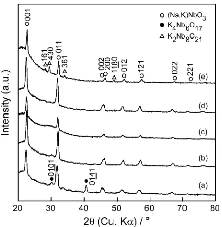
Figure 1 shows the effect of x on the XRD patterns of
NKN films atPO2¼10Pa,Tsub¼973K,Dt-s¼60mm and
EL ¼3:8104J m2 for 7.2 ks. Perovskite structures were obtained in NKN films with different compositions, which
were the powder diffraction of KNbO3 (JCPDS #32-0822)
and NaNbO3(JCPDS #33-1270). A small amount of second
phases of K4Nb6O17 (Orthorhombic, a¼0:783,b¼3:321
andc¼0:646nm) and K2Nb8O21(Orthorhombic,a¼1:25,
b¼3:75 andc¼0:396nm) was contained at 0.2NKN and
0.8NKN, respectively. The NaNbO3-KNbO3 system is a
pseudo-binary solid solution system in the whole range and all targets were of perovskite structure in a single phase. Second phases observed in the NKN films near the two end members could have been caused by the volatilization
of Na and K, which is a common problem encountered in the preparation of compounds containing alkali metal elements.20,21) In addition, slight changes in stoichiometry (both on the Na-rich and the K-rich side) easily lead to the formation of second phases.22)
NKN films with different compositions had similar dense microstructures with particulates, showing little dependence on composition.
The average compositions of NKN films measured by EPMA were almost in agreement with that of the targets. The difference of Na/(Na+K) and (Na+K)/Nb ratios between the NKN films and targets was less than 10%.
The structure of NaNbO3 and KNbO3 crystals is
ortho-rhombic at RT with lattice parameters of a¼0:5568nm,
b¼1:552nm and c¼0:5504nm, and a¼0:5695nm, b¼
0:5721nm and c¼0:3973nm, respectively. To compare
lattice parameters between NKN films and bulk crystals, the lattice parameters were transformed into a pseudo-cubic structure through relations of ac¼a=
ffiffiffi 2 p
, bc¼b=
ffiffiffi 2 p
and
cc¼c.23) Figure 2 depicts the pseudo-cubic lattice
param-eters of the NKN targets and films prepared atTsub¼973K
and PO2¼10Pa for 7.2 ks on quartz glass substrates. The
lattice parameters of both targets and NKN films decreased with increasing Na content. A transition of slope in lattice parameters occurred at x¼0:4 to 0.6 for both targets and
films, owing to the MPB composition of NaNbO3–KNbO3
system. The lattice parameters of the NKN films were smaller than those of the targets, which might have been due to compressive stress generated during the pulsed laser deposition and/or cooling process. Film compressive stress has been reported to arise due to a variety of different mechanisms, including differential thermal contraction, island coalescence, grain growth, grain boundary diffusion, competitive columnar growth and high-energy particle
bombardment.24) Since the thermal expansion coefficient
of quartz is smaller than that of NKN films, the smaller lattice parameters of NKN films can not be explained by the difference in thermal expansion, but may result from
Fig. 1 Effect ofxon XRD patterns of NKN films deposited on quartz glass at x¼0:2 (a), 0.4 (b), 0.5 (c), 0.6 (d) and 0.8 (e) at Tsub¼973K,
PO2¼10Pa,Dt-s¼60mm andEL¼3:810
4Jm2for 7.2 ks.
Fig. 2 Effect ofxon the pseudo-cubic lattice parametersac,bcandccof the NKN targets and films (subscript c means pseudo-cubic).
[image:2.595.315.535.550.757.2]the stress generated during the pulsed laser deposition process. Some stoichiometric deviation or defects in the NKN films may also be associated with the smaller lattice parameters.25)
The effect of deposition parameters, such as Tsub, PO2, Dt-s and EL, on the crystal structure and microstructure of
NKN films will be described later, taking x¼0:5 as an
example.
Figure 3 shows the effect ofTsub on the XRD patterns of
0.5NKN films prepared at PO2¼10Pa, Dt-s¼50mm and
EL ¼3:8104J m2 for 3.6 ks. A perovskite structure of
0.5NKN film was identified at each Tsub. The (001) peak
of 0.5NKN film became significant with increasing Tsub,
showing (001) orientational growth. A small amount of
the second phase of K4Nb6O17 was detected at Tsub¼923 and 973 K.
Figure 4 shows the effect of Tsub on the microstructure
of 0.5NKN films. The 0.5NKN film showed a micro-sized particulate microstructure with a relative flat matrix at
Tsub ¼723K and a dense particulate microstructure at
Tsub ¼973K. The stacking density of the particulates
increased with increasing Tsub, which was associated with
decreasing particulate size. This indicates that the adhesion between the substrate and the ablated species increased at
higher Tsub. There was no obvious existence of a second
phase at highTsubfrom surface morphology observation.
Figure 5 shows the effect ofPO2 on the XRD patterns of
the 0.5NKN films prepared at Tsub¼923K, Dt-s¼50mm
Fig. 3 Effect ofTsubon XRD patterns of 0.5NKN films prepared on quartz glass atTsub¼723(a), 873 (b), 923 (c) and 973 K (d) atPO2¼10Pa,Dt-s
of 50 mm andEL¼3:8104J m2for 3.6 ks.
Fig. 4 Effect ofTsubon microstructures of 0.5NKN films prepared on quartz glass atTsub¼723(a) and 973 K (b) atPO2¼10Pa,
Dt-s¼50mm andEL¼3:8104J m2for 3.6 ks.
Fig. 5 Effect ofPO2on XRD patterns of 0.5NKN films prepared on quartz
glass at vacuum (a),PO2¼2:67(b), 10 (c) and 26.7 Pa (d) atTsub¼973K,
[image:3.595.60.279.69.297.2] [image:3.595.314.535.71.296.2] [image:3.595.67.531.360.576.2]andEL¼3:8104J m2for 3.6 ks. In a vacuum (P¼107
Pa), a small amount of the second phase of K4Nb6O17
appeared. The peaks of K4Nb6O17 and 0.5NKN films
decreased with increasing PO2. The intensity ratio of (001)
to (011) of 0.5NKN film (INKN-001=INKN-011) increased from 2.1 in a vacuum to 5.3 atPO2¼26:7Pa, while it was 0.67 for
the 0.5NKN target. This implies that the (001) orientation of 0.5NKN films is preferred at higherPO2. A similar effect of PO2 on the preferred orientation of Na0:5K0:5NbO3films has
been reported for Pt80Ir20 and SiO2(native oxide)/Si(111)
substrates by Cho et al.10)In their work, second phases of K2Nb8O21 and K2Nb4O11 were identified at PO2¼1:33Pa.
The formation of alkaline-poor niobates by pulsed laser deposition at a lowPO2may be caused by the high volatility
of Na and K. At highPO2 (53:2Pa), the present 0.5NKN
films were in a single phase and were highly (001)-oriented
(INKN-001=INKN-011¼60), showing a tendency similar to that
reported by Choet al.10)
Figure 6 shows the effect ofDt-s on the XRD patterns of
0.5NKN films prepared at 973 K, PO2¼10Pa and EL¼
3:8104J m2. The intensities of the second phase
(K4Nb6O17) and perovskite 0.5NKN film decreased with
increasingDt-s. A moderate distance and a longer deposition time were appropriate to obtain 0.5NKN films.
The microstructures of 0.5NKN films did not show much
difference under different PO2 and Dt-s, except for a
decreasing stacking density of the particulates. The specific effects ofPO2andDt-swere interrelated. The more collisions
which occurred between the laser-produced plume and the background gas, the lower the number of ablated species which arrived at the surface of substrates.
Figure 7 shows the effect of EL on the surface
micro-structure of 0.5NKN films prepared atTsub¼973K,PO2¼
10Pa andDt-s¼50mm. 0.5NKN films had a dense
micro-structure with particulates at EL¼5104J m2 and a
granular microstructure with micron-sized particulates at
EL ¼3:8104J m2. The amount of particulates decreased significantly with decreasingEL. AtEL <2:5104J m2, a dense microstructure with a grain size of 500 nm and a few particulates were observed. The deposition rates of 0.5NKN
films dramatically decreased from about 1.4 to 0:07
1010m s1 with decreasing E
L from 5 to 2104J m2. Moreover, the XRD patterns of 0.5NKN films turned to be
amorphous whenEL decreased to2104J m2, partly due
to the slow deposition rate.Dt-s of 40 mm andEL of 2:5
104J m2 were found to be effective to achieve an
in-crease in the deposition rate to0:61010m s1with clear
perovskite XRD peaks and only slight particulate generation, as shown in Fig. 7(d).
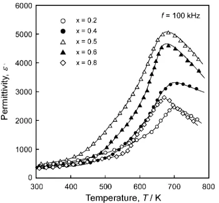
Figure 8 shows the temperature dependence of permit-tivity at 100 kHz for NKN films prepared on a Pt/STO(100)
substrate at Tsub¼973K, PO2¼10Pa and Dt-s¼60mm
for 7.2 ks. The permittivity continuously increased with increasing temperature and exhibited peaks around 680 K. The Curie temperature (Tc) slightly increased from 670 to
700 K with decreasing xfrom 0.8 to 0.2, slightly less than
those of sintered bodies reported by Egerton et al.19) The
permittivity peak value of 5000 was obtained for 0.5NKN films, which was larger than those of 1200 and 2500 for Na0:5K0:5NbO3 films prepared by Khartsevet al.using
RF-sputtering and pulsed laser deposition, respectively.26)The permittivity value of 5000 obtained in the present study is the highest thus far reported in the literature.
Figure 9 shows the hysteresis loops of NKN films prepared
on Pt/STO (100) substrates at Tsub¼973K, PO2 ¼10Pa
and Dt-s ¼60mm for 7.2 ks. Well-saturated hysteresis
loops were observed at f ¼10kHz under an electrical
field of 5106V m1 at room temperature. The remnant
polarization (Pr) reached the highest value of 8:2
102C m2 for 0.5NKN. The coercive field (E
c) of NKN
films varied from 1.24 to 1:57106V m1. The value of
Ec was the highest at 0.6NKN, with a slight dependence
on the composition. TheseEcvalues were smaller than that
of2106V m1of the c-axis-oriented NKN films prepared
by Choet al.10)
Figure 10 demonstrates the permittivity ("0) and remnant
polarization (Pr) of NKN films as a function of Na content at
room temperature. The "0 of NKN films at f ¼100kHz
ranged from 390 to 520 and showed the maximum value in 0.5NKN film. The permittivity of NKN films had a composi-tional dependence similar to that of NKN ceramics. The
peak permittivity of NKN ceramics was observed atx¼0:5
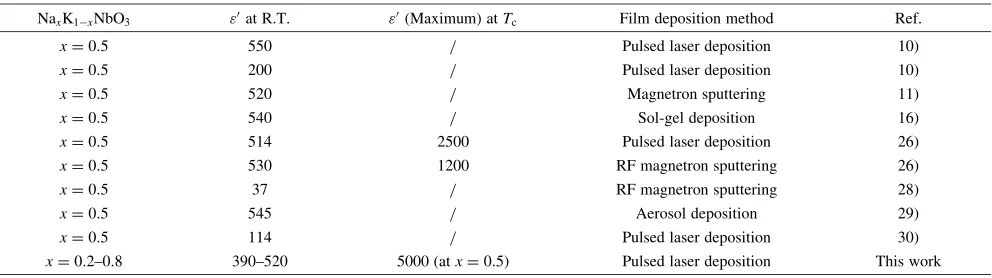
by Chuet al.27)and aroundx¼0:4to 0.6 by Zhanget al.5) Several groups have reported the permittivity of NKN films. Table 2 summarizes the permittivity of NKN films prepared by various processes, indicating rather small values of 37 by RF magnetron sputtering28)and 545 by aerosol deposition.29) High permittivity values above 500 have been reported for epitaxial and (001)-oriented 0.5NKN films,10,11)whereas the non-oriented 0.5NKN film in the present study showed a relatively high value. To date various compositions of NKN films have been prepared, but only the composition of 0.5NKN film has been focused on in the literature. This paper is the first to report the composition dependence of "0 and Pr, and the study herein reported achieved the highest"0of NKN film to date.
Fig. 6 Effect ofDt-son XRD patterns of 0.5NKN films prepared on quartz glass atDt-s¼50(a), 60 (b) and 70 mm (c) atTsub¼973K,PO2of 10 Pa
andEL¼3:8104J m2for 3.6 ks.
[image:4.595.61.281.71.294.2]Fig. 8 Temperature dependence of permittivity for NKN films prepared on Pt/STO(100) substrates atTsub¼973K,PO2¼10Pa andDt-s¼60mm
for 7.2 ks.
Fig. 9 Hysteresis loops of NKN films prepared on Pt/STO(100) substrates atTsub¼973K,PO2¼10Pa andDt-s¼60mm for 7.2 ks.
Fig. 7 Effect ofELon microstructures of 0.5NKN films prepared on quartz glass atEL¼5104J m2andDt-s¼60mm for 7.2 ks (a), 3:8104J m2andDt-s¼60mm for 3.6 ks (b),2104J m2andDt-s¼60mm for 30.4 ks (c) and2:5104J m2andDt-s¼40mm
[image:5.595.86.508.71.472.2] [image:5.595.60.281.542.747.2] [image:5.595.316.535.543.758.2]4. Conclusions
NKN films with different compositions were prepared by pulsed laser deposition. The compositions of the films were almost the same as those of the targets. The lattice parameters of the deposited films were smaller than those of the targets. The NKN films had a dense, uniform granular microstructure. HighTsub andPO2 promoted the (001) orientational growth.
EL was the key deposition parameter which controlled the
particulate generation on the film surface. Permittivity and remnant polarization showed the maximum values of 520 and
8:2102C m2at 0.5NKN, while the highest permittivity
value was 5000 atTc¼680K.
Acknowledgement
This research was partially supported by the Global COE Materials Integration Program, Tohoku University and the Japan Society for the Promotion of Science (JSPS), Asian CORE program ‘‘Interdisciplinary Science of Nanometers.’’
REFERENCES
1) K. Singh, V. Lingwal, S. C. Bhatt, N. S. Panwar and B. S. Semwal:
Mater. Res. Bull.36(2001) 2365–2374.
2) V. Lingwal, B. S. Semwal and N. S. Panwar: Bull. Mater. Sci.26
(2003) 619–625.
3) G. Shirane, R. Newnham and R. Pepinsky: Phys. Rev. 96 (1954) 581–588.
4) D. H. Cho, M. K. Ryu, S. S. Park, S. Y. Cho, J. G. Choi, M. S. Jang, J. P. Kim and C. R. Cho: J. Korean Phys. Soc.46(2005) 151–154. 5) B. P. Zhang, J. F. Li, K. Wang and H. L. Zhang: J. Am. Ceram. Soc.89
(2006) 1605–1609.
6) R. E. Jaeger and L. Egerton: J. Am. Ceram. Soc.45(1962) 209–213. 7) Y. Saito, H. Takao, T. Tani, T. Nonoyama, K. Takatori, T. Homma,
T. Nagaya and M. Nakamura: Nature432(2004) 84–87. 8) Y. Saito and H. Takao: Ferroelectrics338(2006) 1433–1448. 9) S. Abadei, S. Gevorgian, C.-R. Cho and A. Grishin: J. Appl. Phys.91
(2002) 2267–2276.
10) C.-R. Cho and A. Grishin: J. Appl. Phys.87(2000) 4439–2228. 11) M. Blomqvist, J. H. Koh, S. Khartsev, A. Grishin and J. Andreasson:
Appl. Phys. Lett.81(2002) 337–339.
12) H. J. Lee, C. W. Ahn, S. H. Kang, I. W. Kim, J. S. Lee and B. M. Jin: Ferroelectrics335(2006) 227–232.
13) C. R. Cho: Mater. Lett.57(2002) 781–786.
14) C. R. Cho and B. M. Moon: Integr. Ferroelectr.45(2002) 39–48. 15) F. Soderlind, P.-O. Kall and U. Helmersson: J. Cryst. Growth.281
(2005) 468–474.
16) Y. Nakashima, W. Sakamoto, H. Maiwa, T. Shimura and T. Yogo: Jpn. J. Appl. Phys. Part 246(2007) L311–L313.
17) M. N. R. Ashfold, F. Claeyssens, G. M. Fuge and S. J. Henley: Chem. Soc. Rev.33(2004) 23–31.
18) C.-R. Cho and A. Grishin: Appl. Phys. Lett.75(1999) 268–270. 19) J.-S. Kim, I. R. Hwang, S. H. Hong, J. H. Lee, B. H. Park, A. C. Woo
and N. Sahn: J. Korean Phys. Soc.48(2006) 1583–1587.
20) Y. T. Lu, X. M. Chen, D. Z. Jin and X. Hu: Mater. Res. Bull.40(2005) 1847–1855.
21) F. P. Lai and J. F. Li: J. Sol-Gel Sci. Technol.42(2007) 287–292.
22) A. Reisman and F. Holtzberg: J. Am. Ceram. Soc. 77 (1955)
2115–2119.
23) C. N. W. Darlington and H. D. Megaw: Acta Cryst. B29 (1973)
2171–2177.
24) P. R. Guduru, E. Chason and L. B. Freund: J. Mech. Phys. Solid.51
(2003) 2127–2148.
25) J. Bak-Misiuk, A. Misiuk, K. S. Zhuravlev, J. Z. Domagala, J. Adamczewska and V. V. Preobrazhenskii: Physica B308–310(2001) 820–822.
26) S. Khartsev, A. Grishin, J. Andreasson, J. H. Koh and J. S. Song: Integr. Ferroelectr.55(2003) 769–779.
27) S.-Y. Chu, W. Water, Y.-D. Juang and J.-T. Liaw: Ferroelectrics287
(2003) 23–33.
28) V. M. Kugler, F. Soderlind, D. Music, U. Helmersson, J. Andreasson and T. Lindback: J. Cryst. Growth254(2003) 400–404.
29) J. Ryu, J.-J. Choi, B.-D. Hahn, D.-S. Park, W.-H. Yoon and K.-H. Kim: Appl. Phys. Lett.90(2007) 152901.
[image:6.595.53.549.83.222.2]30) C. R. Cho, J. H. Koh, A. Grishin, S. Abadei and S. Gevorgian: Appl. Phys. Lett.76(2000) 1761–1763.
Fig. 10 Effect ofxon permittivity at 100 kHz and remnant polarization at room temperature of NKN films prepared on Pt/STO(100).
Table 2 Comparison of composition and permittivity values at 100 kHz of NKN films prepared by different methods.
NaxK1xNbO3 "0at R.T. "0(Maximum) atTc Film deposition method Ref.
x¼0:5 550 / Pulsed laser deposition 10)
x¼0:5 200 / Pulsed laser deposition 10)
x¼0:5 520 / Magnetron sputtering 11)
x¼0:5 540 / Sol-gel deposition 16)
x¼0:5 514 2500 Pulsed laser deposition 26)
x¼0:5 530 1200 RF magnetron sputtering 26)
x¼0:5 37 / RF magnetron sputtering 28)
x¼0:5 545 / Aerosol deposition 29)
x¼0:5 114 / Pulsed laser deposition 30)
x¼0:2{0:8 390–520 5000 (atx¼0:5) Pulsed laser deposition This work
[image:6.595.60.277.243.438.2]