Electromigration Behavior of through-Si-via (TSV) Interconnect
for 3-D Flip Chip Packaging
Sang-Su Ha
1, Jun-Mo Yang
2and Seung-Boo Jung
1;*1
School of Advanced Materials Science & Engineering, Sungkyunkwan University, 300 Cheoncheon-dong, Jangan-gu, Suwon 440-746, Korea
2National Nanofab Center, Measurement & Analysis, 53-3 Eoeun-dong, Yuseong-gu, Daejeon 305-806, Korea
The electromigration of conventional Sn-37Pb (in mass%) solder bumps was investigated with a current density of2:0104A/cm2at 393 K using three-dimensional (3-D) flip-chip specimens comprised of an upper Si chip and a lower FR-4 substrate. Electromigration failure of the Sn-37Pb solder bumps occurred with complete consumption of electroless Ni immersion Au (ENIG) under bump metallization (UBM) and void formation at the cathode side of the solder bump. Cross-sectional studies were conducted with scanning electron microscopy (SEM). Ni3Sn4intermetallic compound (IMC) layers were formed in both interfaces, while a typical eutectic structure of Pb- and Sn-rich phases was formed within the solder region. After 11 h current stressing, separation of the Pb- and Sn-rich phases occurred in the solder bump, while a void was formed in the cathode-side bump. After 18 h current stressing, the solder joints catastrophically failed due to the re-melting of the solder bump. [doi:10.2320/matertrans.M2009367]
(Received October 30, 2009; Accepted February 15, 2010; Published April 25, 2010)
Keywords: tin-lead, electromigration, through-Si-via (TSV), three-dimensional packaging
1. Introduction
Three-dimensional (3-D) flip chip stacking offers a variety of benefits compared with traditional wire-bonded pack-aging, including superior thermal and electrical performance, the highest input/output (I/O) capability, substrate flexibility for varying performance requirements, well established process equipment, expertise, proven construction, high reliability, and reduced form factors.1–3) Of these benefits,
the most valuable advantage for the recent trends of electronic products toward powerful multi-functionality and miniaturization, is the highest I/O capability. Because of this capability, the 3-D flip chip package has been widely adapted in the electronic industries. The reliability of the 3-D flip chip package has been extensively evaluated with temperature cycling, thermal shock treatment, high temperature curing and temperature-humidity storage testing.4–6) However, the
electrical property and reliability of the flip chip package remains poorly underatood.7–11)
The electromigration of solder joints under high current stressing is an important concern for the solder joint system’s reliability, especially with the increase in the required device density and power of 3-D flip chip packages. To meet these increasing performance requirements, the I/O number increases continuously, so that the bump size shrinks, which rapidly increases the current density passing through the bumps. The International Technology Roadmap for Semi-conductors indicated that the current density per bump for mid range to high performance ICs will rise to about 2500 A/cm2, i.e., 100mmbump with 0.2 A within 12 years.12)
However, as the size of flip chip solder bumps approaches 50mm, the current density in the flip chip solder bumps will dramatically increase to over104A/cm2. Recently, Leeet al. found that in flip chip solder joints, a current density in the range of 104A/cm2 induced serious drift of metal atoms,
leading to dissolution of under bump metallization (UBM) at the cathode and the accumulation of intermetallic compounds (IMCs) at the anode, even as the current crowding accel-erated the migration process.13)
During high current stressing in the solder joints, the effect of current crowding and Joule heating is responsible for the failure in the chip/anode side of the solder joints.14–16)The higher current density caused by the current
crowding and the higher temperature caused by the Joule heating combine to enhance the rate of mass transportation. Therefore, in-situ observation of the microstructural varia-tion during the current stressing of the solder joints should be conducted to evaluate the effects of the two factors. The primary cause for current crowding is reported15,16)to be the
line-to-bump geometry of the solder bump joint, resulting in a higher current density in the solder regime than the average current density. However, the primary contributor for Joule heating in the solder joints is reported15,16) to be the extremely thin and small dimension of Cu or Al traces on the Si chip. Despite the different formation mechanisms of the two factors, the weak region for the electromigration of the solder should be near the entrance point of the Cu trace into the solder bump just beneath the passivation opening.
In this study, the electromigration phenomena in Sn-37Pb (in mass%) solder bumps was investigated for application in the flip chip structure. Ball grid array (BGA) solder balls were attached and reflowed on the electroless Ni immersion Au (ENIG) UBM of the chip, after which the flip chip was bonded to the chip and FR-4 substrate. A pair of solder bumps in the 3-D stacked, flip chip samples was cross-sectioned and polished to observe the electromigration behavior under high current stressing. The electromigration behavior was characterized by measuring the failure time at high current density and temperature. The microstructures of the solder bumps at the cathode and anode sides were compared before and after current stressing.
*Corresponding author, E-mail: [email protected]
2. Experimental Procedures
Figure 1 presents a schematic diagram of the process flow for the fabrication of a 3-D package with stacked dies. P-type, 500-mm-thick Si wafers were used. As shown in Fig. 1, a photolithography process was used to make a thick mask
layer for deep etching. A negative type of photoresist, PMER, was spin-coated to a thickness of 12mmwith a rotation speed of 500 rpm for 10 s, followed by 3500 rpm for 25 s. After undergoing various processes, such as soft baking on a hot plate at 383 K for 210 s, aligning with a patterned photomask, exposure to ultraviolet light for 50 s, hard baking on a hot plate at 373 K for 120 s, and development for 120 s, a deep reactive ion etching (DRIE) process was conducted using an inductively coupled plasma (ICP) etcher [Multiplex ICP (ASEHR)]. The so-called Bosch17) process is based on
alternating multiple steps of etching and sidewall passivation. During the passivation sequence, C4F8 plasma was used to deposit fluorocarbon polymer at the side walls of the through-Si-via (TSV), while SF6plasma was used during the etching sequence to etch the fluorocarbon polymer layer and Si. After the TSV formation, a CMP process was employed to remove the residual Si on the backside of the wafer followed by thermal oxidation at the surface of the Si for the formation of a SiO2passivation layer and the sputtering of seed layers for the electroplating. Cu was electroplated in the TSVs. After the Cu filling in the TSVs, ENIG plating was performed to fabricate UBM layers on the Cu-filled TSVs. The solder composition used in this study was eutectic Sn-37Pb (in mass%) solders. After the BGA balls (dia. 300mm) were attached on the silicon chip, the chip was flipped and bonded to the FR-4 substrate using a flip chip bonder (M9, Laurier). The peak bonding temperature was 498 K. The bonding time in which the solders were melted was 60 s. In the schematic illustration of the four-layer, stacked die package shown in Fig. 2, the electrons flow from the left side of the bottom Fig. 1 Fabrication process of the Si die with TSVs and stacking for 3-D
package.
Fig. 2 Schematic illustration of the 3-D stacked package for the electromigration test.
[image:2.595.46.291.74.309.2] [image:2.595.91.506.450.767.2]substrate to the left side of the top Si chip through the left solder bumps, to the right side of the Si chip and finally to the right side of the bottom substrate through the right solder bumps. To observe the electromigration of the solderin situ, the six solder joints were cross-sectioned in half, and polished before the current stressing. The cross-section was cut across the center of each joint as shown schematically in Fig. 2. Current stressing was carried out in an ambient temperature of 393 K. A current was passed through the six solder joints, producing a nominal current density of
2:0104A/cm2. This nominal current density was calcu-lated on the basis of half of the opening area of the UBM. The microstructural variation during the current stressing was investigated with scanning electron microscopy (SEM). In order to perform thein situobservation, the current stressing was stopped at a specific time, and the SEM observation was conducted. Then the specimen was re-current stressed. The reported current stressing time was cumulative. The phases were identified using an energy-dispersive X-ray spectrosco-py (EDX).
3. Results and Discussion
Figure 3 shows the as-flip chip bonded solder joints. Figure 3(a) shows the left line solder bumps, which are designated as the 1st, 2nd and 3rd solder bumps, and the right line solder bumps, which are designated as the 4th, 5th and 6th solder bumps. As indicated by the arrows and the ‘‘e ’’ symbol in Fig. 3(a), the electrons move from the bottom substrate to the top of the Si chip in the left line solder bumps,
but from the top of the Si chip to the bottom substrate in the right line solder bumps. However, Figs. 3 are those of the current unstressed solder joint. The microstructure of the as-reflowed solder joints shows the typical eutectic structure of the Sn-37Pb solder. The white and gray regions within the solder are -Pb phase and -Sn matrix, respectively. The formation of a lamellar structure of Pb-rich phase and-Sn matrix was suppressed by rapid quenching. The solder bumps were very well shaped and aligned. Figure 4 shows an enlarged view of the rectangular region in Fig. 3. The topmost Au flash layer of the ENIG substrate was completely dissolved into the molten solder during the reflow process, leaving the Ni-P layer exposed to the molten solder. EDX analysis confirmed the absence of any Au-containing phase or Au layer at any position of the interface or the solder. In both of the chip- and substrate-side interfaces, a layer of Ni3Sn4IMC was formed at the as-reflowed interface between the solder and the electroless Ni-P UBM. During the reflow, Ni diffused out from the electroless Ni-P layer to form the Ni3Sn4 IMC. The microstructure of the solder matrix was composed of a relatively white region of Pb-rich phases and a darker gray region of Sn-rich phases.
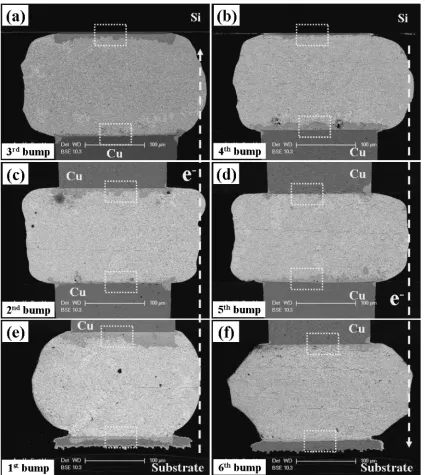
Figure 5 shows SEM images of the Sn-37Pb solder bumps after current stressing for 11 h. Figures 5(a), (c) and (e) show the left line solder bumps and Figs. 5(b), (d) and (f) the right line solder bumps shown in Fig. 2. As indicated by the arrows and the ‘‘e ’’ symbol, the electrons move from the left line bottom substrate to the top Si chip, but from the right line top Si chip to the bottom substrate. In Fig. 5, the Pb-rich phases were significantly coarsened after current stressing, com-Fig. 3 SEM micrographs of the 3-D stacked flip-chip solder joint before current stressing: (a) and (b) 1st solder bump, (c) 2nd solder
[image:3.595.90.508.73.381.2]pared with the images shown in Fig. 3. This coarsening of the phases was mainly due to the electron flow and high temperature storage of the solder bumps during the current stressing at 393 K.
For a more detailed analysis of the microstructural variation of the solder joints, enlarged views of the rectangular regions in Fig. 5 are shown in Fig. 6 (left line solder bumps) and Fig. 7 (right line solder bumps). In Fig. 6, (a) and (d) are the 1st, (b) and (e) the 2nd, and (c) and (f) the 3rd solder bumps in Fig. 2. Since electrons passed through the joint from the lower side to the upper side, the lower and upper sides acted as the cathode and anode, respectively. The IMC layers in the 1st (Fig. 6(a)) solder bump were (Ni,Cu)3Sn4 at the upper-side interface. Although, the thickness of the Ni-P layer did not change compared with the initial state before current stressing, two IMCs, (Cu,Ni)6Sn5 and Cu6Sn5, were formed on the lower side (Fig. 6(d)). The Cu atoms in the former were diffused from the Cu pad of the substrate by the acceleration of the electron flows. The thick IMC layers in the 2nd (Fig. 6(b)) and 3rd (Fig. 6(c)) solder bumps were Ni3Sn4 at the upper (anode)-side interface. At lower-(anode)-side interface, a very thick P-rich Ni (Ni3P) layer was observed under the Ni3Sn4 IMC, and Kirkendall voids were formed in the P-rich Ni layer due to the diffusion of Ni atoms from the Ni-P layer to the IMC layer. The formation period of the Kirkendall void was much shorter than during the isothermal aging at high temper-ature18,19)due to the electron flow from the cathode to anode
during electromigration and the isothermal aging at high temperature. Figure 7 shows the 4th [(a) and (d)], 5th [(b) and (e)] and 6th [(c) and (f)] solder bumps in Fig. 2. Since electrons passed through the joint from the upper to the lower side, the upper and lower sides were cathode and anode, respectively. After 11 h of current stressing, the voids that were observed at the 4th solder bump (cathode side) in the top corner on the left side of the solder bump (Fig. 7(a)) grew and propagated along the interface from the left side to the
right side. The formation of Ni3Sn4and voids tend to initiate at the current crowded region. Concerning the dimension of the sample shown in Fig. 2, the current density in the Cu interconnection line is more than 50 times higher than that inside the solder bump. Therefore, there is a transition region where the current density changes abruptly in the solder bump. This region has a higher current density than any other region in the solder bump. The simulation of current distribution in the solder bump of the flip chip structure showed that the current density in the current crowded region is much higher than the averaged current density inside the solder bump.20)During the initial current
stressing, the void quickly propagated and became signifi-cantly larger while new voids were formed in the right region of the right-side solder bump. Following void formation, the electron flows were diverted to the left and right sides of the void, causing the void to grow in these directions. Consequently, the void propagated and its increasing size led to the formation of another current crowding region in which another void can be formed. This multiple void formation restricted the paths for electron movement and directly induced the formation of Joule heating that increased the temperature of the right-side solder bump, thereby re-melting the solder bump.21) The thick IMC layers in the 4th
(Fig. 7(d)) and 5th (Fig. 7(e)) solder bumps were Ni3Sn4 at the lower (anode)-side interface.
Figure 8 shows SEM images of the Sn-37Pb solder bumps after current stressing at2:0104A/cm2and 393 K for 18 h, after which the solder joints catastrophically failed. The ENIG UBMs in the lower side of the 1st solder bump (Fig. 8(e)) and in the upper side of the 4th (Fig. 8(b)) and 5th (Fig. 8(d)) solder bumps were completely dissolved. In addition, a thick Cu-Ni-Sn IMC was formed at the upper interface of the 1st solder bump (Fig. 8(e)). Microstructural coarsening and Pb-phase accumulation occurred at the anode side (Fig. 8(b)). The dissolved ENIG UBM and the redis-tributed solder phases were caused by re-melting of the solder Fig. 4 Magnified views of the 3-D stacked flip chip solder bumps before current stressing: (a) and (d) 1st solder bump, (b) and (e) 2nd
solder bump, and (c) and (f) 3rd solder bump.
[image:4.595.86.510.70.287.2]due to Joule heating during the prolonged electromigration. At an ambient temperature of 393 K, the additional joule heating caused by the current crowding remelted the left and right line solder bumps, leading to dissolution of the ENIG UBMs on the upper side of the 4th and 5th solder bumps, respectively. This indicated that only the high current density could have caused the significant temperature increase in this solder bump that experienced a bottleneck of moving electrons.
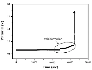
Figure 9 shows the potential versus time curves of the Sn-37Pb samples during current stressing. Before complete failure, the potential or resistance of the sample was relatively unchanged, even though the void propagation had covered a large area of the contact window, due to the small dimension of the Cu line compared with that of the solder
joint. Therefore, all the resistance was taken up by the line. As the void propagated from left to right in the 4th and 5th solder bumps, the entrance of the current into the solder bump was displaced to the front of the void. As long as the current was able to enter the solder joint, the void had very little effect overall on the resistance change, i.e., the void formation slightly increased the potential of the sample, as shown in Fig. 9. However, when the void extended across the entire contact area and consequently the solder was re-melted, the potential or resistance jumped abruptly, indicat-ing the failure of the joint. A similar result was reported in a previous study.22) Therefore, this problem of electromigra-tion strongly influences the reliability of the flip chip package, due to the abrupt, electromigration-induced elec-trical failure of the flip chip solder joint.
[image:5.595.87.512.70.545.2]4. Conclusion
In-situobservation of the 3-D flip chip solder joints during the current stressing test revealed that the electromigration of the solder’s microstructure is one of the most important factors in the failure of the 3-D flip chip packages. Therefore, this electromigration must be considered as the most critical of all the reliability factors. The failure initiation and growth in the solder joints were most highly affected by the direction of the electron movement.
A Ni3Sn4IMC layer was formed in the as-reflowed state in both the lower and upper-side interfaces. After 11 h of current stressing, the voids that were observed at the 4th solder bump (cathode side) in the top corner on the left side of the solder
bump grew and propagated along the interface from the left side to the right side.
Kirkendall voids were formed in the P-rich layer after a shortened period of reliability testing, rather than during isothermal aging. Finally, open and catastrophic failure was induced by re-melting of solder after 18 h current stressing.
Acknowledgement
The present work was carried out with the support of the Next Generation New Technology Development Program (Project No. 10030049) of the Korea Ministry of Commerce, Industry and Energy (MOCIE).
Fig. 6 Magnified views of the 3-D stacked flip chip solder bumps after current stressing for 11 h: (a) and (d) 1st solder bump, (b) and (e) 2nd solder bump, and (c) and (f) 3rd solder bump.
Fig. 7 Magnified views of the 3-D stacked flip chip solder bumps after current stressing for 11 h: (a) and (d) 4th solder bump, (b) and (e) 5th solder bump, and (c) and (f) 6th solder bump.
[image:6.595.86.514.71.290.2] [image:6.595.85.513.349.565.2]REFERENCES
1) E. C. C. Yeh, W. J. Choi, K. N. Tu, P. Elenius and H. Balkan: Appl. Phys. Lett.80(2002) 580–582.
2) A. Kumar, M. He, Z. Chen and P. S. Teo: Thin Solid Films462–463 (2004) 413–418.
3) P. Benkart, A. Heittmann, H. Huebner, U. Ramacher, A. Kaiser, A. Munding, M. Bschorr, H. J. Pfleiderer and E. Kohn: IEEE Des. Test22 (2005) 512–518.
4) J. Y. Choi, S. S. Lee and Y. C. Joo: Jpn. J. Appl. Phys.41(2002) 7487– 7490.
5) C. M. Chen and S. W. Chen: Acta Mater.50(2002) 2461–2469. 6) S. W. Chen, S. K. Lin and J. M. Jao: Mater. Trans.45(2004) 661–665. 7) T. L. Shao, Y. H. Chen, S. H. Chiu and C. Chen: J. Appl. Phys.96
(2004) 4518–4524.
8) Y. H. Lin, Y. C. Hu, C. M. Tsai, C. R. Kao and K. N. Tu: Acta Mater.53 (2005) 2029–2035.
9) H. Ye, C. Basaran and D. Hopkins: Appl. Phys. Lett.80(2003) 1045– 1047.
Fig. 8 SEM micrographs of the 3-D stacked flip chip solder bumps after current stressing for 18 h: (a), (c), (e) left and (b), (d), (f) right line solder bumps.
[image:7.595.87.507.71.543.2] [image:7.595.75.263.616.759.2]10) J. W. Nah, J. H. Kim, H. M. Lee and K. W. Paik: Acta Mater.52(2004) 129–136.
11) H. Gan and K. N. Tu: J. Appl. Phys.97(2005) 063514. 12) K. N. Tu: J. Appl. Phys.94(2003) 5451–5473.
13) T. Y. Lee, K. N. Tu and D. R. Frear: J. Appl. Phys.90(2001) 4502– 4508.
14) Y. H. Liu and K. L. Lin: J. Mater. Res.20(2005) 2184–2193. 15) J. W. Nah, K. W. Paik, J. O. Suh and K. N. Tu: J. Appl. Phys.94(2003)
7560–7566.
16) T. Y. Lee, K. N. Tu, S. M. Kuo and D. R. Frear: J. Appl. Phys.89 (2001) 3189–3194.
17) F. Laermer and A. Urban: Microelectron. Eng.67–68(2003) 349–355. 18) M. He, Z. Chen and G. Qi: Acta Mater.52(2004) 2047–2056. 19) M. He, A. Kumara, P. T. Yeo, G. J. Qi and Z. Chen: Thin Solid Films
462–463(2004) 387–394.
20) E. C. C. Yeh, W. J. Choi and K. N. Tu: Appl. Phys. Lett.80(2002) 580– 582.
21) D. G. Kim, W. C. Moon and S. B. Jung: Microelectron. Eng.83(2006) 2391–2395.
22) W. J. Choi, E. C. C. Yeh and K. N. Tu: J. Appl. Phys.94(2003) 5665– 5671.