Development of Thermoelectric Materials Consisting Solely
of Environmental Friendly Elements
Tsunehiro Takeuchi
1,2,3, Akio Yamamoto
1and Swapnil Ghodke
4 1Toyota Technological Institute, Nagoya 468–8511, Japan2PRESTO-JST, Tokyo 102–0076, Japan
3Green Mobility Collaborative Research Center, Nagoya University, Nagoya 464–8603, Japan 4Department of Crystalline Materials Science, Nagoya University, Nagoya 464–8603, Japan
A guiding principle for developing practical thermoelectric materials was constructed on the basis of simulations of thermoelectric prop-erties using linear response theory. Al-Mn-Si C54-phase, Al-Mn-Si C40-phase and higher manganese silicide (HMS), all of which consist solely of cheap, environmentally friendly elements, were selected using the guiding principle. The validity of the strategy to develop practical thermoelectric material was clearly proved by our newly prepared HMS possessing a dimensionless figure of merit exceeding unity.
[doi:10.2320/matertrans.MF201610]
(Received January 6, 2016; Accepted February 25, 2016; Published April 15, 2016)
Keywords: thermoelectrics, electronic structure, electron transport properties, thermal transport properties
1. Introduction
Recently, thermoelectric generators have attracted consid-erable interest because of their ability in recovering energy from waste heat. Development of high-performance thermo-electric materials consisting solely of environment-friendly cheap-elements would lead us to the sustainable society in which all energy sources are effectively used.
Practical thermoelectric materials had been generally de-veloped using degenerate semiconductors1) because the
elec-tronic structure of degenerate semiconductor is suitable for large magnitude of Seebeck coefficient and metallic electrical conduction, both of which together with low thermal conduc-tivity are the necessities of high-performance thermoelectric materials. It would be natural to consider that the highly so-phisticated theories of semiconductor developed for LSI, LED, Laser, solar cell, etc. could be applicable for the ther-moelectric semiconductors. Indeed, the electron transport properties of thermoelectric materials were analyzed using the semiconductor-theory2) in which carrier concentration,
carrier mobility, and effective mass were employed as con-trolling parameters.
We should stress here, however, that the use of semicon-ductor-theory is often inappropriate for explaining the elec-tron transport properties of thermoelectric materials, because the semiconductor-theory generally assumes the parabolic shape of energy-momentum (ε − k) dispersion whereas the ε − k dispersion of thermoelectric materials is not well de-scribed with the parabolic shape near the chemical potential. Indeed, temperature dependence of Seebeck coefficient ob-served for practical thermoelectric materials cannot be often accounted for by the semiconductor-theory. This fact definite-ly indicates that the persistent use of carrier concentration, carrier mobility, and effective mass for analyzing electron transport properties would not lead us to the development of highly sophisticated thermoelectric materials.
The problem about the complicated electronic structure of thermoelectric materials is easily overcomed by knowing the detailed information about the electronic structure near the
chemical potential. The first principles calculations and the highly developed experimental techniques, such as high-res-olution photoemission spectroscopy, could greatly help us to obtain the reliable information about the electronic structure. In this paper, therefore, a guiding principle for developing high performance thermoelectric materials is proposed in terms of electronic structure, and its validity is demonstrated by showing the successfully developed high-performance thermoelectric materials.
2. Guiding Principle for Developing High-Performance Thermoelectric Materials
The electron transport properties of solids are usually cal-culated in the context of linear response theory, and electrical conductivity σ(T), Seebeck coefficient S(T), and electron thermal conductivity κel(T) are expressed as eqs. (1)–(3).3–5)
σ(T )= σ(ε,T) −∂fFD(ε,T)
∂ε dε (1)
S(T )=− 1 |e|T
σ(ε,T)(ε−µ) −∂fFD(ε,T)
∂ε dε
σ(ε,T) −∂fFD(ε,T)
∂ε dε
(2)
κel(T )=e21T σ(ε,T)(ε−µ)2 −∂
fFD(ε,T)
∂ε dε
−e21T
σ(ε,T)(ε−µ) −∂fFD(ε,T)
∂ε dε
2
σ(ε,T) −∂fFD(ε,T)
∂ε dε
(3)
Here σ(ε,T), e, fFD(ε,T), and μ represent spectral
conductivi-ty, unit charge of electron, Fermi-Dirac distribution function, and chemical potential, respectively.
The performance of thermoelectric materials is generally measured by the dimensionless figure of merit ZT (= S 2σT/κ).1) By knowing that the thermal conductivity is sum
Materials Transactions, Vol. 57, No. 7 (2016) pp. 1029 to 1034
Special Issue on Recent Progress in Thermoelectrics -New Analyses and New Materials- (Thermoelectric Conversion Materials IX)
of electronic contribution and lattice contribution as κ = κel +
κlat, we transformed the equation of ZT into a slightly
modi-fied form,
ZT = S 2σT
κel
1
1+κlat/κel , (4) Two factors can be extracted from eq. (4). The first factor, A = S 2σT/κ
el, is unambiguously calculated using eqs. (1)–(3)
provided that spectral conductivity and chemical potential are obtained. Notably, the magnitude of A is less sensitive to the scattering phenomena because relaxation time τ, which gen-erally possesses a very weak energy dependence in the nar-row energy range of few kBT near the chemical potential, so τ
comes out from the integrands and vanishes in the calculation of A.6) It is also very important to note that the magnitude of
second factor B = 1/(1 + κlat/κel) always stays below unity and
increases with decreasing (κlat/κel). These facts indicate that
the magnitude of A represents the largest value of ZT obtain-able for the given electronic structure. It is explained, in other words, that for developing materials possessing a desired val-ue of ZT = a, we should employ the materials possessing a value of A much larger than a.
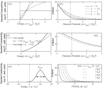
We calculated the magnitude of A as a function of chemical potential using several different models of degenerate semi-conductor possessing an energy gap near the chemical poten-tial. As a consequence of calculations shown in Fig. 1, we found that the magnitude of A becomes extremely large when the chemical potential is located in the energy gap. This seemingly unusual situation is realized even for degenerate
semiconductors at high temperatures provided that the Fermi energy is located between band edge and a large peak existing in the electronic density of states near the band edge. In order to confirm this fact, the temperature dependence of chemical potential was calculated for two different models: single band model and two-band model consisting of wide and narrow bands. The Fermi energy was located so as to become the same carrier concentration in the both models.
If we assume that the spectral-conductivity is described as σ(ε, T) = C(ε − εedge)n, the factor A at a given chemical
poten-tial possesses a larger value with the larger value of exponent n. The magnitude of constant parameter C, on the other hand, does not contribute to the variation of A, but affects the mag-nitude of B; a large magmag-nitude of C leads to an increase of B through the reduction of (κlat/κel). It would be also very
im-portant to note that the magnitude of B is further increased if the lattice thermal conductivity is greatly decreased by the complex structure7), rattling mode8), and/or anharmonic
os-cillation of lattice vibration.9)
On the basis of facts described above, we propose the ne-cessities of electronic structure for high-performance thermo-electric materials possessing a large magnitude of A; (a) large band gap exceeding 10 kBTA where TA indicates the
tempera-ture of practical applications, (b) a large peak in electronic density of states staying at a few kBTA apart from the edge of
energy gap, and (c) multiple band existing near the band edge in the energy range where the electrons contribute the electri-cal properties. The condition (a) prohibits the reduction of Seebeck coefficient in association with bi-polar diffusion ef-Fig. 1 (a) Model of spectral conductivity and (b) A = S 2σT/κ
el calculated using eqs. (1)–(3). The model 1 consists of one band, and the spectral conductivity
is represented by σ(ε, T) = C(ε − εedge)n. At a given chemical potential, A becomes larger with large number of n, and A is getting larger when the chemical
potential is located in the band gap. The model 2 consists of 2 bands with n = 3/2. One of the bands is located 1kBT above the others. The magnitude of A
[image:2.595.127.470.69.360.2]fect, and the condition (b) allows the chemical potential to move drastically with increasing temperature. The condition (c) is important for the large magnitude of Seebeck coeffi-cient. The materials possessing these characteristics in their electronic structure must exhibit a large magnitude of A with an appropriate Fermi energy.
If the materials possessing the conditions (a)–(c) are fur-ther characterized by (e) the complex structure7), (f) rattling
mode8), and/or (g) anharmonic oscillation of lattice
vibra-tion9), the magnitude of ZT should be greatly increased
through a large magnitude of B = 1/(1 + κlat/κel).
Neverthe-less, it would be very difficult to find such an ideal material possessing all the required conditions.
We should mentioned here that even without using the con-ditions (e)–(g) the magnitude of B could be effectively in-creased using the partial substitution of elements that have a large difference in atomic mass from that of constituent ele-ments. We are not seriously concerned about the effect of dis-ordering on the electron mean free path. In many thermoelec-tric materials, the conduction electrons stay near the strong scattering limit10,11) due to the small Fermi surface and the
chemical disordering introduced for carrier doping, because the long Fermi wavelength makes the conduction electrons near the Fermi level easily lose the coherence even under the small amount of impurity elements. In such a condition, the mean free path of electrons cannot be further shortened with the additionally introduced disordering, meanwhile the pho-non mean free path, that is generally kept long in the degen-erate semiconductors, should be greatly reduced by the par-tial substitution of elements possessing significantly different atomic mass.12–14) Therefore, if impurity states are not
pro-duced near the chemical potential at the element substitution, the lattice thermal conductivity will be greatly reduced with-out seriously affecting the electron transport properties.
3. Al-Mn-Si C54-Phase (Si2Ti Structure) and C40-Phase
(CrSi2 Structure)
According to the guiding principle described above, we se-lected two intermetallic compounds, Al-Mn-Si C54-phase (Si2Ti structure, oF24) and Al-Mn-Si C40-phase (CrSi2
struc-ture, hP9) stabilized at around Al32Mn34Si3415) and
Al27.5Mn33.0Si39.516), respectively. Both materials are
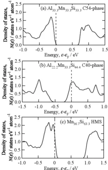
charac-terized by the two-dimensional honeycomb lattice consisting of Al and Si with Mn at the center of hexagon, and the two-di-mensional planes are stacked with four different positions in C54-phase and three positions in C40-phase. The similarity in local atomic arrangements naturally leads to the similarity in electronic density of states as shown in Fig. 2. It is clearly confirmed that these selected materials possess the character-istics of electronic structure (a)–(c), which are the necessities of high-performance thermoelectric materials.
We found that these intermetallic compounds character-ized by non-toxic, abundant constituent emelents indeed pos-sess a large magnitude of Seebeck coefficient |S| > 200 μVK−1,
metallic electrical conduction with a relatively low values of electrical resistivity ρ < 10 mΩcm, and consequently large magnitude of A exceeding 2.15–17) The magnitude of power
factor PF = S 2σ reaches 2.1 mWm−1K−2 at 500 K for n-type
Al33.0Mn34.0Cr1.0Si30.0 C54-phase and 1.1 at 440 K for n-type
Al27.5Mn31.0Cr2.0Si39.5 C40-phase. The large magnitude of
power factor observed for the both compounds indicates that the conditions (a)–(c) of electronic structure are usable for easily finding materials possessing electron transport proper-ties suitable for practical thermoelectric material.
Despite the electron transport properties suitable for ther-moelectric materials, the large lattice thermal conductivity, 10 Wm−1K−1 of C54-phase17) and 4.2 Wm−1K−1 of
C40-phase16) prevented us from obtaining a large magnitude of
dimensionless figure of merit ZT. The magnitude of ZT was, hence, limited to less than 0.15. Note here that the difference of lattice thermal conductivity between C54-phase and C40-phase would be related to the number of atoms in the unit structure, N = 6 of C54-phase and 9 of C40-phase, because larger number of N naturally leads to enhanced umklapp pro-cess of phonon scatterings, reduced mean group velocity of phonons, and consequently to small magnitude of lattice ther-mal conductivity.7)
For effectively reducing lattice thermal conductivity of these compounds, we employed small amount of element substitutions using the heavy elements that do not produce any impurity states near the chemical potential at the substi-tution. The cluster calculations suggested us that (Re + Ru) and W produce no impurity states near the chemical potential when these elements were substituted for Mn in C54-phase and C40-phase, respectively.16,17) The experimentally
ob-served thermoelectric properties are shown in Fig. 3. The lat-tice thermal conductivity was reduced into 2.9 Wm−1K−1 for
C54-phase and 1.9 Wm−1K−1 for C40-phase when small
Fig. 2 Electronic density of states of (a) Al-Mn-Si C54-phase, (b) Al-Mn-Si C40-phase, and (c) HMS. A relatively wide band gap is formed in all the compounds. The peaks near the band edge indicate that these materials possess large magnitude of Seebeck coefficient, and rather complicated energy dependence means that the multiple bands near the band edges. The calculations were performed with FLAPW-GGA method.
[image:3.595.338.513.70.346.2]amount of heavy elements were introduced in the samples. In sharp contrast to the large reduction in lattice thermal con-ductivity, the electron transport properties were essentially kept unchanged. The consequently obtained ZT was plotted as a function of temperature in Fig. 4. The maximum value of ZT was increased up to 0.38 (n-type) at 540 K and 0.24 (n-type) at 440 K for Al37.0Mn26.0Ru3.0Re3.0Fe1.0Si30.0
C54-phase17) and Al
27.5Mn29.0W3.0Fe1.0Si39.5 C40-phase16),
respec-tively.
Although we succeeded in increasing ZT for both C54-phase and C40-C54-phase, the resulting values of ZT were still smaller than unity mainly because the energy gap was smaller than that estimated from the first principles calculations. The difference in width of energy gap between the experiments and calculations was confirmed by comparing the tempera-ture dependence of Seebeck coefficient. Figure 5 shows the temperature dependence of Seebeck coefficient obtained by both experiments and calculations. The experimentally ob-tained magnitude of Seebeck coefficient |S| showed good
agreement with the calculated ones at low temperatures, but became definitely smaller at high temperature regardless of the carrier concentrations. The reduction of |S| at high tem-Fig. 4 Dimensionless figure of merit observed for
Al37.0Mn26.0Ru3.0Re3.0Fe1.0Si30.0 C54-phase17) and
Al27.5Mn29.0W3.0Fe1.0Si39.5 C40-phase.16)
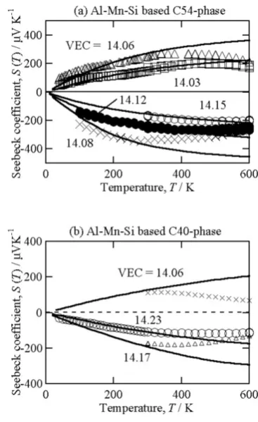
Fig. 5 Measured (markers) and calculated (solid lines) Seebeck coefficient of Al-Mn-Si based (a) C54-phase and (b) C40-phase. At low tempera-tures, the measured data showed very good consistency with the calculat-ed one, but its magnitude becomes smaller at high temperature because of the bipolar diffusion effects. This fact definitely indicates that the calcu-lated energy gap is overestimated presumably due to the hypothetical or-dering between Al and Si used for the calculations.
Fig. 3 (a) Seebeck coefficient. (b) electrical resistivity, and (c) thermal conductivity of Al-Mn-Si based C54-phase.17) Those for Al-Mn-Si C40-phase were
plotted in (d)–(f).16) With increasing concentration of heavy elements, the lattice thermal conductivity were greatly reduced while the electron transport
[image:4.595.127.467.72.288.2] [image:4.595.332.516.354.654.2] [image:4.595.47.290.357.532.2]peratures is caused by the bi-polar diffusion effect in associa-tion with the excitaassocia-tion of electrons from valence band to conduction band. The lower temperature of bi-polar diffusion effect definitely indicates that the energy gap of both com-pounds is smaller than that expected from the first principles band calculations. The unusual overestimation of energy gap in band calculations was presumably brought about by the inappropriate use of structure ordering between Al and Si, though the Al and Si are essentially coexist together in the same atomic sites in both compounds.
4. Higher Manganese Silicide
Higher manganese silicide (HMS) obtainable at around Mn36.4Si63.6 (MnSi1.75) and Al-Mn-Si C54-phase are
classi-fied into the group of Nowotny chimney ladder phases18) and
consequently possess a good similarity in local atomic ar-rangements. The similar local atomic arrangements naturally lead to similarity in electronic structure as shown in Fig. 2., and hence similar electron transport properties. It would be very important to note that the temperature dependence of electron transport properties of HMS19) indicates presence of
a large energy gap of ~0.8 eV in width, which is comparable with that predicted by the band calculation. The consistency of energy gap between experiment and calculation would be closely related to the absence of chemical disordering be-tween Al and Si in HMS.
The p-type HMS is known to possess a large value of ZT ~ 0.46 at around Mn36.4Si63.619) with its lattice thermal
conduc-tivity of κlat ~ 2 Wm−1K−1.19,20) This fact strongly let us
be-lieve that the value of ZT can be further increased provided that a small amount of 5d transition metal elements is substi-tuted for Mn in the same manner as we performed for the Al-Mn-Si C54-phase and C40-phase.
We employed Re as the element of partial substitution for Mn, partly because Re stays in the same column in the peri-odic table to presumably produce no serious impurity states
in the energy gap, and partly because Re-substitution for Mn led the effective reduction of κlat without a serious variation in
electron transport properties of Al-Mn-Si C54-phase.17) By
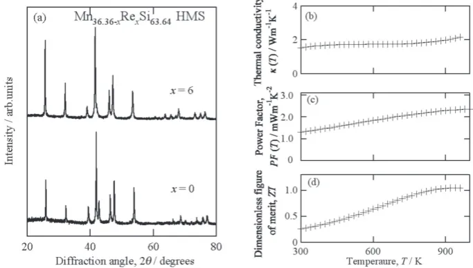
introducing 6 at.% Re in HMS, we succeeded in obtaining 60% reduction of κlat from that of Re-free sample.21) Figure 6
(a) shows the powder XRD patterns of samples obtained at Mn36.4Si63.6 and Mn30.4Re6.0Si63.6, and their thermal
conduc-tivity and power factor are shown in Fig. 6 (b) and (c), respec-tively. The maximum magnitude of ZT of Mn30.4Re6.0Si63.6
shown in Fig. 6 (d) was increased up to 1.04 at around 920 K from 0.46 of Mn36.4Si63.6. The consequently obtained, large
value of ZT for the HMS lends a great support to the validity of our newly constructed guiding principle for practical ther-moelectric materials.
5. Discussions
In this section, the method to find the materials possessing (g) anharmonic oscillation of lattice vibration in crystal struc-ture is discussed. The condition of (g) is realized when the atomic potential about some specific atomic sites in the lattice is rather shallow than that in usual materials. This character-istic in atomic potential sometime leads to ionic conduction, which is often observed in oxides and chalcogenides where some of the constituent elements are strongly connected by covalent bonding and some of atoms are connected by ionic bonds. If the ions in chalcogenides possess full filled d-bands near the Fermi energy, such as those in Cu and Ag, the atomic potential about the ions would become much shallower and the ions possess anharmonic oscillation even at low tempera-ture. If these materials of ionic conduction possess the condi-tion (a)–(c) in their electronic structure, we would have a large magnitude of both A and B and hence a large magnitude of ZT.
Indeed, bulk materials possessing an extremely large mag-nitude of ZT > 1 were found recently in chalcogenides such as Cu2Se22) and CuGaTe223). These materials are definitely
char-Fig. 6 (a) Powder XRD patterns of Mn36.4Si63.6 and Mn30.4Re6.0Si63.6 HMS s. No impurity phase was found in the samples. (b) Thermal conductivity, (c)
power factor, and (d) dimensionless figure of merit of Mn30.4Re6.0Si63.6 HMS are plotted in (b)–(d), respectively. By using 6 at.% Re substitution for Mn in
Mn36.4Si63.6 HMS, we succeed in obtaining sample possessing ZT = 1.04 at around 900 K. The infromation anbout sample preparation techniques and
composition dependence of thermoelectric properties will be reported elsewhere.21)
[image:5.595.125.467.75.269.2]acterized by the very small magnitude of lattice thermal con-ductivity together with the large magnitude of power factor presumably due to the anharmonic lattice vibration. This fact indicates that both electronic structure and lattice vibrations of these compounds are best suited for the thermoelectric ma-terials.
In the materials consisting both of metals and metalloids such as Cu2Se and CuGaTe2, several different chemical bonds
exist to make the atomic potential anharmonic. This consider-ation was confirmed in our recent work on In2S3 possessing
very small lattice thermal conductivity less than 1 W m−1K−1.24) We selected this compound because it
con-sists of metal (Indium) and metalloid (sulfur) and possesses the appropriate electronic structure for thermoelectricity. Consequently, it possessed relatively large dimensionless fig-ure of merit exceeding 0.4.
We stress here that we could find other high-performance thermoelectric materials in chalcogenides if we carefully in-vestigated their electronic structure using first principles cal-culations. Nevertheless, it would be mentioned before pass-ing that even if the magnitude of ZT is very large, materials with ionic conduction cannot be uses as practical thermoelec-tric materials because inhomogeneous distribution of ion caused by the electrical current would lead to serious effect on the phase stability and/or electron transport properties. We should, therefore, find the chalcogenides possessing atoms nearly conducting but staying in the specific sites in the unit cell.
6. Conclusion
In this paper, we proposed the conditions of electronic structure to developing practical thermoelectric materials to-gether with the method for effectively reducing lattice ther-mal conductivity without seriously affecting electron trans-port properties. By using the proposed strategy, we succeeded in obtaining materials possessing a large magnitude of di-mensionless figure of merit ZT > 1.0 in the alloy systems con-sisting solely of environmental-friendly elements, Mn, Si, and Re. This fact definitely indicated that our newly con-structed guiding principle works for finding new thermoelec-tric materials of high performance.
Acknowledgements
This research was supported by the JST PRESTO
pro-gram (New Materials Science and Element Strategy) and sup-ported by JSPS KAKENHI Grant Number 26630332 and 26289236.
REFERENCES
1) A. F. Ioffe: Semiconductor Thermoelements and Thermoelectric
cool-ing, Infosearch limited, London, (1957).
2) G. Berns: Solid State Physics, Academic Press, Inc., Orland, FL, (1985).
3) N. F. Mott: The Theory of the Properties of Metals and Alloys, Dover Publications, Inc. New York, NY (1958).
4) J.M. Ziman: Principles of the Theory of Solids, Cambridge University Press, New York, NY (1972).
5) J. S. Dugdale: The Electrical Properties of Metals and Alloys, Edward Arnold, London, (1977).
6) T. Takeuchi: New Thermoelectric Materials with Precisely Determined
Electronic Structure and Phonon Dispersion in Thermoelectrics and its Energy Harvesting, Ed. by D. Rowe, CRC press, Boca Raton, FL (2012).
7) T. Takeuchi, N. Nagasako, R. Asahi and U. Mizutani: Phys. Rev. B 74 (2006) 054206.
8) B.C. Sales, D. Mandrus, B.C. Chakoumakos, V. Keppens and J.R. Thompson: Phys. Rev. B 56 (1997) 15081.
9) Y. Wang, B. Qiu, A.J.H. McGaughey, X. Ruan and X. Xu: J. Heat Transfer 135 (2013) 091102.
10) A.F. Ioffe and A.R. Regel: Prog. Semicond. 4 (1960) 237.
11) N.E. Hussey, K. Takenaka and H. Takagi: Philos. Mag. 84 (2004) 2847.
12) P.G. Klemens: Proc. Phys. Soc. Lond. A 68 (1955) 1113.
13) Y. Nishino, S. Deguchi and U. Mizutani: Phys. Rev. B 74 (2006) 115115.
14) T. Takeuchi, Y. Terazawa, Y. Furuta, A. Yamamoto and M. Mikami: J. Elec. Mater. 42 (2013) 2084.
15) T. Takeuchi, Y. Toyama, A. Yamamoto, H. Hazama and R. Asahi: Mater. Trans. 51 (2010) 1127.
16) A. Yamamoto, M. Miyazaki, M. Inukai, Y. Nishino and T. Takeuchi:
Jpn. J. Appl. Phys. 54 (2015) 071801.
17) A. Yamamoto, H. Miyazaki and T. Takeuchi: J. Appl. Phys. 115 (2014) 023708.
18) D.C. Fredrickson, S. Lee, R. Hoffmann and J. Lin: Inorg. Chem. 43 (2004) 6154.
19) Y. Miyazaki, Y. Saito, K. Hayashi, K. Yubuta and T. Kajitani: Jpn. J. Appl. Phys. 50 (2011) 035804.
20) V. Ponnambala, D.T. Morelli, S. Bhattacharya and T.M. Tritt: J. Alloy. Compd. 580 (2013) 598.
21) A. Yamamoto, S. Ghodke, H. Miyazaki, M. Inukai, Y. Nishino and T. Takeuchi: Jpn. J. Appl. Phys. 55 (2016) 020301.
22) X. Su, F. Fu, Y.-G. Yan, G. Zheng, T. Liang, Q. Zhang, X. Cheng, D.-W. Yang, H. Chi, X.-F. Tang, Q. Zhang and C. Uher: Nature Communica-tions 5 (2014) 4908.
23) T. Plirdpring, K. Kurosaki, A. Kosuga, T. Day, S. Firdosy, V. Ravi, G.J. Snyder, A. Harnwunggmoung, T. Sugahara, Y. Ohishi, H. Muta and S. Yamanaka: Adv. Mater. 24 (2012) 3622.