Zixue Su
A Thesis Submitted for the Degree of PhD at the
University of St Andrews
2010
Full metadata for this item is available in Research@StAndrews:FullText
at:
http://research-repository.st-andrews.ac.uk/
Please use this identifier to cite or link to this item: http://hdl.handle.net/10023/1019
This item is protected by original copyright
Zixue Su
PhD Dissertation
School of Chemistry, University of St. Andrews
Supervisor: Dr. Wuzong Zhou
Declaration
I, ………., hereby certify that this thesis, which is
approximately ………. words in length, has been written by me, that it is the record
of work carried out by me and that it has not been submitted in any previous application for a
higher degree.
date ………. signature of candidate ……….
I was admitted as a research student in ………. [month, year] and as a candidate for
the degree of ………. in ………. [month, year]; the higher study for
which this is a record was carried out in the University of St Andrews between ………[year]
and ………[year].
date ………. signature of candidate ……….
I hereby certify that the candidate has fulfilled the conditions of the Resolution and Regulations
appropriate for the degree of ……… in the University of St Andrews and that
the candidate is qualified to submit this thesis in application for that degree.
date ………. signature of supervisor ……….
In submitting this thesis to the University of St Andrews we understand that we are giving
permission for it to be made available for use in accordance with the regulations of the
University Library for the time being in force, subject to any copyright vested in the work not
being affected thereby. We also understand that the title and the abstract will be published, and
that a copy of the work may be made and supplied to any bona fide library or research worker,
that my thesis will be electronically accessible for personal or research use unless exempt by
award of an embargo as requested below, and that the library has the right to migrate my thesis
into new electronic forms as required to ensure continued access to the thesis. We have obtained
any third-party copyright permissions that may be required in order to allow such access and
Access to all of printed copy but embargo of all of electronic copy for a period
of ……2…… years (maximum five) on the following ground:
publication would be commercially damaging to the researcher, or to the supervisor, or the
University;
publication would preclude future publication;
publication would be in breach of law or ethics
Acknowledgements
Firstly I am cordially grateful to my supervisor Dr Wuzong Zhou for his help of imparting the
knowledge of electron microscopy, crystallography, and directing me to design the experiments,
solving problems in experiments and writing scientific papers and dissertation. Moreover he took
care of my life in St Andrews and taught me to become a true researcher. He is one of the
persons I respect and appreciate mostly in my life.
And I would like to thanks Prof. M. Bühl from the school of chemistry in the University of St
Andrews for the theoretical computation in the field enhanced dissociation of water; Mr Shijing
Lu from department of physics of Zhejiang University in China for the theoretical simulation in
the ionic convection during metal anodisation.
Subsequently, .I would also like to thank Mr. Ross Blackley, who trained me on high
resolution transmission electron microscopy and x-ray diffraction; Prof. Ifor Samuel of Physics
Department for accessing the field emission gun SEM, Mrs Sylvia Williamson for her help of IR
experiments, Miss Julie Nairn for the help of gold deposition and surface polishing.
I need to say “thank you” to Mr. Wenbo Yue who gave me many helps in discussions of my
experiments and operations of HRTEM and XRD, to Xiaoxiang Xu who help me in the IR
characterization, and to other guys in the University of St Andrews who have been so nice to me.
I should thank my parents who brought me up and always supported me. They are invaluable
to me in the world.
Abstract
An equifield strength model has been established to elucidate the formation mechanism for
the highly ordered alumina pore arrays and titanium oxide nanotubular arrays prepared via a
common electrochemical methodology, anodisation. The fundamentals of the equifield strength
model was the equilibrium between the electric field driven oxidation rate of the metal and
electric field enhanced dissolution rate of oxide. During the anodic oxidation of metal, pore
initiation was believed to generate based on dissolution rate difference caused by inhomogeneity
near the metal/oxide interface. The ionic nanoconvection driven by the electric force exerted on
the space charge layer in the vicinity of electrolyte/oxide interface is established to be the main
driving force of the pore ordering at the early stage of the anodisation. While the equifield
strength requirement governs the following formation of the single pore and the self-ordering of
random distributed pore arrays during the anodisation process.
Hexagonal patterned Al2O3 nanopore arrays and TiO2 nanotubular arrays have been
achieved by anodisation of corresponding metal substrates in proper electrolytes. The two
characteristic microstructural features of anodic aluminium oxide (AAO) and anodic titanium
oxide (ATO) were investigated using scanning electron microscopy (SEM) and high resolution
transmission electron microscopy (HRTEM). The observations of the hemispherical
electrolyte/oxide and oxide/metal interfaces, uniform thickness of the oxide layer, as well as
self-adjustment of the pore size and pore ordering can be well explained by the equifield strength
model.
Field enhanced dissociation of water is extremely important in determination of the porosity
of anodic metal oxide. The porosity of AAO and ATO films was found to be governed by the
relative dissociation rate of water which is dependent on anodisation conditions, such as
electrolyte, applied voltage, current density and electric field strength. Using an empirical
method, the relations between the porosity of the AAO (ATO) films and the anodisation
parameters, such as electric field strength, current density and applied voltage, have been
established. Besides, the extent that an external electric field can facilitate the heterolytic
dissociation of water molecule has been estimated using quantum-chemical model computations
oxide films can be understood and controlled more precisely.
Additionally, the impacts of other factors such as the electrolyte type and the temperature
effect on the morphology of the anodic products were also investigated. Some important
experimental evidences on the pore diameters variation with applied voltage in the anodisation of
aluminium and the titanium were obtained for future investigation of the anodic metal oxide
Contents
Decl aratio n ………….……….. ... .. I
Ackn o wl ed gem en t s ………….………. III
A b s t r a c t … … … … . … … … . . . I V C o n t e n t s … … … … . … … … . . V I
1 Introduction ...1
1.1 Anodisation...2
1.2 Anodic aluminium oxide ...3
1.2.1 Barrier-type AAO films ...4
1.2.2 Porous-type AAO films ...6
1.2.3 Chemical reactions in Al anodisation ...9
1.2.4 Pore formation in porous AAO films ...10
1.2.5 Self-ordering of pores in porous AAO films ...12
1.2.6 Impact factor on the anodic film parameters ...16
1.3 Anodic titanium oxide ...17
1.3.1 Fabrication of ATO nanotubes ...18
1.3.2 Formation mechanism of ATO nanotubes ...22
1.4 Other anodic metal oxides ...26
1.4.1 Anodisation of hafnium ...26
1.4.2 Anodisation of niobium ...27
1.4.3 Anodisation of tantalum ...28
1.4.4 Anodisation of tungsten ...28
1.4.5 Anodisation of vanadium...29
1.4.6 Anodisation of zirconium ...29
1.5 Applications of porous AAO and ATO ...30
1.5.1 Application of porous anodic aluminium oxide ...30
1.5.2 Application of porous anodic titanium oxide ...35
1.6 Aims and Objectives ...43
2 Experiments ...44
2.1 Anodisation method...44
2.1.1 Anodic aluminium oxide ...45
2.1.2 Anodic TiO2nanotubes...45
2.2 Characterization methods ...46
2.2.1 Electron microscopy ...46
2.2.2 X-ray diffraction ...59
2.2.3 Infrared spectroscopy ...63
2.2.4 Computational chemistry...63
3 Formation of Self-ordered AAO Nanopore Arrays ...66
3.1 Equifield strength model and its application in the AAO formation...67
3.1.2 Equifield strength model ...70
3.1.3 Pore initiation ...71
3.1.4 Growth of single pore ...73
3.1.5 Self-adjustment of pores...73
3.1.6 Impact factor on the ordering of AAO pore arrays...77
3.2 Porosity of AAO ...78
3.2.1 Relative dissociation of water and the porosity of AAO ...78
3.2.2 Ratio of dissolved Al cations from the two interfaces...82
3.2.3 Relations between the porosity and anodisation conditions...84
3.3 Pore size variation with voltage of AAO films...89
3.4 Local temperature effect on the dissolution rate...94
3.5 The nm/v ratio for the barrier layer ...95
4 Formation of Self-ordered ATO Nanotubular Arrays ...97
4.1 Microstructures of ATO ...99
4.2 Chemical reactions ...101
4.3 Equifield strength requirement and the ATO formation mechanism ...103
4.4 Formation of O-rings ...106
4.5 Porosity of anodic titanium oxide...108
4.6 Pore size variation with voltage of ATO films ...115
4.7 Dissolved Ti4+cations from two interfaces ...119
4.8 Crystallisation of anodic titanium oxide...120
5 Field Enhanced Dissociation of Water ...123
5.1 Theoretical computation for the field present water dissociation...124
5.1.1 Details of the computation...124
5.1.2 Results of the computation ...126
5.2 The experimental fit for the theoretical computation ...130
6 Ionic Nanoconvection in the Early Stage of Anodisation...136
6.1 Details of the theoretical simulation of the ionic convection ...139
6.2 Results of the ionic convection simulation...140
7 Conclusions and Future Work ...144
7.1 Conclusion ...144
7.2 Future work ...145
References ...148
1 Introduction
The research realms of fabrication and application of nanomaterials have triggered tremendous
technological and scientific interest from various disciplines in the recent years. Compared with
the bulk materials, nanomaterials often have unique electronic and optical properties, many of
which are yet to be investigated. Nanostructured metal oxide material devices have exhibited
variety of high-tech applications such as dye-sensitized solar cells,1 displays and smart
windows,2 and biosensors,3 lithium batteries,4 and supercapacitors.5 Indeed, to fulfill the great
promise and expectation of nanomaterials, scientists and chemists have developed a number of
new synthetic techniques and patterning methods, such as self-assembly,6 mechanochemistry,7
chemistry by microwave,8 lithography9 or template- and membrane-based synthesis.10 Among
these methods, the anodising approach is able to build metal oxide nanopores of controllable
pore size, good uniformity, array-orderly, and conformability over large areas at low cost via a
simple experimental procedure.
Anodic metal oxides have diverse applications in the prevention of corrosion of metal
substrates from their service environment,11 forming capacitor dielectrics,12,13 templating
nanomaterials14-19 and in many other fields such as catalysis, optics and electronics.20-23The best
known porous anodic oxide, anodic aluminium oxide (AAO), was first reported 50 years ago24-27
and is now commercially available. It can be used as an ideal template for preparing various
nanoparticles, nanowires and nanotubes. Porous anodic oxide films have also been achieved on
surfaces of many other metals, sometimes the so-called valve metals, e.g., titanium,28-30
hafnium,31niobium,32tantalum,33tungsten,34vanadium,35and zirconium.36
The concept that the formation of porous anodic metal oxides is based on two continuous
processes, one being oxide dissolution at the electrolyte/oxide interface and the other being
oxidation of metal at the oxide/metal interface, is widely accepted by former researchers.
However, the formation mechanism of these pores, often hexagonally ordered, is much more
complicated than people normally predicted. There remain a number of questions from the pore
initiation at the very beginning to the formation of highly ordered patterned pore arrays at the
formation mechanism of nanoporous anodic metal oxides,37-42 there is still much work to do in
order to understand fully the electrochemical process during the anodisation. Then it will be
possible to optimize the anodisation conditions to manage precise control of the growth of the
anodic metal oxide, finally improving and widening their scientific and industrial applications.
1.1 Anodisation
An oxide film can be grown on certain metals – aluminium, titanium, tantalum, etc. by an
electrochemical process called anodisation. The process is called "anodisation" because the part
to be treated forms the anode electrode of the processing electrical circuit. Anodisation can be
used to increase the thickness of the natural oxide layer on the surface of metal parts, which can
increase corrosion and wear resistance, and provides better adhesion for paint primers and glues
than bare metal. Besides the conventional application in prevention of corrosion of the metal
substrate from their service environment and being the capacitor dielectrics, anodic metal oxide
films have widened their use in many other aspects in catalysis, optics, electronics, and in
nanotechnology.
Anodic films are generally much stronger and more adherent than most types of paint and
metal plating, making them less likely to crack and peel. It has been widely applied to protect
aluminium alloys, but is not a useful treatment for iron or carbon steel because these metals
exfoliate when oxidized; i.e. the iron oxide (also known as rust) flakes off, constantly exposing
the underlying metal to corrosion. Except aluminium, porous anodic oxide films have also been
achieved on surfaces of many other valve metals, such as titanium, hafnium niobium, tantalum,
tungsten, vanadium, and zirconiumet. al. The surfaces of these so-called valve metals could be
immediately covered with a native oxide film of a few nanometers when these metals are
exposed to oxygen containing surroundings. While these oxides retard the rate of reaction on the
metal surface inherently, for each of these valve metals there are some process conditions that
may promote growth of a thin, dense, barrier oxide of uniform thickness. The thickness and the
properties of such a barrier layer vary greatly among different methods.
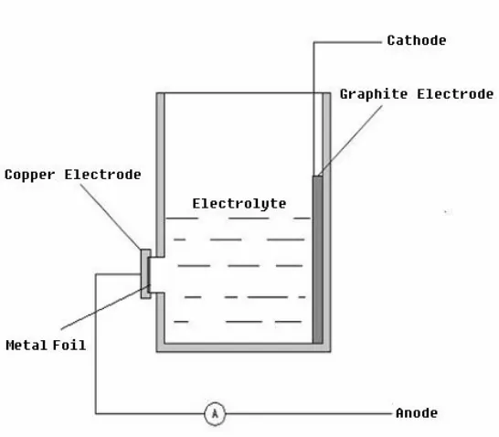
In an anodising cell, a piece of metal foil is used as anode by connecting it to the positive
The cathode can be a plate or rod of carbon, lead, nickel, stainless steel – any electronic
conductor that is unreactive (inert) in the anodising bath. When the circuit is closed, electrons are
withdrawn from the metal at the positive terminal, allowing ions at the metal surface to react
with water to form an oxide layer on the metal. The electrons return to the bath at the cathode
where they react with hydrogen ions to make hydrogen gas.
A bath electrolyte is selected in which the oxide is insoluble, or at least dissolves at a lower
rate than its deposition, and eventually an adherent oxide layer grows. The bath composition is
the primary determinant of whether the film will be a barrier or porous. Barrier oxide grows in
near neutral solutions in which the metal oxide is hardly soluble. Porous oxide grows in acidic
electrolyte in which oxide can not only be deposited but also dissolves.
1.2 Anodic aluminium oxide
The history of anodisation of aluminium dates back to the beginning of the last century.
Protection and decoration of Al and its alloys by means of an anodic treatment was developed as
early as the 1920’s.11 Anodisation processes have been applied for various metals such as
aluminium, magnesium, niobium, tantalum, titanium, tungsten, vanadium, zinc, and zirconium,
among which the anodic alumina films are most commonly applied to protect and decorate
aluminium alloys. Before anodisation, aluminium metal could react with oxygen in air, forming a
thin barrier oxide layer with a thickness of 2-3 nm next to the metal surface.43 This compact
barrier oxide layer protects the surface from further oxidization by its service environment and is
an excellent electrical insulator.
When an aluminium foil covered with a native oxide is made the anode in an typical anodising
cell, the voltage across the oxide can be increased, without initiating current flow, until the field
in the oxide is large enough to drive aluminium and oxygen ions through the oxide.44,45The ionic
transport across the oxide layer under a high field plays an important role in oxide formation
during the anodisation of aluminium.46Electric field strength in a range from 108to 109 V/m is
required to drive the ions crossing the oxide layer. Once a sufficient high external voltage is
applied, hydrogen ions are reduced to produce hydrogen gas at the cathode and aluminium is
by high field, since if it is an electronic current, then water would be oxidized to evolve oxygen,
which is not seen or at least not significant in experiments.
Depending on the electrolyte used, two types of anodic aluminium oxide layers could be
produced: barrier-type films with uniform thickness in a near neutral electrolyte and porous
anodic oxide films containing dense nanoscale pores in an acidic or alkaline electrolyte.47,48
1.2.1 Barrier-type AAO films
When Al is anodised in the electrolytes where the formed oxide film is completely insoluble
such as ammonium tartrate solution,49nonporous barrier-type films will be produced. Figure 1-1
shows a typical barrier-type AAO films grown on the top of the metal substrate.
Figure 1-1.SEM image of a cross section of an amorphous aluminium oxide layer (top) grown
on aluminium (bottom) in 0.16 M ammonium tartrate at 20 °C with a current density of 10
mA/cm2. The oxide thickness is about 220 nm at a stable voltage of 200 V, equivalent to 1.1
nm/V. (By Furneauxet al, 1978)49
It has been generally accepted that during the formation of nonporous anodic alumina in a near
neutral electrolyte, aluminium oxide simultaneously grows at both the electrolyte/oxide and
oxide/metal interfaces. Oxygen-containing anions, O2−/OH− mainly coming from dissociation of
water at the electrolyte/oxide interface move inwards to react with aluminium at the oxide/metal
interface to form oxide. At the same time, Al3+cations move outwards from the metal surface to
near neutral electrolyte, a barrier layer forms at near 100% efficiency,i.e. almost all of the Al3+
cations migrating from the oxide/metal interface would contribute to the formation of Al2O3 at
the electrolyte/oxide interface.50Brownet al. gave a ratio of oxide formation at oxide/electrolyte
and oxide/metal interfaces to be 40%:60%. Such films grow by counter migrations of Al3+ and
O2−ions, with the latter accounting for about 60% of the ionic current.51 Figure 1-2 illustrates a
cation transport number of 0.4 in the formation of a barrier type oxide layer at 100% efficiency
by Skeldonet al.52
Figure 1-2. Schematic diagrams illustrating dimensional changes of an aluminium specimen
following anodising. (a) Initial aluminium, with a thin air-formed oxide film. An immobile
marker layer, shown as a dashed line, is incorporated into the oxide film. (b) An aluminium foil
anodized at 100% efficiency, with formation of a barrier anodic film. The marker layer is located
at a depth of 40% of the film thickness, in a plane corresponding to that of the original metal
surface. (By Skeldonet al, 2006)52
It was reported that, when aluminium was anodised in a sodium borate-ethylene glycol
electrolyte, the fraction of the total charge carried by cations (tAl3+) was about 0.6,whereas in
aqueous ammonium citrate tAl3+varied from 0.37 to 0.72 as the current density increased from
0.1 to 10 mA/cm2.53 Some other values of the transport numbers of Al3+ cations were also
detected.52,54,55 The total ionic current density (j) under a high field conduction relates to the
electric field strength (E) through an exponential law j = j0exp(βE) where j0 and β are
temperature-dependent constants involving parameters of ionic transport in a particular
The final thickness of the barrier oxide is proportional with the applied voltage, and has a
small deviation with temperature and the electrolyte characteristics. A typical anodisation ratio
for aluminium anodised in a near neutral electrolyte is about 1.4 nm/V.47,56 Apart from the
temperature of the electrolyte, barrier-type film thickness is controlled mainly by the voltage
applied. The maximum film thickness attainable for barrier-type films is restricted to a voltage
below the oxide breakdown voltage value, i.e., 500-700 V, which corresponds to 7000-10,000
Å.57
1.2.2 Porous-type AAO films
When Al was anodised in acidic solution, due to the solubility of alumina in the electrolyte,
instead of the nonporous uniform barrier oxide a duplex structure with a barrier layer close to the
metal surface, and a porous cellular layer grown on top could be formed. Examples of this type
of electrolyte are numerous, the most commonly used being sulfuric, phosphoric, chromic, and
oxalic acids.
It has been known from as early as 193258 that the porous anodic oxide film on aluminium
consists of two regions: an outer region of thick porous-type oxide and a thin, compact inner
region lying adjacent to the metal. From the many electronoptical investigations24,59-62and some
gas adsorption studied,63,64 the structure of the anodic alumina films formed in acidic electrolyte
turned to be the close packed near hexagonal pores array with a narrow distribution of pore
size.24
During the formation of porous-type anodic aluminium oxide, the oxide film grows when
oxygen containing ions (O2-/OH-) migrate from the electrolyte through the oxide layer at the pore
bottom driven by the high field present. Simultaneously Al is oxidized at the oxide/metal
interface and Al3+ cations are ejected into the solution. In the presence of field induced acidic
dissolution, deep pores with a hexagonally ordered array structure can be formed. The pore
diameter was found to depend on the temperature and pH value of the electrolyte, as well as the
applied voltage. The bottom of pores consists of a barrier layer over the metallic Al surface. Both
the metal/oxide and oxide/solution interfaces become somehow curved. As aluminium metal is
dissolution and oxidation happens at the both side of the oxide. The cell wall and pores increase
in height, that is, the film thickens. The cell and pore diameters retain a fixed value. The barrier
oxide thickness remains constant as the film thickens.
A porous anodic alumina film with a rough hexagonal patterned structure was first revealed by
Kelleret alin 1953 using the scanning electron microscope.24Diggleet al gave a detailed review
on the progress of aluminium anodisation in the fabrication, characterization and theoretical
models from the year 1930 to 1968.47 Later, a series of new techniques such as transmission
electron microscopy (TEM), microtome, marker methods and isotopic tracer were employed
leading to a deep insight in the growth process of alumina oxide films.25,39,65,66Figure 1-3 show
typical images for the porous type AAO films: a thin barrier oxide is at the base of each pore and
in the vicinity of the metal/oxide interface each pore is centered over a scallop-shaped depression
in the metal. Pores are separated by oxide comprising the cell walls.
Perfect hexagonal anodic alumina pore arrays with a very narrow size distribution and
extremely high aspect ratios over an area of micron scale were grown by Masuda and co-workers
via a two step anodisation process40,67: In the first step, Al foil was anodised for more than 10 h,
then the produced AAO film was wet etched away by the so-called P-C etch at 80°C using a
mixture of 35 ml/l 85% H3PO4 and 20 g/l CrO3. The second step was re-anodisation of the
aluminium foil with a periodic surface roughness. Finally a perfect hexagonal ordered porous
alumina membrane with 100 nm interpore distance prevailed. This discovery was a breakthrough
in the preparation of 2D-polydomain porous alumina structures with a very narrow size
distribution and extremely high aspect ratios. Soon after that, they successfully obtained
perfect hexagonal patterned anodic alumina films with an area as large as 2 mm × 2 mm by a
nanoprinting method.68 A perfect hexagonally patterned SiC surface created by electron beam
lithography was used to “nanoprint” the Al surface prior to anodisation, leading to a perfect
hexagonal anodic alumina film. These reports confirmed that a patterned pore array can guide
the pore growth. Besides, Bandyopadhyay et al69 found that hexagonal ordering could also be
obtained via a high current density electropolishing process. Numerous other groups, not
mentioned here specifically, have also contributed to an improvement of porous alumina
Figure 1-3. (a) An ideal hexagonal porous anodic alumina film top on an impervious “barrier”
oxide deposited on the metallic Al bottom. The thickness of the barrier isdb, and the pores in the
hexagonal array has a diameter of Dp with a cell (repeat) distance Dc. (By Li et al, 1998)48 (b)
Section view of a film formed in phosphoric acid showing the duplex structure of the porous
type anodic alumina films. (By O’Sullivan et al, 1970)25 (c) AFM image of surface of anodic
alumina film grown at 40 V in 3% H2C2O4by the two-step anodisation process at 150C. (By Li
et al, 1998)48
Different from the barrier-type anodic films, the thickness of the porous-type anodic alumina
films depends upon the current density and anodisation time. Thus a high voltage is not needed
to grow a thick porous-type oxide film as the case of barrier-type oxide film. In a prolonged
anodisation, porous AAO film with a length up to 100 micrometers could be achieved easily.
The aspect ratio of the film thickness versus the pore diameter could commonly arrive at an
order of 1000:1.70 For porous films, apart from the current density and time, the electrolyte
temperature is an important criterion in determining the film thickness. At low temperatures (0-5 ℃) the porous film formed is thick and compact. At high temperatures (60-75 ℃) the porous film is thin and non- protective; under such conditions the process of electron polishing is
achieved,i.e., where the oxide film is dissolved by the electrolyte almost as soon as it is formed.
existence.
Due to its outstanding thermal, chemical, and mechanical stability, highly ordered anodic
aluminium oxide has been widely used as a template in synthesis of nanomaterials in recent
years.71-74 On the other hand, the driving force of self-ordering for the hexagonal patterned
anodic alumina has been studied by several groups to control the film structure more precisely,
fulfilling the various requirements of the vast application of anodic alumina.27,75-78
1.2.3 Chemical reactions in Al anodisation
According to the previous researchers, the overall chemical reaction during the anodisation of
aluminium can be written as:48
2Al + 3H2O → Al2O3+ 3H2 (1.1)
At the metal/oxide interface, Al3+ions form and migrate into the oxide layer:
Al → Al3+
+ 3e- (1.2)
The Al3+ ions migrate outwards under the electric field across the oxide from the metal/oxide
interface toward the oxide/electrolyte interface:
2Al3++ 3H2O → Al2O3+ 6H+ (1.3)
At the oxide/electrolyte interface the water-splitting reaction occurs79,80
H2O → 2H++ O2- (1.4)
The O2-(oxide) ions migrate inwards under the electric field across the oxide from the
2Al + 3O2- → Al2O3+ 6e- (1.5)
In the acidic electrolyte where the oxide is soluble, the film dissolution happens:
Al2O3+ 6H+ → 2Al3++ 3H2O (1.6)
In addition to the above principal reactions, some anions in the electrolyte may also be
incorporated in the aluminium oxide layer. The anodic alumina films consist of an inner oxide of
high purity alumina and an outer oxide layer comprised of alumina which has incorporated
electrolyte anions. For example, films grown in phosphoric acid electrolyte contain phosphorus
species, probably as PO43-ions.65,66However, the water of the electrolyte is still the main source
of oxygen in the films.46The inner oxide is adjacent to the oxide/metal interface, while the outer
oxide is adjacent to the electrolyte/oxide interface. The distributions of such incorporated species
in the anodic films are determined by their migration behaviors and the efficiency of film
growth.81
The thickness of the incorporated oxide film is strongly influenced by the ion mobility of the
electrolyte species in the oxide. The boron species are immobile in the film, due to the higher
energy of the B3+–O bond relative to that of the Al3+–O bond. Thus, boron species are present in
the outer 40% of the thickness of films formed in ammonium pentaborate electrolyte. In contrast,
sulphur and phosphorus species, probably incorporated as SO42-and PO43-ions, migrate inwards
more slowly than O2-ions so that they do not reach the metal/film interface. Phosphorus species
migrate more slowly than sulphur species. Thus, in porous anodic alumina, the sulphur- and
phosphorus-contaminated regions of film material extend to about 95 and 50% of the depth of
the barrier region, with similar distributions in cell wall material.67
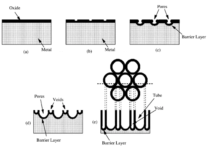
1.2.4 Pore formation in porous AAO films
In the recent years, much attention has been paid to porous AAO films rather than the
highly ordered pores were obtained 40 years later.40
It is very interesting to know how the high density pores initiate and how the hemispherically
shaped pore bottom starts. The initiation and growth of pores are associated with accelerated
dissolution of aluminium oxide with the influence of electric field.37 More detailed
investigations25,39 suggested that electropolishing or other pretreatment could leave a slightly
scalloped surface of aluminium covered by an oxide coating layer. A scalloped “native” barrier
oxide film grew over this scalloped surface; as anodisation started, pores would start at cracks
and imperfections in the surface, leaving an electric field concentrated below the regions where
the oxide film was thinner, thus aiding the local dissolution of oxide.
It is also suggested that during early growth, the film on ridges and protuberances becomes
thicker than in the depressions. Ions move through oxide more easily at these locations because
of higher film stress, impurities, or oxide flaws, and so the current concentrates at these locations.
As the oxide acquires more uniform properties, the current will shift towards the thinner oxide in
depressions. Because of the concave geometry that has developed, there is a slightly higher
electric field in depressions, and field-assisted dissolution promotes local oxide thinning and
current concentration. This initiates pores, and the pore size, density, and distribution adjust until
a steady state prevails. Both these cases sound reasonable.
The problem is the cracks on the surface of the air-formed oxide layer, protuberances and the
ridges seem not enough to form initially such dense pores at the entire surface, typically
1010/cm-2.48. Electropolishing can create pit sizes from a few to tens of nanometers and a pit
density of about 1010-1012/cm-2, some of which can develop into pore nuclei.39 Anodisation
without any pretreatment can also achieve well ordered porous alumina structure.
These initiatory pores compete with each other, only the survivors developing into the major
pores. As the anodising continues, the metal/oxide interface moves into the metal, and the pores
grow at the equilibrium of dissolution and oxidation taking place at the both sides of the oxide.
The anodic film thickens with increasing time, while cell and pore diameters retain a constant
value.
The well accepted concept for the formation of porous anodic metal oxides is based on the
competition between the field-assisted oxide dissolution at the electrolyte/oxide interface and the
high field is present, the Al-O bond of the alumina is lengthened and weakened due to the
polarization. It will then be easier for the H+ions in the electrolyte to react with and dissolve it.
However, this field-dissolution process has been questioned by recent authors,82 who explained
the growth of anodic pores by the high plasticity of the anodic alumina in the barrier region in
the presence of ionic transport, with film growth stresses displacing material from the barrier
layer towards the cell wall region during anodising.
Figure 1-4. Schematic representation of the field-assisted dissolution of A12O3, (a) before
polarization, (b) after polarization, (c) removal of A13+and O2-ions, and (d) the remaining oxide.
(By O’Sullivanet al, 1970)25
1.2.5 Self-ordering of pores in porous AAO films
Since the pores generate based on the pits left by electropolishing or on the defects on the
substrate surface, usually they appear as an irregular and disordered structure at the early stage of
Al anodisation. Close packed AAO pore arrays with perfect hexagonally ordered pattern could
be achieved by prolonged anodisation due to the self-organisation mechanism during films
growth.
When suitable anodisation voltage and electrolyte are used, hexagonal ordered pores can be
easily produced in AAO films. Perfect hexagonal anodic alumina pore arrays with a very narrow
size distribution and extremely high aspect ratios over an area of a micrometer scale were grown
would grow as the anodisation prolonged. Li et al48 found in their experiments that the average
ordered hexagonal domain area was a linear function of the time.48 These revealed a structure
rearrangement process during the anodisation. The prolonged anodisation will tend to turn a
larger area into hexagonal ordering. Later, by analysing a series of porous alumina structure
prepared under different anodisation time, Nielschet al84 showed that the domain size does not
linearly increase with time but has a maximum (Figure 1-5). The reason the domain size
decreased after a critical time was explained as an aberration from the 10% porosity rule due to a
change of the pH value at the pore tip after lengthy anodisation. If this argument is correct, a
larger electrochemical cell would maintain the properties of the electrolyte unchanged and the
drop of the domain size would not be observed.
Figure 1-5. (left axis) Average domain size as a function of the anodisation time in 1 wt %
H3PO4 at 195V. The domain size is obtained by numerical picture treatment. First the domain
size increases due to self-ordering, but after a critical time shown by the dashed line the domain
size decreases again. (right axis) Current transient during of the same sample, showing first a
current decrease typical for self-ordering, and then after a critical time the current increases. (By
Nielschet al, 2002)84
Singh et al76 attributed the pore initiation and self organisation of the porous structures in
aluminium oxide films at the initial stage to the significant elastic stress in the oxide layer. The
dependence of the current on the overpotential and a dependence of the activation energies of the
oxide-electrolyte interfacial reactions on the Laplace pressure and the elastic stress in the oxide
layer. In the case when the effect of elastic stress is negligible, a weakly nonlinear analysis leads
to formation of spatially irregular pore arrays that have been observed in experiments. In the case
when the effect of elastic stress in the oxide layer is significant, the instability can transform
from a long-wave type to a short-wave type. A weakly nonlinear analysis of the short-wave
instability shows that it leads to the growth of spatially regular, hexagonally ordered pore arrays.
Figure 1-6.Simulation of the pore formation in AAO via a weakly nonlinear analysis. (a) When
the elastic stress in the oxide layer is negligible, the simulation leads to irregular pore array. (b)
When the effect of elastic stress is significant, regular pores array could be achieved. (By Singh
et al, 2006)76
This theoretical framework studied the morphological evolution as well as the role of stress in
the formation of AAO films. However, as pointed out by the authors, this model is valid only for
the initial stages of instability leading to pore initiation and self organisation. It could not explain
the self-adjustment process as the pores grow in depth, which is considered to be the most
important factor determining the ordering of the AAO arrays.
Vorobyovaet al77 considered distribution of an applied voltage in three main components of
an electrochemical bath system: a growing oxide layer; a Helmholtz layer at the electrolyte/oxide
interface; and a Gouy–Chapman space charge layer, which extends to the quasi-neutral
self-organisation ion concentration distribution in the Gouy–Chapman layer, leading to a growth
of highly ordered pores as shown in Figure 1-7. The cell size of the porous oxide was shown to
vary as Gouy–Chapman layer thickness, which depends on the temperature, concentration, and
composition of the electrolyte. It was believed that pores do not start to nucleate simultaneously
across the entire surface, but do so at energetically favorable sites where most ion transfer occurs.
This charge distribution model accounts for the highly ordered pore patterns at the initial
anodising stage, but could not explain the self-adjustment between pores. Moreover, as observed
experimentally, random distributed pores or at most poor ordering pore patterns could be
observed at the beginning of the anodisation of aluminium. Only after adjustment for a sufficient
long time for the initial pores, satisfactory ordering could be achieved.
Figure 1-7. Formation of hexagonal spatial pattern of ion concentration in a Gouy–Chapman
layer. The vertical axis represents normalized concentration; the horizontal axes are for
coordinates (in nanometers) along the surface being anodised. (By Vorobyovaet al, 2007)77
The principle of the pore ordering has been investigated extensively by a number of
groups,25,27,40,76-78,85-87 while the most commonly accepted model is based on mechanical stress
during the oxidation process.27,82 The ionic density of Al3+ in anodic alumina (3.66×10²²/cm3)
corresponding to the weight density of approximately883.1 g/cm3 is significantly lower than the
atomic density of aluminium metal of 6.02×10²²/cm3. The oxidation of aluminium during the
anodisation may lead to significant volume expansion at an elevated anodising voltage due to
expansion during oxide formation at the oxide/metal interface could be a possible origin of a
repulsive force between neighboring pores. Jessensky et al27 proposed that this repulsive force
could account for the self-organised formation of hexagonal pore arrays. It was also suggested
that neither too large nor too small expansion would result in a long range ordering of the pores.
Only a medium volume expansion of 1.2 times from aluminium to alumina, independent of the
specific anodisation conditions, could lead to an ordering.89 This empirical model implies that
the mechanical stress plays an important role in the self-organised process. However, it is unclear
how the repulsive force, which can be either positive or negative, works in detail. As well as the
detailed adjusting process, many experimental observations such as the generation of the pores,
the formation of the hemispherical pore bottom, and the merging and splitting of the pores, still
cannot be explained by the repulsion model.
Further to the mechanical stress model, a 10% porosity rule was proposed by Nielschet al.84
However, by using the so-called hard-anodisation process, Leeet al70recently successfully made
well ordered hexagonal pore arrays with a large aspect ratio and a porosity of 3.3%, which was
far below the 10% rule. This put the 10% porosity rule in question.
Figure 1-8. (a) Expansion of aluminium during anodic oxidation. (b) Alumina layer thickness
compared to the consumed aluminium layer using 20 wt. % H2SO4at 1 °C. (By Jessenskyet al,
1998)27
changes significantly with the applied voltage.24,25,70,90 For example, measured from large-area
hexagonal pore arrays, an interpore distance (Dint) = 63 nm when sulphuric acid (H2SO4) was
used as electrolyte and working voltage was 25 V;84,89Dint= 100 nm when oxalic acid (H2C2O4)
was used as electrolyte and voltage was 40 V;40,84Dint= 90-140 nm with an aged sulphuric acid
solution, a high anodisation potential up to 70 V and a high current density up to 200 mA/cm2;91
Dint = 220-300 nm with oxalic acid at 110-150 V;70 Dint = 500 nm when applying phosphoric
acid (H3PO4) and 195 V.84,92
On the other hand, the porosity of AAO films seems to be insensitive with the applied voltage.
Nielschet al84proposed an empirical 10% porosity rule independent of the specific anodization.
However this model was in contradiction with some other reports70,93,94
O’Sullivanet al25thought that the pore and cell diameters should be largely independent of the
type of electrolyte, and depend mainly on the applied voltage. They gave a typical cell growth
ratio of 2.5 nm/V, independent of electrolytes used. It seems that the electrolyte type and other
factors such as the temperature and current density will not affect the cell voltage ratio or at most
at a neglectable minor level. However, it has been reported very recently that the cell voltage
ratio was found to be 2 nm/V (20% smaller than 2.5 nm/V) in the hard anodisation of the
aluminium by Leeet al.70
Moreover in the research of aluminium anodised in sulfuric acid by Chu et al,91 the
corresponding anodic ratio of cell diameter (nm/V) demonstrate a reverse relation to anodising
potential, from 4.4 nm/V at 8 V to 1.8 nm/V at 70 V, which is so significant that other factors
rather than the voltage affecting the cell dimension must be taken into account. The authors
described this phenomenon as due to the interacting repulsive force between the alumina cells
which is associated with the expansion during oxide formation at the aluminium/oxide interface.
This explanation is not sufficiently convincing, since the repulsive force between cells may
change the dimension of a single cell, but it could not change the whole average dimension of
the cells. Therefore, the cell dimension doesn’t depend solely on the voltage, and the cell/voltage
ratio could vary significantly with a change of the anodising voltage.
1.3 Anodic titanium oxide
unique advantages in the applications such as catalysis or batteries due to the high surface area or
short solid state diffusion paths.95,96As a result, considerable research efforts worldwide focus on
the design and synthesis of novel nanostructures of the transition metal oxide via chemical or
electrochemical approaches. Among all transition metal oxides, TiO2 attracted the most interest
by far due to its unique functional properties and wide potential application. Titania
nanostructures have been successfully produced by template based, hydrothermal, and sol–gel
methods.97-99In the past decade, self-ordered titanium oxide films produced by anodisation of Ti
metal have attracted intense interest from scientists and chemists all over the world.
The most significant difference between typical anodic titanium oxide (ATO) and anodic
aluminium oxide (AAO) is that the latter is a continuous film with a pore array while the former
consists of separated nanotubes. Several recent studies have showed that titania nanotubes have
better properties compared to many other forms of titania for applications in photocatalysis,100,101
gas sensors,102-105photoelectrolysis,22,106,107and photovoltaics.23,108-110
As initially reported by Gonget al28 in 2001, the first generation of titania nanotubular arrays
fabricated by anodisation using an aqueous HF-based electrolyte could achieve a length of about
500 nm.28The nanotube-array length was subsequently increased to about 7μm by control of the
anodisation electrolyte pH (higher values while remaining acidic) which reduced the chemical
dissolution of TiO2 during anodisation.29 Pauloseet al30 reported a new generation of vertically
oriented TiO2 nanotubes with lengths up to 134 μm, by the use of various nonaqueous organic
electrolytes. Meanwhile the ordering of the ATO nanotubes has also been improved dramatically.
Accompanied by significant progress in the fabrication of TiO2 nanotubes via the anodisation
method, scientists and chemists also made great efforts on the mechanism of the formation and
self-organisation of the tube arrays.
1.3.1 Fabrication of ATO nanotubes
Like the anodising of aluminium, barrier-type and porous-type anodic titanium oxide films
could be obtained depending on the electrolytes used. Barrier-type anodic titanium oxide films
could be formed when titanium metal was anodised in sulphuric acid. Anodisation of Ti is
widely investigated in sulfuric acid at voltages typically up to approximately 100 V. Under these
exact breakdown voltage, however, depends on the exact experimental parameters (e.g., the
electrochemical parameters of anodisation). For oxide films formed below the breakdown
voltage, typically a growth rate of 2.5 nm/V has been reported.114,115 The structure of the oxide
films has typically been reported to be amorphous at low voltages (below 20 V112, and
crystallisation takes place at higher voltages. Depending on the anodising conditions, the crystal
structure has been reported to be anatase,114-117a mixture of anatase and rutile,114,118or rutile.114
For producing ATO nanotubes, several different electrolytes have been used so far. Therein,
the most investigated electrolytes are fluoride solutions. Gong et al28 reported their ATO
preparation in a 0.5 wt% HF aqueous solution at room temperature using different anodising
voltages, from 3 to 20 V. Figure 1-9 shows SEM images of a typical ATO sample. Appearance
of separated nanotubes became obvious at an anodising voltage of 20 V.
Figure 1-9.FE-SEM top view (a), cross sectional (b), and bottom view images of titanium oxide
nanotubes anodised in 0.5 wt% HF solution at 20 V for 20 min. (By Gonget al, 2001)28
It was noticed that the film thickness could not be increased further from 400-500 nm using a
HF-based electrolyte. Fluoride solution can help to dissolve TiO2 by forming [TiF6]2− anions.
However, too strong acidity of the HF-solution results in an over fast dissolution rate of the
formed TiO2nanotubes. Mixture with other acids did not help very much, but the quality of the
nanotubular arrays could be varied. Moret al103,119 reported that addition of acetic acid to a 0.5
wt% HF electrolyte in a 1:7 ratio resulted in more mechanically robust nanotubes without
changing their shape and size. Ruan et al120 found that the surface morphology of nanotubular
arrays anodised in an electrolyte containing 2.5% HNO3 and 1% HF at 20 V for 4 h showed a
uniform, clean, regular nanotube structure with a length about 400 nm, while an electrolyte of
irregularity, with a nanotube length about 560 nm. Beranek et al121 anodised titanium in H2SO4
electrolytes containing low concentrations of HF (0.05-0.4wt %). It was found that under
optimized electrolyte conditions, highly ordered porous TiO2 that consists of pore arrays with a
single pore diameter of 140 nm and a pore spacing of 150 nm with a limiting thickness of 500
nm could be obtained.
When using a KF or NaF solution as an electrolyte, the thickness of ATO films can be
significantly increased.122 The acidity of the electrolyte might be tuned by adding HF, H2SO4or
Na2SO4 in order to adjust the balance of dissociation of titania at the electrolyte/oxide interface
and oxidation of titanium at the oxide/metal interface.121,123 The better electrolyte is probably a
NH4F-based solution. From a mixed solution of NH4SO4 and NH4F, the ATO film can grow up
to several micrometers in thickness.29
Considering diffusion as the main effect on local acidification,29 Macak et al42 demonstrated
an ATO sample prepared in a glycerol electrolyte with 0.5 wt% NH4F with a length of 7µm and
a high degree of regularity and homogeneity as shown in Figure 1-10.
Figure 1-10. SEM images of smooth ATO with a length of 7µm produced in a glycerol
electrolyte with 0.5 wt% NH4F: (a) top view; (b) bottom view; (c) cross sectional view. The inset
of (c) shows the walls of the nanotubes in more details. (d) Top view of an anodised sample after
removal of some nanotubes. (By Macaket al, 2005)42
co-workers30,124 obtained nanotubular arrays up to approximately 220 µm in length using a
variety of organic electrolytes including dimethyl sulfoxide (DMSO), formamide (FA), ethylene
glycol, and N-methylformamide (NMF) (Figure 1-11). It was suggested that, the key to
successfully achieving very long nanotubular arrays was to minimize water content in the
anodisation bath to less than 5%. With organic electrolytes, donation of oxygen is more difficult
in comparison with water, thus reducing the tendency to form oxide125 and slowing down the
process of the nanotube growth. At the same time, the reduction in the water content reduces the
chemical dissolution of the oxide in the fluorine containing electrolytes and hence aids the
longer-nanotube formation.
Figure 1-11.FESEM cross-sectional (a), bottom (b), and top (c) images of an ATO grown at 60
V in an ethylene glycol electrolyte containing 0.25 wt% NH4F. (By Shankaret al, 2007)124
In fact, ATO nanotubes could also be obtained by anodising titanium metal in fluoride free
electrolytes. In 2005, Nakayama et al126 reported that titania nanotubes can be obtained by
anodisation in a perchloric acid solution. Hypothesizing that chlorine ions could perhaps play a
role similar to that of fluorine ions during the anodisation of titanium, Richter et al127
synthesized high-aspect-ratio titania nanotubes by the anodisation of titanium in chlorine and
oxalic acid containing electrolytes. Chlorine-based anodisation has an advantage over the techniques mentioned above in that it can grow long titania nanotubes (up to 60 μm) in a very
short time (growth rate is >1000 times faster than in fluorine media; e.g., 10 min in chlorine-based electrolytes compared to 17 h in fluorine-based electrolytes for 60- and 7-μm
nanotubes, respectively). Later, Richteret al128fabricated the ATO films in formic acid-, oxalic
electrolytes, suggesting that the chemistry for nanotube formation is versatile with regard to the
[image:31.595.110.526.138.371.2]acid used (Figure 1-12).
Figure 1-12.SEM images showing various types and degrees of ordering of the titanium oxide
nanotubes. The specific experimental conditions are not necessarily related to the morphology
depicted. (a) Totally disordered agglomerations of relatively short (<500 nm) nanotubes (0.5 M
formic acid, 15.5 V). (b) Highly disordered agglomerations of long nanotubes (0.5 M gluconic
acid, 13 V). (c) Loosely packed nanotubes with one preferred direction, allowing the formation
of bundles (0.5 M gluconic acid, 12 V). (d) Tightly packed nanotubes with one preferred
direction, allowing the formation of grains (0.5 M trichloroacetic acid, 14V). (e) Tightly packed
nanotubes with two perpendicular preferred directions, allowing the formation of interwoven
bundles (0.5 M formic acid, 15.5 V). (f) Top view of a bundle clearly showing the tubular aspect
of the constituents (0.02 M hydrochloric acid, 18 V). (By Richteret al, 2007)128
1.3.2 Formation mechanism of ATO nanotubes
According to Grimes’ group,129 the key processes responsible for anodic formation of titania
should be the same as anodic alumina: (1) Oxide growth at the surface of the metal occurs due to
anions migrate through the oxide layer reaching the metal/oxide interface where they react with
the metal. (2) Metal ion (Ti4+) migration from the metal at the metal/oxide interface; Ti4+cations
will be ejected from the metal/oxide interface under application of an electric field. (3) Field
assisted dissolution of the oxide at the oxide/electrolyte interface. Due to the applied electric
field the Ti–O bond undergoes polarization and is weakened, promoting dissolution of the metal
cations.
Ti4+ cations dissolve into the electrolyte, and the free O2- anions migrate towards the
metal/oxide interface, to interact with the metal. The overall reactions for anodic oxidation of
titanium can be represented as
H2O → O2-+ 2H+ (1.7)
Ti + 2O2- → TiO2+ 4e- (1.8)
In the initial stages of the anodisation process field-assisted dissolution dominates chemical
dissolution due to the relatively large electric field across the thin oxide layer. Small pits formed
due to the localized dissolution of the oxide, represented by the following reaction, act as pore
forming centers:22
TiO2+ 6F-+ 4H+ → [TiF6]2-+ 2H2O (1.9)
Then, these pits convert into bigger pores and the pore density increases. After that, the pores
spread uniformly over the surface. The pore growth occurs due to the inward movement of the
oxide layer at the pore bottom (barrier layer) due to processes (1.7)–(1.9).129
As the pores become deeper, the electric field in the protruded metallic region between pores
increases, enhancing the field-assisted oxide growth and oxide dissolution. Subsequently
inter-pore voids start forming as illustrated in Figure 1-13d. Thereafter, both voids and tubes
grow in equilibrium. Close examination of FE-SEM images show the formation of small pits in
Figure 1-13.Schematic diagram of the evolution of a nanotubular array at constant anodisation
voltage: (a) oxide layer formation, (b) pit formation on the oxide layer, (c) growth of the pit into
scallop shaped pores, (d) metallic part between the pores undergoes oxidation and field assisted
dissolution, and (e) fully developed nanotubular array with a corresponding top view. (By Moret
al, 2006)129
The above growth mechanism proposed by the Grime’s group attributed the formation of ATO
nanopores array to the electric field driven oxidation of titanium metal base and electric field
enhanced dissolution of titanium oxide like the AAO case. The separation of ATO pores was
attributed to the inter-pore voids which form at the enhancing the field-assisted oxide growth and
oxide dissolution in the protruded metallic regions between pores. This mechanism could well
explain the formation and growth of ATO pores though the self-organisation phenomenon of the
ordered pores array was not elucidated. The voids growth mechanism seems imperfect in
elucidating the separation of ATO pores. Due to the field enhanced oxidation and dissolution,
there will be small new pores generated at the bottom of these voids. And secondary new voids
will form in the joint areas between the large pores and the new pores. Therefore, this
mechanism should be modified in some aspects.
However, Macak et al29, 42 believed the mechanism of pore formation in titanium anodisation
the .electric-field-aided ion transport. As the dissolution rate of titanium oxide greatly depends
on the local acidification in fluoride containing electrolyte, the anodic pores grow in the higher
acidification at the pore bottom than the pore mouth.29
This model has been improved by the same group130 and was described as follows (Figure
1-14): in the very early stages a compact titanium oxide (and hydroxide) layer grows, then
dissolution and breakdown of the barrier oxide film occurs on random sites of the surface, which
act as seeds of the growth of a disordered worm-like structure underneath the remaining compact
layer. A pH gradient is developed between the tips and the bottoms of pores where the lower pH
at bottom leads to an accelerated TiO2dissolution and pore penetration into the Ti substrate.29
Only if the current in a pore is sufficiently high it will “survive”; thus under a critical value the
pore growth is “shut down”, which naturally facilitates the transition from irregular to regular
[image:34.595.188.448.373.662.2]pores.
Figure 1-14. Schematic representation of the TiO2 nanotubular arrays formation: (a) compact
layer growth to the maximum thickness, (b) breakdown of the barrier film, (c) growth of the
pores resulting in a worm-like structure, (d) more ordered structure partially covered with the
In this improved model, the chemical dissolution of titanium oxide was considered to be a
dominant factor compared to the AAO case. And the dissolution rate of titanium oxide was found
to greatly depend on the local acidification in fluoride containing electrolytes. Subsequently the
pH gradient in the ATO tubes leads to an increase of the length of anodic nanotubes. Besides, the
existence of titanium hydroxide during the formation of ATO was confirmed by an XPS study.
However, this model still cannot explain the regular shape and ordering of the pores at the early
stage of anodisation. In addition, it is also difficult to explain the formation of the gap between
the nanotubes using this model.
1.4 Other anodic metal oxides
To date, there are a number of other metals have been tried to produce porous oxide films.
Hexagonal porous anodic metal oxide structures have been achieved in some of these metals.
The anodising ratio varies from 1.60 nm/V to 2.20 nm/V.47
1.4.1 Anodisation of hafnium
Hafnium oxide has many interesting properties, e.g., its good chemical stability and thermal
stability, high refractive index and relatively high dielectric constant.131,132 These properties
make hafnium oxide a valuable material to be used as a protective coating, optical coating, gas
sensor or capacitor.133-137Self-organised porous hafnium oxide layers were obtained successfully
for the first time by Tsuchiya and Schmuki31via anodisation of hafnium at about 50 V in 1 M
H2SO4+ 0.2 wt% NaF at room temperature as shown in Figure 1-15. Anodisation potential was
found to be a key factor affecting the morphology and the structure of the porous oxide. The pore
diameter was found to increase with increasing potential. Porous hafnium oxide layers with high
Figure 1-15. Plan-view (a) and bottom-view (b) FE-SEM images of anodic porous hafnium
oxide layers formed at 50 V in 1 M H2SO4+ 0.2 wt% NaF at room temperature. (By Tsuchiyaet
al, 2005)31
1.4.2 Anodisation of niobium
Porous niobium oxide structures could be applied in gas sensors,138 catalysis,139and optical140
and electrochromic141 devices. Anodisation of niobium has been studied in various
electrolytes.142,143 Self-organised porous anodic niobium oxide films were successfully obtained
by Sieber et al32 and Karlinsey et al144 in 1 M H2SO4 + 1 wt% HF and 1.5% HF respectively.
More recently Choiet al145obtained anodic Nb2O5films with an effective thickness over 500 nm,
consisting of a protective outer layer of around 90–130 nm and an inner layer of 300–400 nm,
via an optimized anodisation–annealing–anodisation process (Figure 1-16).
Figure 1-16.FE-SEM images showing top view (a) and sectional profile (b) of porous niobium
oxides prepared in 1 wt% HF + 1 M H3PO4by anodisation–annealing–anodisation process. (By
A stress determined formation mechanism was proposed for anodisation of niobium by Zhao
et al.146 Since the density of niobium in niobium pentoxide is much smaller than that of the
niobium metal, oxidation of niobium metal yields an increase of inner stress in the oxide layer.
As the inner stress increases, niobium oxide expands outside to form bulges and facilitates the
oxidation of niobium metal under beneath, leading the formation of microcones. If no bulges are
generated, the inner stress would break the oxide layer, leading to the growth of microcones.
1.4.3 Anodisation of tantalum
Ta2O5 has attracted intensive attention due to its application in optical devices, and as a
protective coating material for chemical equipment, or suitable material for storage
capacitors.147-151 Anodisation of tantalum has been widely investigated in sulfuric, phosphoric
acid, and Na2SO4 solutions, and a layer of amorphous Ta2O5 with a uniform thickness could be
obtained.143,152 Self-organised porous anodic tantalum oxide with a reasonably narrow size
distribution was fabricated by Sieberet al33,153 via anodising tantalum in 1 M H2SO4 + 2 wt %
HF for 2 h after a potential ramp from open-circuit potential to 20 V with a sweep rate 100 mV/s.
Figure 1-17.SEM top views (a) and cross sections (b) of anodic Ta2O5prepared in 1 M H2SO4+
2 wt % HF for 2 h after a potential ramp from the open-circuit to 20 V with a sweep rate 100 mV
s−1. (By Sieberet al, 2005)153
1.4.4 Anodisation of tungsten
Tungsten oxide (WO3) has been receiving considerable attention in recent years for its use in
research in nonporous anodic tungsten oxide films,165-167nanoporous anodic tungsten oxide was
obtained by galvanostatic anodisation in oxalic acid by Mukherjeeet al34, although the regularity
of the pores appeared to be rather poor. Since then several groups have made a good progress to
some extent in controlling the morphology and ordering of the anodic tungsten oxide.168-170For
example, de Tacconiet al170reported that porous anodic WO3made in 0.3 M oxalic acid for 1 h
at 35 V showed dense pores with a small pore size distribution as shown in Figure 1-18.
Figure 1-18. SEM image showing morphologies of nanoporous anodic WO3 films prepared in
0.3 M oxalic acid for 1 h at (a) 10 V, (b) 35 V. (By De Tacconiet al, 2006)170
1.4.5 Anodisation of vanadium
Glacial acetic acid with small percentages of water and sodium tetraborate has been found
to be the most suitable electrolyte for anodisation of vanadium.171-173 Due to the existence of the
unfilleddshell, the phase composition of the anodic vanadium oxide could be rather complicated,
such as V2O5,174-177 VO2,171,178,179 or a mixture of V2O5 and other oxide phases with lower
oxidation states.177,180–182
1.4.6 Anodisation of zirconium
Zirconium oxide is an important functional material that plays a key role as an industrial
of up to several hundred nanometers in thickness can be achieved in many electrolytes.185 A
unique feature in comparison with other anodic metal oxides mentioned above is that the growth
of the compact ZrO2 layer at room temperature directly leads to a crystalline film186 rather than
an amorphous film as observed from other anodic metal oxides. Formation of self-organised
porous zirconium oxide layers produced by anodisation of Zr at 30 V in an electrolyte of 1 M
H2SO4+ 0.2 wt% NH4F was reported by Tsuchiyaet al.36,187
Figure 1-19. SEM images of anodic porous zirconium oxide layers. a) Plan view and b)
cross-sectional view of the porous layer formed in 1 M H2SO4+ 0.2 wt% NH4F electrolyte at 30
V for 5 h at 200C. (By Tsuchiyaet al, 2005)36
1.5 Applications of porous AAO and ATO
As being the two most investigated anodic metal oxides, AAO nanopores films and ATO
nanotubes arrays have been widely applied in laboratory research and commercial industry.
Though in this dissertation we focus on the formation mechanism of self-organised highly
ordered AAO and ATO anodic films, and the physical chemistry involved in the anodisation
process, we would like to review some typical applications of AAO and ATO in this section.
1.5.1 Application of porous anodic aluminium oxide
Non-porous anodic alumina films have been widely applied in the prevention and decoration
self-organised porous AAO with perfect hexagonal pore patterns has been used to as a template
to fabricate a variety of nanomaterials, such as nanoparticles, nanowires and
nanotubes.14-19,71-74,197 Some typical applications of AAO include: etching masks for
semiconductor substrate,14-16 pattern transfer by replica of AAO as a template,40 and deposition
of functional materials by chemical vapor deposition (CVD) or electrochemical deposition
method.17,18,198-203
Etching mask for semiconductor substrate
Pattern transfer of AAO nanochannels to a semiconductor substrate is promising for
applications such as photonic band materials, field emitter arrays and quantum dot arrays. A
typical method proposed by Shingubara et al16uses a porous alumina film deposited directly on
the semiconductor substrate. A thin porous AAO film with an aspect ratio below 5 was formed
on a Si/SiO2substrate from sputtered aluminium. Reactive ion etching using chlorine with a high
self-bias of RF plasma proved effective for pattern transfer to Si.
Pattern transfer by replica of porous alumina as a template
Pattern transfer of AAO nanohole arrays to metallic hole arrays using a replica was firstly
proposed by Masudaet al40 in 1995. First, a negative nanohole array pattern was transferred to
poly methyl methacrylate (PMMA) by coating it on the porous alumina film. Then, the porous
AAO film was chemically wet-etched, leaving behind only the resist PMMA pattern, which can
be used to form a replica by deposition of metals. Yanagishitaet al204reported a synthesis of Ni
nanohole arrays using a two-step replication of AAO template (Figure 1-20).
An AAO film with through-holes was dipped in a methyl methacrylate (MMA) monomer with
5 wt% benzoyl peroxide as an initiator for polymerization. After polymerization by UV
irradiation, the sample was polished to expose the two sides of the embedded AAO membrane. A
thin Pt-Pd layer was coated onto the surface of the sample by sputtering, and then a Au
reinforcing layer, which acted as an electrode for the metal deposition of hole array materials,
was formed electrochemically. After the formation of the Au electrode, the alumina membrane
was dissolved in 10 wt% NaOH for 50 h to form the negative PMMA structures.
the negative PMMA. A Ni hole array was obtained by dissolving the PMMA nanopillars in
[image:41.595.145.495.147.417.2]chloroform (Figure 1-20c).
Figure 1-20. (a) Schematic for the preparation of metal nanohole arrays: 1) the AAO film is
embedded in PMMA, 2) exposure of two sides of AAO, 3) formation of electrodes for
electrochemical deposition of metal, 4) removal of AAO template, 5) electrochemical deposition
of Ni, and 6) removal of the PMMA negative. (b) SEM image of the PMMA nanopillar array
after removing the alumina template. (c) Cross-sectional SEM image of a Ni hole array
membrane. (By Yanagishitaet al, 2005)204
CVD deposition on AAO template
Chemical vapor deposition (CVD) as a common method to produce high-purity,
high-performance solid materials has been extensively used to synthesize nanomaterials in AAO
templates in recent years.74,203
Silicon nanowires and nanotubes could be grown via the chemical vapor deposition in the
AAO templates. The barrier layer of the AAO was etched in phosphoric acid at 30 °C for 90 min