Abstract —Algorithms for automatic analysis of the geometrical parameters of surface images obtained by scanning probe microscopy have been developed. The algorithms include calibration of linear displacements of the scanners using the image of the periodic linear reference samples (calibrating grids); calculation of the grain size distribution for nanostructured materials; the analysis of the geometrical parameters of the imprints and traces left after the surface deformation during scratch test and indentation. The descriptions of the algorithms are presented. The experimental data presented demonstrate the performance of the software modules based on the proposed algorithms.
Index Terms — Image processing, scanning probe microscopy, nanohardness tester, scratch tester.
I. INTRODUCTION
canning probe microscopy (SPM) is widely used in modern materials research because it is relatively easy to use and informative in terms of the surface analysis. The possibility to do surface imaging with resolution about 1 nm allows studying objects of different nature such as material nanostructure or the results of local surface deformation during mechanical properties testing. Such tasks as objects recognition, definition of the morphology and size, sorting on some of its parameters, statistical processing of the data are often come along with SPM imaging. The digital representation of the SPM data makes it possible to implement automatic analysis of the surface geometrical parameters. The presented algorithms are tested on the data sets obtained using scanning nanohardness tester NanoScan-3D developed in FSI TISNCM [1]. This device is combining the capabilities of scanning probe microscopes with techniques for surface modification and mechanical properties testing.
Manuscript received March 5, 2011; revised April 12, 2011. This work was supported by the Ministry of Education and Science of the Russian Federation, grant No. 2009-1.1-207-024-142.
N. Lvova is with Federal State Institution “Technological Institute for Superhard and Novel Carbon Materials” (FSI TISNCM), 7а, Centralnaya street, Troitsk, Moscow region, Russia 142190 (e-mail: [email protected]).
I. Shirokov is with Lomonosov Moscow State University, Faculty of Computational Mathematics and Cybernetics, GSP-1, 1-52, Leninskiye Gory, Moscow, Russia 119991 (e-mail: [email protected]).
A. Useinov is with FSI TISNCM (e-mail: [email protected]). K. Gogolinskiy is with FSI TISNCM (e-mail: [email protected]).
II. CALIBRATION OF LINEAR DISPLACEMENTS OF THE SCANNERS USING THE IMAGE OF PERIODIC LINEAR
REFERENCE SAMPLES (CALIBRATING GRIDS) The algorithm is intended for evaluation of the calibrating grid period over its SPM image. The comparison of the period estimated over the image with its nominal reference value allows performing calibration of scanner linear displacement at the nanometer range.
A. Algorithm for estimation of the calibrating grid step size
The input data is the surface image obtained as a result of sample scanning and stored as an array of numbers z(x,y), where z is a height of surface topography in the point, normalized to some fixed level; x, y are the Cartesian coordinates on the lateral plane. The coordinates x, y are set as points of the rectangular grid xy = xy,
{ , 0, 1,
x xi i Nx
x
i
x
0
h
xi
},
{ , 0, 1,
y yj j Ny
y
j
y
0
h
yj
}
. Here the grid steps hx and hy are constant but can be different from each other.The important feature of the presented algorithm is the independence of its operation on the angle of lateral rotation of the grid. This allows performing calibration in any direction. The recognition of the calibrating grid step boundary is done using the maximum value of the inclination angle of tangent lines to the scanned surface. The obtained points of maxima are approximated by straight lines using the least squares method. The positions of these lines show the steps boundaries on the grid image and are used for the subsequent evaluation of the step size. The algorithm also estimates the dependency of the step size from the coordinate x (or y), thus making possible to reveal the lateral nonlinearity of the scanners.
B. Algorithm operation results
Fig. 1a shows 2D image of the calibrating grid with the nominal period value of 3 micrometers and the step height 100 nm. Fig. 1b shows the positions of straight lines set which approximate the boundaries of the grid steps after algorithm operation. One can see on Fig 4a that grid period is increased with x and y increase. The maximum period value is 3.9 micrometers, the minimum value is 2.6 micrometers. To calibrate the scanner displacement in Y direction the average value should be used. The difference between the extreme and average values related to the image resolution in X and Y directions is the measure of scanner nonlinearity.
Surface Image Processing Algorithms in
Scanning Probe Microscopy and Nanohardness
Measurements
N. Lvova, I. Shirokov, A. Useinov, K. Gogolinskiy
Thus, the algorithm allows calibrating the scanner linear displacements in XY plane over two images of the calibrating grid obtained at different grid and scanner relative orientations. In practice, when the calibrating grid is installed in the device, the angle between its steps direction and X or Y scanner axis can reach up to 10 degrees, which leads to calibration error if not counted for. For the proposed algorithm the requirement of precise grid orientation is not critical. This feature allows increasing calibration accuracy and reducing calibration time.
III. CALCULATION OF THE GRAIN SIZE DISTRIBUTION FOR NANOSTRUCTURED MATERIAL
The size and the number of structural components is the important parameter of composite nanostructured material. The grain size distribution can be used for analysis of material physical and mechanical properties.
A. Grain recognition algorithm
Lets designate the values of grid function z in points (xi, yi) as z(i, j). The algorithm consists of several sequential steps. On the first step the point of maximum z(i, j) is estimated in XY plane. Then, the sections are built in every direction, for each section the point of minimum value along the section is estimated. The sections are built with use of the Bresenham algorithm. The minimum value along the section is estimated using criteria of zero first derivative of the section line. Thus, for every section the segment connecting the maximum z(i, j) and the local section minimum point is estimated. The average of all these segments lengths is calculated. Then all segments having length less than the average are rejected. The new average value is calculated over all left segments, this value is taken as a grain radius. The circle of the calculated radius and the center in the maximum point is drawn. The points inside the circle are marked and do not taken into account on future steps. Thus, the grain is approximated by the circle. The described procedure is repeated cyclically. The parts of XY plane covered by the marked circles are not considered. The algorithm finishes when the overall number of approximated grains reaches 1000 per square micrometer. The example of sections on 2D image is presented in Fig. 2.
B. Algorithm operation results
The proposed algorithm was applied for analysis of the nanocomposite material Al-C60 structure [2]. Fig. 3 shows
the intermediate result of the algorithm operation.
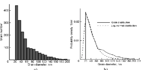
The grain number of 100 per square micrometer was used for the completion criteria. The grain number distribution as a function of diameter D is built using the array of estimated grain radii. Fig. 4a shows the corresponding diagram W(D): the height of the histogram bar represents the number of grains W with diameter within the left and right bounds of the bar.
a) b)
Fig. 1. (a) 2D-image of the calibrating grid with 3 mcm period and step height 100 nm; the size of scanning area is 20х20х0,1 mcm; (b) a set of straight lines approximating the edges of the calibrating grid as a result of the algorithm operation.
Fig. 2. Scheme of constructing the segments connecting the points of local maxima of z(i, j)function for the defined grains, with the boundary points of the scanned area.
a) b)
Fig. 3. (a) 3D SPM image of the nanocomposite Al-C60 surface, white colour notes the grains defined as a result of the algorithm operation, size of scanning area is 1,2х1,2х0,04 mcm; (b) corresponding 2D image of the grains.
a) b)
[image:2.595.324.535.43.219.2] [image:2.595.54.284.46.153.2] [image:2.595.313.561.393.503.2] [image:2.595.319.562.584.704.2]The minimum value D = 20 nm is limited by the measuring system resolution. Fig. 4b shows the dependence of the probability density for the distribution obtained after the algorithm operation (the solid line) and logarithmically normal distribution:
2
2
ln
2
1
exp
2
1
D
D
D
W
LThe arithmetic average diameter value calculated over all estimated grains is D0 = 57 nm, the values of distribution parameters are = 36 nm, = 0.6. One can see that both graphs coincide well with each other. The value of mathematical expectation Dav is calculated using the following equation:
2
exp
2
av
D
The obtained value is Dav = 52 nm. This appropriates well with the results of x-ray diffraction spectra analysis and transmitted electron microscopy data [2].
IV. CALCULATION OF GEOMETRICAL PARAMETERS OF SCRATCH TRACE
The scratch testing of the surface by the diamond indenter of different geometry is one of the most known and often applied techniques for materials mechanical properties testing. The scratch test is used for measuring hardness, wear resistance, fracture toughness at different length scales, including the nanometer scale [3,4,5]. Along with the scratching load the width and the depth of the scratch trace are also very important parameters of the technique. In particular, the width and the depth of the scratch are used for hardness and elastic recovery evaluation. The ratio of the scratch volume to the volume of material extruded to the surface is efficient characteristic for estimating Young’s modulus and wear resistance [6].
A. Algorithm for scratch parameters estimation
The proposed algorithm is intended for investigation of the following scratch parameters: recognition of scratch area; recognition of surface area elevated around the scratch trace; estimation of the average scratch width; calculation of the scratch volume; calculation of the volume of the material that was extruded above the surface level during scratch test. The scratch width is estimated using the sections perpendicular to the scratch direction; the boundary of the scratch is estimated using the tangent lines to the scratch cross section. The criterion for scratch boundary is some predefined tangent line angle. The scratch volume and extruded material volume (pile-up volume) are calculated as a sum of deviations of z(i, j) values from the average initial surface level line multiplied by the area of scanning grid cell. These values can be used for evaluation of mechanical properties of the material such as hardness, fracture toughness and wear resistance at the nanometer scale.
[image:3.595.305.539.185.289.2]B. Algorithm operation results
Fig. 5 to 7 presents application of the proposed algorithm
for estimation of the geometrical parameters of the scratch traces formed on fused silica, glass and titanium surface during scratch test. In these experiments both producing the scratches and subsequent imaging were done with use of scanning nanohardness tester NanoScan-3D. The measurement technique is described in details in [5].
The relation of scratch volume Vs to extruded material volume Vm as a function of hardness H and Young’s modulus E for materials investigated is listed in Table I.
TABLEI
MECHANICALPROPERTIESOFSAMPLESANDTHESCRATH PARAMETERSCALCULATIONRESULT
Sample
H
, GPaE
, GPaE
H
V
SV
MFused silica 9,5 70 9 0,1
Glass 7,1 90 13 0,2
Titanium 2,7 110 41 1,0
a) b)
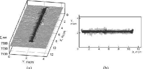
Fig. 5. (a) 3D SPM image of scratch on fused silica surface, size of scanned area is 6,0х5,0х0,1 mcm; (b) result of the program operation: dark colour notes the scratch area (total volume 0,24 mcm3), light grey colour – the pile-up area (total volume 0,02 mcm3).
(a) (b)
Fig. 6. (a) 3D SPM-image of scratch on glass surface, size of scanned area is 6,0х3,0х0,1 mcm; (b) result of the program operation: dark colour notes the scratch area (total volume 0,05 mcm3), light grey colour – the pile-up area (total volume 0,01 mcm3).
(a) (b)
[image:3.595.307.551.359.454.2] [image:3.595.309.554.520.639.2] [image:3.595.310.551.722.776.2]V. CALCULATION OF THE CONTACT AREA AT SCRATCH HARDNESS TEST
During the scratch hardness test using the three sided Berkovich diamond indenter hardness H is calculated as a relation of normal load P to the area of contact between the indenter and the surface. The contact surface is suggested to consist of two pyramid planes if scratch is performed “edge-forward” or of one pyramid plane in case of “face-“edge-forward” scratching [3]. In conventional scratch test the contact area is calculated from the suggested indenter geometry using the residual trace width which is estimated over the SPM image [1]:
2
b
kP
H
Here k is an indenter shape coefficient which is defined during calibration procedure on a reference material of known hardness. The height of plastic pile-ups along the scratch boundaries is considered to be constant for the whole area of contact between the indenter and the material. However, the real contact area differs from the calculated one due to the complicated geometry of pile-ups formed ahead the indenter as it moves forward during scratching.
A. Algorithm for the contact area projection calculation
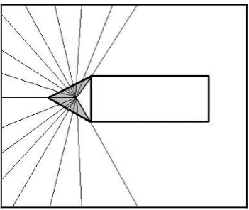
The proposed algorithm for the contact area calculation is based on the analysis of the residual scratch trace in its part corresponding to the moment of removing the indenter away from surface. The algorithm operation is based on building the set of sections starting from the conditional point of indentor apex contact with the material. The point belonging to the contact area boundary is defined as a maximum point z(x, y) along each section. Next step is estimation of array of z(x, y) values corresponding to the contact area and calculation of the area projected on XY plane. The projected area is calculated as a number of points multiplied by the scanning grid cell area. The calculated projected area value is used to evaluate the corrected hardness by scratch test. Fig. 8 shows the algorithm schema.
B. The algorithm operation results
The proposed algorithm for projected contact area calculation was applied for hardness evaluation for a number of materials with different physical and mechanical properties, such as nanocomposite material Al-C60, glass,
tungsten, silicon carbide. The values obtained were close to microhardness test results and also to the values obtained by the “residual imprint analysis” technique [7]. Fig. 9 presents the algorithm operation results for two of studied materials.
VI. ESTIMATION OF THE SIDE SURFACE AREA AND THE PROJECTED AREA OF INDENTATION IMPRINT
A. Algorithm for imprint area calculation
The feature of this task is the fact that the surface defined by function z(i, j) is curved due to the roughness effect. To calculate the common imprint parameters averaging should be applied. Lets define the average surface level Zav as the average value z(i, j) over the perimeter of the rectangular area as initial data. The imprint is considered to lie inside the specified rectangular area. Then it is necessary to estimate the minimum point of surface Zmin. This is supposed to be the maximum depth of indenter penetration inside the surface. Next step is estimation of the indentation area. In this purpose the set of sections is built starting from Zmin point and going to every point of the perimeter rectangular area. Every section should cross the imprint boundary since the Zmin point has position inside the imprint. The imprint boundary is defined on each section according to the following criteria: the value z(i, j) exceeds the Zav level. All points of the section are checked one by one starting from the Zmin. All section points from its beginning to the imprint boundary are considered as belonging to imprint area.
It is assumed that outside the imprint boundary pile-up surrounding the imprint is present. The pile-up area is estimated in the same way as the imprint area: the set of sections is built; each section starts from the Zmin point. In each point of the segment we define the angle between the tangent to the surface and the XY plane defined by Zav value. When this angle reaches the predefined value, the corresponding point of the section is considered as the pile-up top point. It is essential to set the limiting angle equal to zero, but the possibility to change it expands the algorithm
a) b)
Fig. 9. (a) Scratch on nanocomposite Al-C60 surface, load 5 mN, the projective contact area is (marked by dark colour) 1,47 mcm2, hardness value is 3,4 GPa; (b) scratch on glass surface, load 20 mN, the projective contact area (marked by dark colour) is 2,2 mcm2, hardness value is 8,0 GPa.
[image:4.595.309.547.180.294.2] [image:4.595.80.256.563.711.2]capabilities. Fig. 10 shows the scheme for building the segments and recognizing of the imprint boundary points.
B. Algorithm operation result
The results of algorithm application for projected contact area calculation for indentation in tungsten and glass are shown in Fig. 11 and 12 correspondingly.
The hardness value H was estimated using the flowing equation:
c
A
P
H
Here P is normal load applied to the indenter, Ac is the total projected contact area estimated with use of the presented algorithm. The hardness values obtained at submicrometer and nanometer scales are coinciding well with Vickers hardness.
VII.CORRECTION OF IMAGING DEFECTS CREATED DURING BUILDING THE IMAGE IN LINE-BY-LINE
SCANNING MODE
A. Algorithm for defects recognition and correction
The original algorithm is proposed which allows recognition and removal of some defects created during surface scanning [7]. These defects can appear if sample surface is very rough or if the scanning device is subjected to sudden mechanical vibrations. The imaging defect which is supposed to be removed looks like the “bad” line, for which values z(i, j) are significantly differ from the values of the neighboring line. Fig. 13a shows such defect as a sudden vertical ledge. In case of a single defective line the algorithm works as follows. The defective line is found using the line-by-line comparison and searching for the line where values z(i, j) differ significantly compared to corresponding points on the neighboring lines. Then the values z(i, j) of the defective line are replaced by the half-sum of the values from the neighboring lines. If the set of several defective lines is presented, the algorithm use more complicated criteria for replacement the points. The experiments have proved the reliable operation of the algorithm. It is capable of detecting the sets of defective lines looking similar to that on Fig.13a. Also, it does not change the values z(i, j) if
defects are missing. Fig. 13b shows the result of algorithm application to the image shown in Fig.13a. One can see that defective line was removed while all other data remain unchanged.
The proposed algorithm has several limitations. It cannot work correctly if the overall area of defective lines is too large. Also, it cannot find defects on the edges of the area being processed. Nevertheless, in the majority of practical situations the algorithm has proved to be useful at the surface scanned images processing of the various samples. Thus, an imprint with such defect can be used for hardness evaluation. This allows avoiding repeated experiments and reducing measurements time without decrease in their accuracy.
a) b)
Fig. 10. (a) Scheme of construction of the segments connecting the minimum point (marked by a dagger) with the boundary points of the scanned area; (b) illustration of pile-up boundaries definition around the residual print by variation of the limiting angle between tangents to the surface and horizontal plane. Arrows designate the points of pile-up borders at change of the limiting (predefined) value of the tangent inclination angle.
a) b)
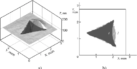
Fig. 11. (a) 3D SPM image of indentaion in tungstin, size of scanned area is 2,8х3,2х0,2 mcm; (b) result of the total projected area calculation. The imprint projection consists of the indent area (1) and pile-up areas (2). The calculated hardness value is 7 GPa.
a) b)
Fig. 12. (a) 3D SPM-image indentation in glass, size of scanned area is 2,8х3,1х0,2 mcm; (b) result of the total projected area calculation. The imprint projection consists of the indent area (1) and pile-up areas (2). The calculated hardness value is 6 GPa.
a) b)
[image:5.595.51.288.86.199.2] [image:5.595.50.284.342.471.2] [image:5.595.312.546.444.572.2] [image:5.595.51.287.539.658.2]VIII. CONCLUSION
The algorithm of residual imprint projected area calculation for indentation and scratch test has been developed. The experimental verification of the algorithm application to hardness evaluation at the nanometer scale for material with different mechanical properties has been carried out. The grain recognition algorithm for image of nanostructured material surface allows estimating the parameters of the grain size distribution. The algorithm of scanning defects correction allows reducing the number of tests for obtaining the statistically significant measurement results and improving the measurement accuracy. The algorithm of scanner linear displacements calibration can be applied for estimation of the non-linearity in scanning probe devices performance.
ACKNOWLEDGMENT
The authors would like to thank Professor V. D. Blank for his interest to this study and useful discussions.
REFERENCES
[1] A. Useinov, K. Gogolinskiy, V. Reshetov, “Mutual consistency of hardness testing at micro- and nanometer scales”, Int. J. Mat. Res., vol. 2009, pp. 968-972, 2009.
[2] M. Popov, V. Medvedev, V. Blank, V. Denisov, A. Kirichenko, E. Tat’yanin, V. Aksenenkov, S. Perfilov, V. Lomakin, E. D’yakov, and V. Zaitsev, “Fulleride of aluminium nanoclasters”, J. Appl. Phys., vol. 108, pp. 094317 1-6, 2010.
[3] V. K. Grigorovich, Hardness and microhardness of metals. Moscow: Nauka, 1976, ch.7, in Russian.
[4] J. A. Williams, “Analytical models of scrath hardness”, Trybology International, vol. 29, pp. 675-694, 1996.
[5] V. Blank, M. Popov, N. Lvova, K. Gogolynsky, V. Reshetov, “Nano-sclerometry measurements of superhard materials and diamond hardness using scanning force microscope with the ultrahard fullerite C60 tip”, J. Mater. Res., vol. 12, pp. 3109-3114, 1997.
[6] R. L. Deuis, C. Sumramanian, J. M. Yellup, “Abrasive wear of aluminium composites-a rewiew”, Wear, vol. 201, pp. 132-144, 1996.