A Graph-based Framework for High-level Test Synthesis*
Ali Pourghaffari bashari Saadat Pourmozafari
[email protected] [email protected]
Abstract
Improving testability during the early stages of High-level synthesis has several advantages including reduced test hardware overhead and design iterations. Recently, BIST techniques have changed their way from traditional DFT to modern SFT approach. In this paper, we present a novel flexible register allocation method for digital circuits, which is based on considering testability parameters as weights of register compatibility graph and weighted graph maximum clique algorithm in which during the synthesis, testability considerations impact on register allocation.
Keywords
BIST, Synthesis, Testability, Register allocation, (C)BILBO.
1. INTRODUCTION
With the increases in complexity and numbering of Transistors fabricated on a single chip, the need for new methods of testing is inevitable. One of the design challenges in nanometer VLSI era is the guarantees for reliability [1].
A good percent of IC fabrication cost is the cost of testing [2].Exploiting BIST1 techniques which allows a
circuit to test itself without needing external tester, has obviously decreased the cost of testing in IC2fabrication.
Traditionally, testable circuit design is first synthesized for increase speed and decrease area and power consumption, and then modified to include test structure [6]. This is so called traditional DFT3, which decreases the
quality of final circuit and increases test overhead and may be the design cycle iteration, thus increases time to market. Recent trend in DFT is to incorporate the testable properties directly into the circuit itself during the synthesis process. This is known as the high-level SFT4 technique. Several SFT techniques using different heuristics have been reported with promising results [3]. In this paper we present a novel register allocation method which is based on considering testability metrics as weights of register compatibility graph and weighted graph
*This paper is partially supported by Iran telecom research center.
Both A.Pourghaffari and S.Pourmozafari are with Computer and IT Department, Amirkabir University of Technology, Hafez Ave. Tehran, IRAN
1Built in self test 2 Integrated circuit 3Design for testability 4Synthesis for testability
maximum clique algorithm, in which during the synthesis, testability parameters impact on register allocation process.
2. BIST scheme
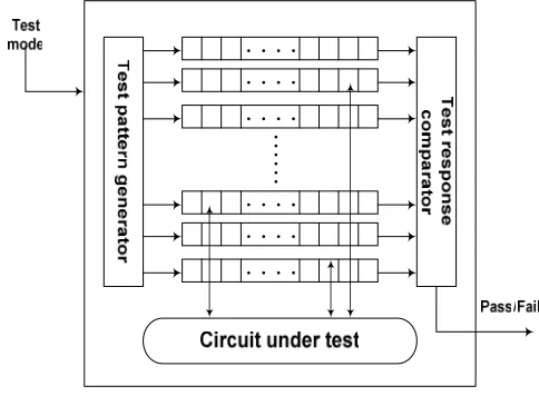
The basic components of BIST scheme are shown in fig.1. In a typical BIST environment, a TPG5 injects a number of test patterns into the scan chains which apply the pattern to CUT6 and the circuit response is captured back into the scan chains and compacted then compared to fault free signature in TRC7.
Usually LFSR8s are used as TPG or TRC, but some other kinds of TPGs are CA9 and circular self test path. In [4] TPG schemes have been divided into two categories: 1- Pseudo random testing and weighted random testing, in which, the test pattern can be generated using LFSR, CA, or circular self test path.
[image:1.595.319.561.453.631.2]2- Pseudo deterministic testing, in which, a LFSR or CA is synthesized such that a set of some pre computed tests are embedded into pseudo random test sequences of the LFSR or CA.
Fig. 1. A scan based BIST environment
In [5] some optimized LFSRs are introduced which does not have overhead.
3. High level testable synthesis
In high level synthesis of a circuit, behavioral description of system with a set of constraints such as time and area are given to synthesis tool as input to convert the behavior of a circuit to a set of operation elements, memory elements and interconnection elements. The task of the synthesis tool is to do resource allocation and scheduling on data path graph.
Exploiting self testability methods in a circuit has two major overheads: area and test time. Area minimization approaches usually maximize the sharing of test registers resulting in a fewer number of registers being modified for BIST without sacrificing test time (as our approach does) and time minimization approaches usually maximize the sharing of test registers resulting in fewer test sessions with maximum test concurrency, and may have drawback of large area overhead.
3.1. Scheduling
In this stage of synthesis, beginning cycle of each operation is determined and each operation is assigned to one or more cycles. Thus, after scheduling has done, the beginning time of execution of each vertex in data path graph is determined. Scheduling operations to occur in the same clock cycle requires more logic units, but spreading out the work over more clock cycles takes more time. Some times the an operation such as Iis not tightly forced to begin execution in a particular cycle and so I.earliest denotes the earliest cycle time and I.latest denotes the latest cycle time in which, the operation I, can start its execution.
There exist many scheduling algorithms. Two of theme is ALAP10 and ASAP11 which schedule an operation to
O.latest and O.earliest correspondingly.
In a SDFG12 the first cycle time in which, a variable
defined is called the birth time and the last cycle time in which, the value of a variable used is called death time of that variable. The time interval [birth, death] of a variable is called life time of it. Two variables are compatible, if their life times do not overlap. It means that they can share a register together.
3.2. Resource allocation
In this stage of synthesis, modules are assigned to perform operations, registers to store variables and interconnections (mostly MUXs) to interconnect the components to each other. The scheduling step assigns a particular clock cycle (relative to the start of the computation) to each operation that needs to be performed. Module assignment assigns functional units (such as adders) to particular steps in the schedule. We would like to schedule the operations so that the computation finishes in as few cycles as possible. Scheduling and resource allocation can be performed in any order, but in this paper we assumed that, scheduling has performed before resource allocation. We would also like to use as few functional units as possible. There are many algorithms to
10 As late as possible 11 As soon as possible 12 Scheduled data flow graph
perform resource allocation but most of them use one of compatibility or conflict graph. In both compatibility and conflict graphs, each vertex corresponds to a variable. If two variables are compatible, then the corresponding vertices in compatibility graph would be adjacent otherwise the corresponding vertices in conflict graph would be adjacent. Clearly these two types of register allocation graphs are complement of each other. Register allocation problem using compatibility graph can be solved by clique partitioning algorithm and register allocation problem using conflict graph can be solved by graph coloring algorithm.
For example assuming scheduled SDFG shown in fig.2, corresponding compatibility and conflict graphs are shown in fig.3.
1 *
2 * 2
+
1
+
LEA algorithm originally proposed for channel routing algorithm [7] is classified as a greedy algorithm and can be used to find the minimum number of registers needed for register allocation of a scheduled DFG. Given a SDFG to this algorithm, it makes a table of variables sorted by their life times then considering the life time of the variables, it greedily maps them to the registers which their mapped variables have not life time overlap with new one. For example assuming DFG shown in fig.2, Minimum 3 registers are needed.
3.3. Testability goals
3.3.1. Controllability and Observability Improvement Input registers are directly controllable and output registers are directly observable. Therefor for improvement of controllability (and observability) of internal variables, one can share a register between an internal variable and an input (output) variable.
If a register does not assign directly to an input or output, it may be controllable and observable through other registers.
3.3.2. Avoiding deep sequential depth and loops
After scheduling and resource allocation are done, DPCG13 can be derived from the architecture in which each node represents a register and each edge represents
R2
R3 R1
M1 M2
0 1 0 1
0 1
0 1 0 1
R1 R2 R3
M1 M2
0 1
0 1 0 1
4.b. Resource allocation without testability consideration
4.a. Resource allocation with testability consideration
Fig.4. Two resource allocations for example SDFG .
the largest combinatorial unit between two endpoint registers. The shortest path between two registers is called sequential depth between them. Sequential depth linearly affects the test cost [9].
When the source and destination of a sequential path is the same and its length is more than one and none of the registers in the path is I/O register, the path is called sequential loop and affects on test cost exponentially [10].
3.3.3 Self loop Avoidance
When the source and destination of a sequential path is the same and its length is exactly one, the register is called self adjacent and it means that register drives one of the inputs of combinatorial element of the path and receives its output.
During the synthesis process, creation of self adjacent registers must be avoided because in BIST methodology, normally a non-self adjacent register must be converted to BILBO14 which can support several modes of operations
14 Built in logic block observer
such as TPG, MISR15 as TRC, serial scan I/O and Normal
but it can not operate as TPG and TRC in the same time. A self adjacent register in BIST methodology must act as TPG and TRC in the same time [11]. BILBO can not operate as TPG and TRC simultaneously. So probably it would be converted to CBILBO16 which has more area and
time overhead than BILBO. The term “probably” is claimed because if there exist a distinct register for the output of a module and separate from its inputs, which can receive the output of that module, self adjacency of its input registers does not necessarily lead to use of CBILBO. Fig.4 illustrates two resource allocations for the DFG introduced in fig.2.
Fig.4.b has been synthesized for Area without self testability parameters consideration. Therefore, R1 and R3 registers should be modified as CBILBO and R2 to TPG for self testability. But in fig.4.a in which testability parameters were considered during the synthesis process,
R3 can receive the output of both modules, thus R1 and R2 can act as TPG and R3 as TRC with no need to CBILBO register. But number of MUXs in fig4.a is more than fig4.b.
So in module assignment, if having distinct output register for a module, separate of its inputs is considered, CBILBO overhead in the BIST scheme will be reduced when there is no way from self adjacency.
The minimum interconnects needed to model a circuit is achieved with Double clique algorithm [12].
3.3.4. Tradeoff
We try to improve all testability metrics with minimum overhead and penalty but some of these metrics are opposite to each other and a tradeoff must be established on achieving them. For example although sharing a register between an internal variable near output stages of DFG and an input register improves controllability of that internal variable but it may cause sequential loops in data path(s).
4. Proposed algorithm
For register allocation problem, a new flexible methods based on extended compatibility graph is presented. Our proposed method is about to satisfy testability parameters without violating structural constraints. Testability constraints are not as rigid as structural constraints, but violating those causes a circuit with low testability features. The Extended compatibility graph is a weighted compatibility graph in which, all edges are weighted. Weight of each edge in our extended compatibility graph is calculated by (1).
(1)
desire cycle
L con ob self threshold IJ
e W W W W Depth W
W = + + 2 +
In (1)
W
threshold is a constant which the value of it should select such that ifW
desire=
0
then>
0
IJ
e
W
. Simplythreshold
W
should be selected such that in every situation, the weights of all the edges would be positive.self
W
: If sharing a register between two variables, leads to a self adjacent register, then the connecting edge of those variables would have a positive value ofW
self, otherwise zero.ob
W
: If sharing a register between two variables, causes improvement in observability of each of them, then the connecting edge of those variables would have a positive value ofW
ob, otherwise zero.Since all output variables all directly observable, all edges between those variables and their compatible internal variables have weight of
W
ob>
0
.con
W
: If sharing a register between two variables, causes improvement in observability of each of them, then the connecting edge of those variables would have a positive value ofW
con, otherwise zero.Since all output variables all directly observable, all edges between those variables and their compatible internal variables have weight of
W
con>
0
.cycle
L
: If sharing a register between two variables, causes a sequential loop with maximum length ofL
cycle in DPCG, then the connecting edge of those variables would have a positive value ofL
cycle, otherwise zero.Depth: If sharing a register between two variables, causes
increasing in sequentialdepth
0
>
=
Depth
oldDepth
newDepth
then the value ofDepth in connecting edge of those variables would be a positive value, otherwise zero.
desire
W
: May be there are some other parameters which the designer considers to his/her own design that we did not considered to, such as power consumption or other metrics. He/she can affect register allocation by his/her parameters withW
desire. But an important notice is He/she should take care to selectW
desiresuch that the weight of the edges remain positive in every case.In selecting the weight of edges, related ratio of parameters is more important than the scalar value of them. For example if all testability metrics have the same importance for a designer, if one assigns the value of 1 to all
self
W
,W
ob,W
con,L
cycle, Depth ,W
desire parameters, the affect ofL
cycle would be two times of the ethers, because it exponentially contributes in our equation as the real effect ofL
cycle. So for this case with this rage of value assignment, one can assign all other parameters the value of 2 and 1 to theL
cycle . Obviously this kind of parameter assignment makes the exponential contribution ofL
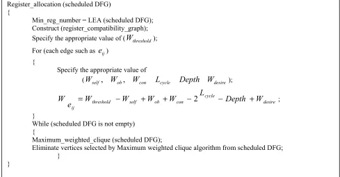
cycle ineffective.Our proposed algorithm is shown in fig.5. We used MWC17 algorithm to find maximum weighted clique [13, 14 and 15].
MWC is an algorithm to extract one maximum weighted clique from a given non-directed graph, by extracting all maximum cliques of it and comparing their total weights. Our insistence on remaining the weights of the edges positive is due to this fact that a MWC algorithm which can perform correctly with negative weights, has a very great time complexity, so its synthesis time overhead is considerable.
5. Experimental results
We assumed
W
self has the value of 5 and all other parameters had the value of zero. It means that just self testability is considered andW
self and2
Lcyclehave
non-zero value which
L
cycle is less effective in our register allocation contribution to minimize BIST area overhead.We have generated minimal area BIST solution for several high-level synthesis benchmarks. Here, we presented the results on the data path BIST synthesis. We choose 4 well-known academic high-level synthesis benchmarks: the 2nd order differential equation DiffEq [16], the auto regression filter element AR_Filter [17], the 5th order elliptic wave filter EW_filter [18] and the 8-point FIR filter FIR_filter [19].
In Table 1, we report the results obtained for data path BIST synthesis. For each synthesized benchmark data path, we report the number of registers, including the number of CBILBOs, BILBOs, TPGs, TRCs, and the number of multiplexers, and the extra area overhead due to the configuration for the BIST scheme. The BIST area overhead is expressed as a percentage increase in the gate count as a result of the modification for embedded BIST scheme. For the purpose of comparison, Table 2 shows traditional high-level synthesis results on the same
benchmarks without any BIST consideration achieved by LEA algorithm. It shows that considering requirements of the BIST scheme during behavioral synthesis, results in better BIST solution (less area overhead) can be obtained when compared to only structural DFT at low level. 6. Conclusions
In this paper, we exploited data path testability enhancement in high-level synthesis, and presented a technique to exploit test resource sharing to minimize the area overhead due to modification in behavioral synthesis domain. Study shows that not all of self-adjacent registers need to be modified to be CBILBOs. A sufficient condition was given. Testability constraints have been adopted to guide high-level synthesis process that has resulted in a minimal area test solution.
[image:5.595.52.541.288.543.2]Experimental results on some academic benchmarks demonstrate the effectiveness of the proposed approach to generate self-testable data path with low area overhead.
Fig.5. Proposed algorithm for testable register allocation
The most important advantage of our proposed technique is
W
desire, which allows the designer to apply the parameters which we did not consider, to the synthesis of the circuit. Fortunately for future advances in VLSI and VLSI testing, which may represent some new testingparameters, our technique is flexible enough to adapt with these new advances too.
Although we used this technique for register allocation, its application does not limit to this, for example our technique can be used for module allocation too.
Table 1- our experimental results
Multiplexers Registers
Modules BIST
overhead 6:1
5:1 4:1 3:1 2:1 TRC TPG
BILBO CBILBO
* -+
circuits
18.67% 0
0 0 3 9 2 3
1 0
4 1 1 DiffEq
7.11% 0
3 3 5 14 2
5 3
0 8
0 4 AR_filter
6.95% 1
1 7 6 5 3 5
0 1
3 0 5 EW_filter
27.38% 0
2 0 2 7 1 4
2 1
4 0 4 FIR_filter
Register_allocation (scheduled DFG) {
Min_reg_number = LEA (scheduled DFG); Construct (register_compatibility_graph);
Specify the appropriate value of (
W
threshold); For (each edge such ase
ij){
Specify the appropriate value of
(
W
self,
W
ob,
W
conL
cycleDepth
W
desire );desire cycle
con ob
self threshold
ij
W
Depth
L
W
W
W
W
e
W
=
+
+
2
+
;}
While (scheduled DFG is not empty) {
Maximum_weighted_clique (scheduled DFG);
Eliminate vertices selected by Maximum weighted clique algorithm from scheduled DFG; }
[image:5.595.66.534.658.735.2]Table 2- Expermental results of traditional method (LEA)
Multiplexers Registers
Modules BIST
overhead 6:1
5:1 4:1 3:1 2:1 TRC TPG
BILBO CBILBO
* -+
circuits
29.25% 0
0 0 4 6 1 2
1 1
4 1 1 DiffEq
17.66% 3
0 2 2 11 1
8 7
0 8
0 4 AR_filter
16.28% 1
2 2 3 8 2 5
0 2
3 0 5 EW_filter
46.06% 0
1 0 1 6 0 1
4 2
4 0 4 FIR_filter
References
[1] S. Tosun, O. Ozturk, N. Mansouri, E. Arvas, M. Kandemir, Y. Xie, W.-L. Hung, "An ILP formulation for reliability oriented high-level synthesis", Proceedings of the Sixth International Symposium on Quality Electronic Design (ISQED), March 2005, pp. 364-369.
[2] N. H. E. Weste, D. Harris ,CMOS VLSI Design A circuits and systems perspective, Addison Wesley, 2005
[3] K. Wagner and S.Dey, “High-Level Synthesis for Testability: A Survey and Perspective”, Proc. of ACM 1996 Design Auto. Conf. (DAC’96), p.131-136
[4] V. N. Yarmolik and I.V.Kachan, Self-Testing VLSI Design, Elsevier, ©1993
[5] D. k. Pradhan, C. Liu, K. chkraborty, "EBIST: A novel Test Generator with Built-In fault Detection capability", IEEE Tranc. On cad, volume 24(8), August 2005.
[6] L.B. Michael, D.A. Vishwani, Essentials of Electronic Testing for Digital, Memory and Mixed-Signal VLSI Circuits, Kluwer Academic Publishers, Dordrecht, 2000. [7] A. Hashimoto, J. Stevens, Wire routing by channel
assignment within large apertures, in: Proceedings of the Design Automation Workshop, 1971, pp. 155-169. [8] F.J. Kurdahi, A.C. Parker, REAL: a program for register
allocation, in: Proceedings of the Design Automation Conference, June 1987, pp. 210-215.
[9] M.L. Flottes, R. Pires, B. Rouzeyre, L. Volpe, Scanning data paths: a fast and effective partial scan technique, in: Proceedings of the DATE, Paris, February 1998, pp. 158-165. [10] M. Tien, C. Lee, High Level Test Synthesis of Digital VLSI
Circuits, Artech House Press, 1997.
[11] A. Steininger, Testing and built-in self-test--a survey, J. Syst. Archit. 46 (2000) 721-747.
[12] B.M.Pangrle, “On the Complexity of Connectivity Binding”, IEEE Trans. on CAD, Vol.10, pp.1460-1465, 1991. [13] D. Bahadur K. C, E. Tomita, J. Suzuki and T. Akutsu:
"Protein side-chain packing problem: A maximum edge-weight clique algorithmic approach," Journal of
Bioinformatics and Computational Biology, Vol.3, pp. 103-126, 2005.
[14] J.B. Brown, D. Bahadur K. C, E. Tomita, and T. Akutsu: "Multiple metods for protein side chain packing using maximum weight cliques," Genome Informatics, Vol.17, pp.3-12, 2006.
[15] Suzuki, J., Tomita, E. and Seki: "An algorithm for finding a maximum Clique with maximum edge-weight and computational experiments", The Information Processing Society of Japan, 2004.
[16] P.Paulin and J.Knight, “Force-Directed Scheduling for the Behavioral Synthesis of ASICs”, IEEE Trans. on CAD. Vol.8, No.6, 1989, pp.661-679
[17] S.Y.Kung, H.J.Whitehouse and T. Kailath, VLSI and Modern Signal Processing, Prentice-Hall, 1985
[18] N.Park and A.C.Parker, “SEHWA: A program for Synthesis of Pipelines”, Proc. of ACM/IEEE Design Auto. Conf. 1986, pp.454-460