Design of one-dimensional photonic crystals using combination
of band diagram and photonic gap map approaches
V. A. Tolmachev,1,2T. S. Perova,1,a兲J. Ruttle,1and E. V. Khokhlova1 1
Department of Electronic and Electrical Engineering, University of Dublin, Trinity College, Dublin 2, Ireland
2
Ioffe Physical-Technical Institute, Polytechnicheskaya 26, St. Petersburg 194021, Russia
共Received 16 May 2008; accepted 10 June 2008; published online 12 August 2008兲
The design of one-dimensional photonic crystals and the analysis of their optical properties have been performed using band diagram and forbidden gap map methods. It has been shown that the latter method is more useful for practical applications since共i兲it can be applied for any number of periods and共ii兲 it is more suitable for the selection of a filling fraction in a wide range of values using a single graphical presentation. Three different types of photonic crystals with small, medium, and high optical contrast were modeled using both methods. The features of the omnidirectional band gap formation for photonic crystals with small optical contrast and low number of periods have been explained. The formation of a one-dimensional photonic structure with limited number of periods and omnidirectional band gap close to that for an infinite periodic structure has been discussed. ©2008 American Institute of Physics.关DOI:10.1063/1.2963700兴
I. INTRODUCTION
Microphotonics has been recently recognized as one of the ways to further the development of communication and information technologies. Its hardware component base is rapidly growing. It is recognized that the most important points for the development of new technologies are function-ality, low cost, and accessibility. From these points of view, silicon is the most suitable material due to its low cost and well-developed complementary metal-oxide semiconductor processing.1 Silicon-based optoelectronics could provide a low-cost solution for high-speed interconnects for data cen-ters and other enterprises. The enabling technologies rely on fundamental building blocks such as silicon-based laser, am-plifier, and modulator.1,2 Recently new areas of research in microphotonics were opened up due to the elaboration of the theory and application of photonic crystals 共PCs兲. PCs pos-sess unique optical properties and can be used as reflectors, waveguides, attenuators of spontaneous atomic emission, de-vices for controlling emission in microcavities, and others.3–5 Furthermore, PCs have demonstrated their potential for ap-plication due to a number of microphotonic devices utilized recently.6During the last decade particular attention has been paid to the development of devices based on one-dimensional共1D兲PCs, thanks to certain advantages of these devices over two- and three-dimensional 共3D兲 PCs. These advantages are mainly related to their simpler fabrication, low cost, and the possibility of having simultaneous total reflection in a certain frequency 共or wavelength兲 range for light at any incident angleand polarization, i.e., to possess omnidirectional bands共ODBs兲.7–9
The design of a 1D PC normally starts with the selection of the wavelengthof its operation. Then, the materials with corresponding refractive indices,n1 andn2, for suitable
pe-riodic structure fabrication are chosen. Based on the above selection, the geometric thickness of both components, d1 and d2, will be determined in accordance with the Bragg condition
/2 =n1d1 +n2d2, 共1兲
wherendis the optical thickness of the corresponding com-ponent.
For equal optical thicknesses of each component nd =/4, the maximum width of the stop band is achieved for the required wavelength . Several approaches can be used in order to determine the optical properties of a 1D PC. One of these is to calculate the band diagrams共BDs兲 共Ref.10兲for the selected filling fractions f=d1/共d1 +d2兲, where d1 +d2 =⌳ is the lattice constant of the PC. The second approach based on the gap map 共GM兲 presentation of photonic band gaps 共PBGs兲was described in Ref.5. For drawing the GM, in principle, both the BD 共Ref.8兲and the reflection spectra method11can be used. The calculation of the reflection spec-tra of 1D PCs with a certain number of lattice periods,m, is normally performed using the transfer-matrix method
共TMM兲.12It was shown previously that the GM approach is very useful in the selection of ODB structures,8,13as well as tunable11and composite14photonic structures since it allows quick and easy analysis of structures for a large set of spectra
共normally around 100兲to be done practically on one plot. In this paper we apply the GM approach based on both the aforementioned methods for the design and analysis of optical properties of 1D PCs. First, we used BD calculations for periodic structures with an infinite number of periods and for one predicted filling fraction. By doing this we were able to determine the position and width of the PBGs including ODB. Following this, the GM method was applied, which enabled us to select the proper filling fraction in a large range of possible numbers of mand incidence angles. The advan-tage of the GM approach is that the design of ODB from the
a兲Author to whom correspondence should be addressed: Tel.: ⫹3531
8961432. FAX:⫹3531 6772442. Electronic mail: perovat@tcd.ie.
point of view of technical realization, including minimiza-tion of the number of periods m, is possible. Finally, in the selected wavelength range of ODB and using the obtained optimal filling fraction, the reflection spectra can be ana-lyzed. With this final procedure we can obtain information about the features of the reflection spectra, namely, the maxi-mum value ofR, the spectra linewidth, the sharpness of the stop band edges, the presence of interference fringes between stop bands, and others. The approach suggested is demon-strated, by way of example, on the 1D PC, divided relatively into high, medium, and small refractive index contrast struc-tures.
II. BAND DIAGRAM METHOD
To create BDs the Bloch solution was used in the same way as described in Ref. 10. Consider a 1D PC with an infinite number of layers. This means that a translational symmetry along the periodic direction will lead to a Bloch solution of the field component
cosK⌳= cos共k1xd1兲cos共k2xd2兲
−Msin共k1xd1兲sin共k2xd2兲, 共2兲
whereKis the Bloch wave vector and k1xandk2xare thex components of the wave vectors k1 andk2 of the first and second constituent layers, respectively. The parameter M is dependent on the polarization transverse-electric 共TE兲 and transverse-magnetic共TM兲accordingly,
M⬅
冦
1 2
冉
k2x k1x
+k1x k2x
冊
, TE
1 2
冉
n12k2x n22k1x
+n2 2
k1x n12k2x
冊
TM.
冧
共3兲
The PBG exists in the range of frequencies共wave numbers兲 where the solution has a nonzero imaginary part. These fre-quencies are calculated and plotted versus the angle of inci-dence from the external medium onto the first layer. The external medium has a refractive index of 1. This results in a graph similar to Fig. 1共x兲, where the normalized frequency
共NF兲is 2c/⌳=⌳/.
III. THE GAP MAP APPROACH
To create a GM, one must first calculate the reflection spectrum of the PC structure. This is achieved by calculating
the optical response of PCs using TMM 共Ref. 12兲. The 2
⫻2 complex matrix S describes light propagation through the PC
S=关共IL兲1共IL兲2兴m, 共4兲
whereIis the matrix that describes the interface between the two subscripted media, L is the matrix that describes the subscripted media, andmis the number of periods.I andL are based on the refractive indexnof the materials, the thick-nessd of the materials, and the incident angle at which the light strikes the surface and its polarization.
Once the refractive index, incident angle, lattice con-stant, and the number of periods are chosen, the reflection spectrum of the structure is calculated using Eqs.共4兲and共5兲
for a range of filling fractions from 0.01 to 0.99,
R=兩关S1,0/S0,0兴2兩. 共5兲
For each of the reflection spectra, the region where the re-flection was greater than 0.999 was recorded on the graph. Thus, the obtained PBG ranges were then plotted, together with all the other filling fractions, to give a graph called GM. The end result is displayed in Fig. 2共a兲as an example. The graph gives a number of PBGs where the reflection is greater than 0.999 as a general rule, unless stated otherwise for some specific cases.
IV. PHOTONIC CRYSTALS WITH HIGH OPTICAL CONTRAST
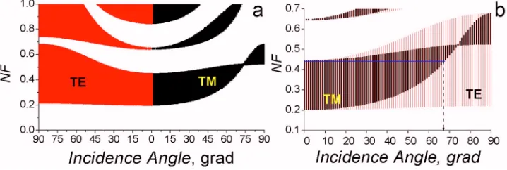
In this case we consider a photonic structure with a high optical contrast of n1/n2 = 3.42/1 and optimum filling frac-tion for the second component at 0.774 from formula 共1兲. The refractive index of the media for incoming and outgoing light beams is 1. For BDs shown in Fig. 1共a兲, the blueshift
共to higher normalized frequencies兲 with increasing angle of incidence of PBGs for both polarizations is seen. The overlap of the lowest PBGs for the same condition is shown in Fig.
1共b兲. From the latter figure we can deduce that ODB in such PC cannot exist due to the fact that the short wavelength edge of the TM range for angles greater than 67° does not have a mutual overlapping range with PBGs with normal incidence of light.
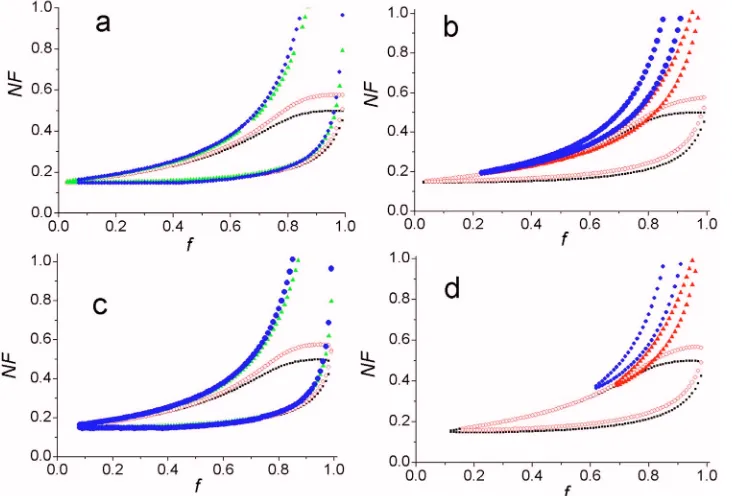
In order to investigate what the GM method reveals, GMs are calculated over a number of incident angles in the range of 0°–85° and for periods of 20 and 100 for both TE and TM polarizations 共Fig.2兲. From the GMs of TE polar-ization, as shown in Fig.2, it can be seen that the regions of PBG are expanding with some blueshift to higher normalized
[image:2.612.51.410.52.173.2]frequencies, as seen from the BD in Fig. 1. For the PBG regions of TM polarization the opposite is observed, namely, shrinkage of the PBG region with increasing angle of inci-dence. It can be seen in Figs. 2共b兲 and 2共d兲 that the PBG region with TM polarization and angle of incidence from 67° to 85° does not overlap with the PBG obtained for angle 0°. Therefore, for structures with high optical contrast, ODB cannot be obtained at any f value.
V. PHOTONIC CRYSTAL WITH MEDIUM OPTICAL CONTRAST
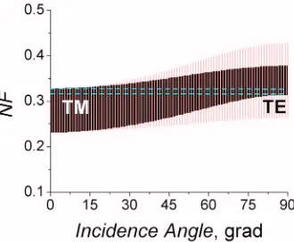
As was already demonstrated in Fig.1共b兲, ODB is de-fined by the range of overlapping of PBGs calculated for 0° and maximal possible angles of incidence for TM and TE modes. The BDs for the photonic structure of medium opti-cal contrast n1/n2 = 1.5/3.42 with the optimum filling frac-tion of the first component at 0.695 are demonstrated in Fig.
3. In this case, the overlapping of the PBGs for TM and TE polarizations reveals an ODB. With a range of NF of 0.23– 0.3 this gives an ODB width⌬NF of 0.07. Since the TE is wider than the TM mode, the region of ODB is in fact form-ing from the width of the TM mode in the incident angle range from 0° to 85°, as demonstrated in Figs. 1 and 3. Therefore, Figs.4共a兲and4共b兲 show only these two regions
共0° and 85°兲for TM mode. The overlapping regions demon-strate large ODB areas for PC withm= 20 andm= 10.
To learn how the number of periods influences the for-mation of an ODB region, the corresponding dependences of
⌬NF versus filling fraction f were plotted using the data obtained from GM and BD calculations 共see Fig. 5兲. From these graphs one can see that the parameters of the ideal PC
共with infinite number of periods兲are practically the same for PCs with 40 and more periods. Therefore, the PC structure possessing the ODB is totally formed atm= 40. Although the PC with ODB can also be formed at m⬍40, the range of permissible f values is narrowing along with the width of
ODB. It can also be seen that a quite substantial ODB region is observed for PC with six periods, and this is important from the point of view of m minimization. In this case the range of permissible f values with enough ODB is very small.
Figure5 shows that a PC with⌬NF= 0.03– 0.07 can be formed from a photonic structure with a number of periods m⬎20 andf varying in the range of 0.4 to 0.85. Therefore, the design of medium contrast PC with omniband can be performed in a significantly wide range of spectra using a range of⌬NF, number of periods, and filling fractions.
VI. PC WITH SMALL OPTICAL CONTRAST
[image:3.612.50.416.51.299.2]The BDs of photonic structure with small optical con-trast n1/n2 = 1.42/2.4 and optimum filling fraction of the first component taken as 0.628 are demonstrated in Fig. 6. The overlapping of TM and TE PBGs shows that for both polarizations and any incident angle, there is a PBG in the range of NF= 0.32– 0.33. Comparing this with a PC with medium contrast, the ODB region reduced down to ⌬NF = 0.01. GMs for a number of incident angles with a range of
FIG. 3. 共Color online兲BD for TE and TM polarizations of a 1D PC with medium optical contrastn1/n2 = 1.5/3.42 and the filling fraction of the first componentf1= 0.695 overlapped with the ODB indicated by dashed lines.
[image:3.612.352.518.592.718.2]0°–85° and for a number of different lattice periods varying from 10 to 100 for TE and TM polarizations were calculated. Figure 7 shows GMs form= 10 andm= 20. The same ten-dency for ODB shrinkage is seen when the number of peri-ods decreases关Figs.7共a兲–7共c兲兴. It is worth noting that for PC withm= 10, the PBG behaves slightly different with the TM PBG regions shrinking between 0° and 44°, disappearing between 45° and 82°, and reappearing and expanding from 83° to 85°. This feature is presented in Fig. 7共d兲 in more detail with an increased number of incident angles. These characteristics are not observed for the TE mode 关see Fig.
7共c兲, PBG region for 60°兴.
In order to clarify this feature, the reflection spectra for TM polarization are demonstrated form= 10 and filling frac-tion f1= 0.628. These reflection spectra for f= 0.628 are pre-sented in Fig.8共a兲for different incident angles, including the range of angles where the PBG regions disappear. One can see that the PBG has a blueshift, as predicted, as the incident angle increases from 0° to 85°. More details can be seen by looking at the reflection range from 0.99 to 1. This shows that as the incident angle increases, the maximum reflection decreases below the selected criteria of 0.999 for the GM calculated in the range of angles from 45° to 82°关Fig.8共b兲兴. It can also be seen from the reflection spectra shown in Fig.
8 that the width of the PBG is also dependent on the selec-tion of the cutoff reflecselec-tion value. For example, if a cutoff reflection value of 0.995 was chosen, then the PBG within a small range of normalized frequencies will appear in all angles of incidence on the GM plot.
The next step is to determine the ODB by using the GM method. In order to do this, GMs with different incident
angles and polarizations must be overlapped. Since the PC with the number of periodsm= 10 is not good at reaching the reflection cutoff of 0.999 for certain incident angles共as men-tioned above兲, we shall consider PCs with periods ranging from 15 to 100. It can be seen that an ODB for a PC with the number of periods m= 20 can appear for a range of filling fractions from 0.44 to 0.7 关Fig. 7共b兲兴. The width ⌬NF can now be determined for a range of filling fractions and period numbers. These data were then placed on a graph in Fig.9共a兲
to compare with the results obtained from the BD. The cal-culated curve for the PC with infinite number of periods is located lower than the one for the PC withm= 100. This can be explained by the fact that the calculations for the first PC were carried out at R= 1, while for the second PC we used the cutoff value ofR= 0.999. This resulted in the PBG for the second PC being slightly wider than the first PC. Similar to the previous case for PC with medium contrast, the analysis using the GM共or the set of reflection spectra for differentm values兲 gives the possibility to estimate the degree of ODB formation for a PC structure with properties close to the in-finite PC in width⌬NF= 0.005– 0.015. As can be seen in Fig.
9共a兲, this is a PC with number of periods m⬎40 and f = 0.4– 0.7. Thus, the formation of structures for the small contrast PC with ODB is starting atm= 15 and completed at m= 40.
It should be noted that the maximum position for the dependences ⌬NF vs f, as shown in Figs.5 and 9共a兲, does not correspond to the optimal f value determined for the quota wavelength thickness and is shifted to the larger f
[image:4.612.52.408.50.195.2]angles for TM polarization with the number of periods 共a兲20 and共b兲10. Shaded regions correspond to ODB.
[image:4.612.354.519.583.719.2]FIG. 5.共Color online兲PC with medium optical contrast. Width of the ODB vs the filling fraction obtained for a number of periods using the GM method and for an infinite number of periods using the BD method.
[image:4.612.90.259.599.717.2]FIG. 7. 共Color online兲 GMs for TM and TE polarizations showing the low-est PBG of a 1D PC with small optical contrast with a range of angles of in-cidences overlapped: 共a兲 and 共b兲 for
m= 20 and共c兲and共d兲form= 10.
[image:5.612.52.430.42.764.2]FIG. 8.共Color online兲The TM reflec-tion spectra of the PBG for 1D PC with small contrast calculated at dif-ferent angles共indicated by numbers in grads兲of incident light with the num-ber of periodsm= 10 and filling frac-tionf= 0.628.共a兲Reflection spectra at different angles of incidence.共b兲The spectra of PBG for the range of reflec-tion from 0.99 to 1. The vertical lines show the level共criteria兲of reflection at 0.999共gray line兲and at 0.995共black dashed line兲 for the selection of the PBG’s edges used for the drawing of the PBG’s regions on the GM.
taken into account during the design of PCs with ODB. The intersection of this set of graphs关Fig.9共a兲兴with line at f= 0.6 demonstrates the dependence of⌬NF on the num-ber of lattice periods关Fig.9共b兲, curve 2兴. From this depen-dence it can be seen that as the number of periods increases,
⌬NF also increases, as well as the formation of the structure with⌬NF parameters close to PC, determined from BD, and being completed for m⬎40. In a similar manner it can be concluded that there is complete formation of the medium-contrast PC structure with ODB afterm= 20共forf= 0.7兲 关see Fig.9共b兲, curve 1兴.
As mentioned above, the possibility of design and opti-mization of 1D PCs using GMs was demonstrated in Ref.8. The distinction with our approach is that we are using the TMM for the calculation of the reflection spectra, based on which the PBG共and then GM兲can be drawn. This enables us to design 1D PCs with finite number of lattice periods. Thus, using our approach in the course of optimization of the struc-ture, another important parameter, namely, the number of lattice periodsm, is included. Decreasing the number of pe-riods can lead to a significant decrease in the PBG/ODB width, and therefore a reduction in the number of possibili-ties for the selection of the filling fraction.
Recently, another approach using reflection spectra cal-culations and their presentation on one 3D plot has been suggested in Ref.15for the design of PCs. From our point of view such presentation looks bulky and complicates the se-lection of the optimal PBG range. We believe that the GM presentation for optimization of ODB for 1D PC is more visual and clearer compared with the large set of spectra presented on a 3D plot.
VII. CONCLUSIONS
In summary, it has been demonstrated that it is possible to model PCs using both the BD and the forbidden GM methods. From these methods we are able to discern whether an ODB is possible and what range of operation it would
formed from photonic structures of medium optical contrast with a number of periods, starting fromm= 6 andf varying in the range from 0.4 to 0.85. A quite interesting behavior of PBGs has been observed on the GM for small contrast PCs withm= 10. In particular, the disappearance of PBGs in TM polarization at certain angles of incidence was revealed. This effect was explained by the small decrease in the reflection coefficient in the PBG region. The formation of 1D photonic structures with an ODB gap close to an infinite periodic structure has been discussed.
ACKNOWLEDGMENTS
This work was supported by the Science Foundation Ire-land共SFI兲and Program RAS “Laser materials based on ac-tive media and optics of structured materials.”
1A. Liu and M. Paniccia, Physica E共Amsterdam兲35, 223共2006兲. 2R. Soref,IEEE J. Sel. Top. Quantum Electron.12, 1678共2006兲. 3E. Yablonovitch,Phys. Rev. Lett.58, 2059共1987兲.
4S. John,Phys. Rev. Lett.58, 2486共1987兲.
5J. D. Joannopoulos, R. D. Meade, and R. D. Winn, Photonic Crystals 共Princeton University Press, Princeton, NJ, 1995兲.
6Photonic Crystals. Advances in Design, Fabrication, and
Characteriza-tion, edited by K. Busch, S. Lölkes, R. Wehrspohn, and H. Föll共 Wiley-VCH, Weinheim, 2004兲.
7Y. Fink, J. N. Winn, F. Shanhui, C. Chiping, J. Michel, J. D. Joannopoulos,
and E. L. Thomas,Science282, 1679共1998兲.
8D. N. Chigrin, A. V. Lavrinenko, D. A. Yarotsky, and S. V. Gaponenko,
Appl. Phys. A: Mater. Sci. Process.68, 25共1999兲.
9P. St. J. Russell, S. Tredwell, and P. J. Roberts,Opt. Commun.160, 66 共1999兲.
10P. Yeh,Optical Waves in Layered Media共Wiley, New York, 1988兲. 11R. M. A. Azzam and N. M. Bashara, Ellipsometry and Polarized Light
共North-Holland, Amsterdam, 1977兲.
12V. A. Tolmachev, T. S. Perova, and K. Berwick, Appl. Opt. 42, 5679 共2003兲.
13V. A. Tolmachev, T. S. Perova, and R. A. Moore,Opt. Express13, 8433 共2005兲.
14V. A. Tolmachev, T. S. Perova, and K. Berwick,J. Appl. Phys.99, 033507 共2006兲.