Electron Microscopy and Spectroscopy in the Analysis of
Friction and Wear Mechanisms
LUO, Quanshun <http://orcid.org/0000-0003-4102-2129>
Available from Sheffield Hallam University Research Archive (SHURA) at:
http://shura.shu.ac.uk/21748/
This document is the author deposited version. You are advised to consult the
publisher's version if you wish to cite from it.
Published version
LUO, Quanshun (2018). Electron Microscopy and Spectroscopy in the Analysis of
Friction and Wear Mechanisms. Lubricants, 6 (58), 1-19.
Copyright and re-use policy
See
http://shura.shu.ac.uk/information.html
lubricants
Review
Electron Microscopy and Spectroscopy in the
Analysis of Friction and Wear Mechanisms
Quanshun LuoID
Materials and Engineering Research Institute, Sheffield Hallam University, Howard Street, Sheffield S1 1WB, UK; q.luo@shu.ac.uk; Tel.: +44-114-2253649
Received: 30 May 2018; Accepted: 2 July 2018; Published: 4 July 2018
Abstract: Friction and wear take place on two solid surfaces in sliding contact as a result of the mechanical, thermal, and chemical interactions with the participation of environmental species. These interactions lead to the formation of a tribo-layer or tribofilm, which attaches on the worn surfaces, and consequently, contributes to the variation of the friction and wear behaviour. Electron microscopy and the associated spectroscopic analyses are powerful in probing these matters in spatial resolutions from micro to atomic scale. This article provides a review of the author’s work in the wear and friction mechanisms of physical vapour deposition (PVD) hard coatings, in which various scanning electron microscope (SEM)- and transmission electron microscope (TEM)-based microscopic and spectroscopic techniques were employed. Understanding on the failure mechanisms and the origin of self-adaptive friction has been improved to the nano-scale. Other related issues are also discussed, such as sample preparation techniques for cross-sectional electron microscopy, energy dispersive X-ray spectroscopy, and electron energy loss spectroscopy.
Keywords:electron microscopy; energy dispersive X-ray spectroscopy (EDX); electron energy loss spectroscopy (EELS); worn surface analysis; tribofilms
1. Introduction
Friction and wear are the most common phenomena in machinery and engineering practices. Wear, along with fracture and corrosion, forms the major failures of engineering materials. Therefore, great efforts have been made in the control of friction and wear, including research on wear resistant coatings [1–7], hand and lubricious coatings [8–10], and the understanding of the associated mechanisms of friction and wear [10–14]. For the latter, an improved understanding on the mechanisms has been attributed to the advances in laboratory techniques of materials analyses and characterization, especially the metallographic and spectroscopic techniques that are based on electron microscopy. This paper is a survey of the analytical electron microscopy techniques employed in the author’s studies of wear mechanisms [14–30].
Friction and wear occur on a solid surface when it contacts with and slides against another solid surface under pressure, in which various interactions occur. These interactions include the adhesive attraction and even cold welding, interlock between asperities and subsequent breaking, elastic and plastic deformation, conversion of shearing strain energy to frictional heating, and the resulted softening, as well as sliding and friction activated chemical reactions. These interactions result in wear and material transfer, along with the microstructural evolution and tribo-chemical changes of the worn surfaces. In some cases, a thin layer of powdered wear debris is attached on the worn surface to play a role of the third part in the sliding friction zone, which thereafter influences the friction coefficient. For example, the so-called self-adaptive lubricity can be attributed to the formation of a low-friction tribofilm [8,10,12–14,20–25]. On the other hand, a tribofilm may behave with high friction and consequently results in more pronounced wear [23,25,29]. In view of the wear property, tribofilms
have also been found to change the stress distribution on the wear contact zone and to be associated with the deformation of the top worn surface [15–20]. The friction behaviour of the tribofilms is related not only to the sliding materials themselves, but also to the participation of environmental species, such as oxygen and hydro-oxygen (water) [11,27,28].
In recent years, orthopaedical implants have attracted the research interests to understand the tribological performance and the associated mechanisms of wear and friction. Typical implant materials include CrCrMo alloys and ceramics, as well as the applications of physical vapour deposition (PVD) hard coatings [31–34]. It has been found that the surface conditions, such as the applied mechanical and electrochemical polishing as well as the adhesion property of hard coatings, have strong influence on the service life performance [35,36]. The mechanisms of the associated friction and wear are related to the generation of lubricious tribofilms [37–40]. To investigate the mechanisms of the surface material interactions, microscopic and spectroscopic techniques have long been employed as the major tool, including imaging and spectroscopic chemical analyses.
In view of imaging techniques in wear failure investigations, high-pixel camera and visual inspection are both widely applied, e.g., in assessing the wear modes at macro- and sub-millimetre scales. Optical microscopy (OM) is often employed to observe the wear phenomena of microstructure at micrometre scale [15,16]. Scanning electron microscopy (SEM), especially the high-resolution SEM equipped with field emission gun (FEG), can greatly increase the spatial resolution in microscopic observations as compared to OM. Owing to the high resolution, wear features can be observed down to sub-micron and nano-scales [21,24–26]. Another obvious advantage of SEM is its large depth of focus, which allows imaging of three-dimensional features on most worn surfaces and wear particles. Moreover, most SEM instruments have also been equipped with powerful capability of chemical analysis, e.g., energy dispersive X-ray (EDX) spectroscopic analysis, which enables simultaneous microscopic observation and chemical analysis of wear features [25–30]. Transmission electron microscope (TEM) is the most widely used instrument in comprehensive characterization of materials, with its advantages of the best spatial resolution in observing extremely small species and the capability in performing combined metallographic, crystallographic, and spectroscopic analyses [17–22]. In particular, TEM provides a powerful analytical tool in the characterization of nano-structured transition metal nitride coatings, such the multilayer TiAlN/VN coatings [41–45]. In addition, TEM based spectroscopic chemical analyses are superior to SEM-EDX in detecting light elements, including EDX and electron energy loss spectroscopy (EELS) [14,23,25,27,28,46–50]. Therefore, TEM has become a platform of several advanced nano/atomic scale characterizations. The application of TEM in wear mechanism study is also attributed to the development of cross-sectional sample preparation, which allows characterization of worn samples from the upmost worn surface to certain depths of subsurface regions.
In the following parts, this paper will introduce the application of the analytical electron microscopy techniques, as mentioned above, in the wear mechanism studies of various nano-structured hard coatings grown by physical vapour deposition (PVD). Details of the research can be found in previous publications [14–30]. In particular, it has been found that, the sliding wear of vanadium-containing transition metal nitride TiAlN/VN coatings led to the formation of a multi-component Ti–Al–V–N–O tribofilm on the worn surface. Such tribofilm exhibited varied friction coefficient highly dependent on the testing temperature and on the relative humidity. Such environment-dependent friction behaviour has also been found in carbon-containing nitride coating TiAlV(N,C)/a-C [28]. The characterization of wear debris and tribofilms has provided explanations to these phenomena. This paper will only focus on the methodology of the techniques, with a few examples to demonstrate the data interpretation.
2. Sample Materials and Tribological Tests
multicomponent coatings TiAlN, TiAlCrN, and TiAlCrYN, and nano-structured multilayer coatings TiAlN/CrN, TiAlN/VN, and TiAlCN/VCN [4,17,23,24,41,42]. The coatings were grown using an industrial-scale magnetron sputtering coating equipment, each under its own optimal deposition conditions. Detailed sputtering deposition condition, microstructure characterization, mechanical and tribological properties, and industrial applications can be found in previous publications [4,28,41–48]. In brief, these coatings were grown by unbalanced magnetron sputtering in vacuum with mixed gas flux of argon and nitrogen, properly controlled power input, and a suitable substrate bias voltage. Ion etching was applied prior to the coating deposition by means of either cathodic glow discharge or high-power impulse magnetron in order to strengthen the adhesion properties. The nano-structured multilayer coatings showed super hardness of 30–40 GPa and excellent tribological properties both in the in-house sliding wear tests and in machining industrial alloys, such as hardened steels (the TiAlN/CrN coating), aerospace Al-Si-Mg, and automotive eutectic Al-Si alloys (the TiAlN/VN and TiAlCN/VCN coatings).
A CSM-manufactured ball-on-disc tribometer (CSM Instruments, Peseux, Switzerland)) was employed in most of the tribotests [26–29]. The disc samples were the transition metal nitride coatings grown on pre-polished high speed steel coupons, which slid against a ball counterpart of either alumina ceramic or cemented WC carbide of 6 mm in diameter. The applied normal load and linear sliding speed were 5 N and 0.01 m·s−1, respectively, while the tests were carried out in different time under ambient conditions.
3. Analytical Scanning Electron Microscopy
SEM is the most widely used instrument in routine materials characterization for its advantages of flexibility in sample preparation, easy data interpretation, and multiple functions of imaging, chemical analysing, and the recently developed electron back scattered diffraction (EBSD). For dozens of years, SEM has been one of the essential tools in failure investigation, including comprehensive analyses of wear debris, worn samples, and subsurface microstructure. In SEM, an electron beam that is generated in the filament, which can be tungsten, LaB6ceramic, or a field emission gun, is focused to an extremely
small size to scan over a defined area of a sample surface. During the scanning, several signals are emitted as a result of the physical interactions between the electron beam and the sample volume in the small volume beneath the beam-focused area. These signals are simultaneously collected by various detectors either to form images or to perform spectroscopic analyses.
Secondary electron (SE) imaging is the most straightforward analysis of surface morphology. Because of the very low energy, secondary electrons that are generated in the interaction volume are mostly absorbed by the sample matrix, except those emitting from the extreme surface. Therefore, the spatial resolution of SE imaging is the best in all of the SEM image modes. Also, for this reason, the SE intensity depends strongly on the geometric orientation of the electron beam scanned surface, which makes it sensitive to the variation of surface morphology. Consequently, SEM images in SE mode provide a tool to observe the three-dimensional morphology of rough surfaces, such as worn surfaces, fractures, and chemically etched metallographic surfaces. SE imaging is the mostly used technique to observe wear products, including worn surfaces and wear debris [26,28].
Energy dispersive X-ray (EDX) spectroscopic analyses have become an essential attachment of most SEM instruments, which allow simultaneous chemical analysis during SE or BSE observation. Especially, recently developed software packages have enabled several modes of SEM-EDX analyses. When the incident electron beam is fixed at a point or is defined to scan within a special area or line, a spectrum can be obtained, from which the chemical compositions of the electron-hit point or area can be determined either qualitatively or quantitatively. Using the SEM-EDX spectroscopic analysis, it is convenient to analyse the overall chemical composition of a sample or the chemical compositions of various areas. In interpreting an EDX spectrum, one should bear in mind about the overlapping characteristic X-rays, such as the overlaps between N–K and Ti–L, O–K and Cr–O, as well as V–L. A few examples will be discussed later. If the analysis is paid more attention on one or more elements in an imaged area, the line-scan mode is operated by confining the scanning electron beam in a defined length, e.g., across a grain boundary or an object of interest, to get the relative (qualitative) profiles of the selected elements. Similarly, the scanning can be made in a pre-defined area, instead of a period of length, to obtain a two-dimensional relative distribution of the featured elements, which is known as element-mapping analysis [30].
SEM-EDX analyses provide reasonable accuracy to the analyses of heavy elements, e.g., most metals in the periodic table. However, its accuracy is greatly restricted in the analysis of light elements, i.e., from boron to oxygen in the periodic table. The characteristic X-rays of these light elements have very low energies, which makes them mostly absorbed by the sample matrix, except the X-rays emitting from the outmost surface. Consequently, the integrated intensities of these X-rays are much lower than the characteristic X-rays of heavier elements, because the latter emit both from the outmost surface and from certain depth (up to several micrometres). Although SEM-EDX is less sensitive in analysing light elements, nevertheless, it provides the feasibility to detect dissimilar matters, such as tribo-oxidation films or particles, as compared to the bulk worn surface. Another limitation of SEM-EDX is the scattering data in analysing carbon, which arises from the unavoidable presence of carbon contamination of samples.
Given these functions as described above, SE imaging is normally used to observe the morphology of worn surfaces and wear debris, from which the wear modes and wear mechanisms are determined. BSE imaging is applied to distinguish the regions of different chemical compositions on the worn surfaces analysed, such as the products of tribo-chemical wear and transferred matter from the counterpart. Then, SEM-EDX spectroscopy and related line scanning and two-dimensional (2-D) mapping provide more accurate analyses of the chemical compositions.
In addition, SEM can also be employed to characterise the microstructure changes in a depth of a worn surface [30,49]. This analysis is achieved by preparing a vertical cross-section of the worn surface. Consequently, the SE and BSE imaging can be applied to investigate wear induced changes in the microstructure, such as deformation, cracking, delamination, transferred layer and intermixing, and tribofilm formation. The experimental procedure of cross-sectional sample preparation will be described later.
4. Analytical Transmission Electron Microscopy
of resolving the atom stacking structure at extremely high magnification when it is operated in the so-called phase-contrast mode, i.e., high-resolution electron microscopy (HREM). HREM possesses the best spatial resolution in microscopic observations, which can be applied to make lattice imaging, e.g., the ordered atomic stacking, dislocations and stacking faults, and short-range ordered domains in amorphous and nanocrystalline samples [21,27,28].
TEM can perform chemical analyses in micro- and nano-scales by means of EDX and EELS. In TEM-EDX analysis, the characteristic X-rays that are emitted from the electron-sample interaction volume are collected by a detector positioned in close vicinity of the sample. Then, EDX spectroscopic analysis is performed in order to determine the chemical composition, whereas TEM-EDX is superior to SEM-EDX, in that it can analyse the composition of an area as small as only a few nanometres in diameter. Furthermore, the capability in analysing light elements is enhanced, owing to the elimination of mass absorption of the low-energy X-rays [22,23,29]. In advanced analytical TEM, the incident electron beam can be configured to scan over the sample, to achieve the functions of line-scan and elemental mapping.
EELS is another TEM based spectroscopic chemical analysis. The principles and applications of TEM-EELS can be read from literature [50–57]. Unlike TEM-EDX, which analyses the characteristic X-rays directed from the electron interaction volume, the principal of TEM-EELS analysis is based on the fact that the emission of a characteristic X-ray signal corresponding to a specific energy band of an element is accompanied by the same amount of energy loss in the transmission electron beam [14,47,49,50]. The electrons with the decreased energy form inelastic scattering. Then, a special prism lens is fitted to translate the transmission beam into a spectrum, in which the intensity of the electron beam is displayed as a function of the actual energy, or energy loss as compared to the energy of elastic scattered electron beam. EELS is superior to EDX in at least two aspects. Firstly, it totally overcomes the drawback of mass absorption in the EDX analysis of light elements, because the actual electron intensity reflects the transmission electron beam instead of the extremely weak signals of X-ray emission. Therefore, a distinct edge of energy loss can be obtained from every detected light element. Secondly, EELS analysis has more than ten times better energy resolution than EDX analysis, which allows the separation of the characteristic edges having very close energy levels. For example, the N–K and Ti–L edges can be easily separated in EELS analysis. Moreover, the extremely high energy resolution of EELS makes it possible to conduct a more precise analysis on the shape of a characteristic energy edge, for the edge shape is strongly influenced by the chemical environment of the analysed element. Such analysis is called energy loss near edge structure (ELNES). For example, TEM-EELS was applied to identify sliding induced transition of carbon from sp3 to sp2 bond [12] and to separate stoichiometric and sub-stoichiometric nitrides, as well as other chemical structures [52–57]. In addition to the functions of spectroscopic chemical analyses, TEM-EELS is also able to show the two-dimensional distribution of elements, which is known as energy-filtered imaging, i.e., element mapping at TEM-scale resolution [27,50,53].
5. Sample Preparation for Wear Mechanism Study
mixture onto a carbon-filmed TEM sample grid. Then, the TEM sample is ready for analysis. A few examples of SEM and TEM analyses of wear debris can be found in the publications [21,23,26,27].
As-obtained worn surfaces are the mostly used samples for wear mechanism study owing to the availability of SEM in most laboratories of materials research. An important preparation stage prior to analysis is cleaning, i.e., to remove the environment-induced contaminant. This is performed normally using a volatile solvent, in some cases with ultrasonic vibration to enhance the cleaning process.
Most wear features observed on a worn surface, such as scratches and ploughing grooves, cracks and spallation, as well as transferred layers, are related to the thermal, mechanical, and/or the chemical changes in certain depths of the worn sample. Consequently, cross-sectional microscopy has been a very useful analytical method to observe the subsurface microstructure phenomena related to the surface features. For example, the ploughing deformation that is observed on a worn surface is often related to plastic deformation in certain depth beneath the ploughing grooves [27,29,30]. In some cases, such surface deformation may already result in nucleation of delamination cracking, which is only visible by using the cross-sectional observation [17–19].
Cross-sectional microscopic observations of worn materials were developed long time age, e.g., before 1990s in cross-sectional OM to study the wear mechanisms of cast irons and steels [15,16,58–60]. In that time, a special need in the cross-sectional sample preparation was to ensure the worn surface edge being aligned in the same plane as the bulk sample, i.e., to eliminate the polishing induced edge curvature. This is because of the extremely restricted focus depth of OM. In the preparation, a cross-sectional worn surface sample was mounted in Bakelite. Because of the mismatch of hardness between the sample and the relatively softer mounting material, preferential wear often occurred in the Bakelite, which triggered the formation of a small curvature in the extreme surface edge. As a result, it became impossible to focus the outmost surface edge and the bulk sample simultaneously, greatly affecting the OM observation. This problem was overcome by attaching a small piece of metal, having the same hardness as the sample, closely on the worn surface. Consequently, the counterpart metal and the sample that maintained the same wear rate, leaving a very sharp worn surface edge to facilitate OM observation. This technique has also been applied in preparing cross-sectional samples for SEM observation and in the grinding stage of cross-sectional TEM samples.
Two methods have been developed in preparing cross-sectional TEM samples of worn surfaces, namely the low-angle ion milling method and focused ion beam (FIB) method. The former relies on the use of an ion beam milling equipment, such as the precise ion polishing system (PIPS, model Gatan 691, Pleasanton, CA, USA), which is available in many electron microscopy laboratories. The second one is accomplished in a special model of SEM, a dual-beam SEM with integrated FIB facility to perform in-situ sectioning during SEM imaging. Up to date, such preparation techniques have been documented in literature by many authors [61–66]. Cross-sectional TEM analysis of FIB-prepared samples has been employed to study the tribofilms and wear induced nano-structure of retrieved biomedical implants [37–40].
Lubricants 2018, 6, x FOR PEER REVIEW 7 of 19
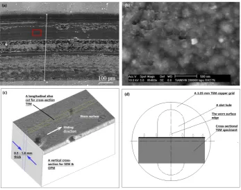
Figure 1. The procedure of sample cutting in preparing a cross-section transmission electron microscope (TEM) foil sample: (a) A typical ball-on-disk wear scar; (reprinted with permission from ref. [23]); (b) A high-magnification scanning electron microscopy (SEM) image taken in the smooth area of the worn surface, seeing the highlighted area in (a); (c) A schematic draw to show the positions of cross-sectional SEM and TEM samples; and, (d) A schematic draw to show a grinding-thinned worn cross-section is glued on a TEM slot grid.
Another special need is to prepare an indicative mark of the outmost worn surface of the prepared sample. In FIB-SEM preparation, a special metal, normally platinum, is deposited on the selected sample area before ion beam cutting. Then, the outmost worn surface can be easily recognised just beneath the platinum layer. For the low-angle ion milling preparation, there is no need to deposit such a metal layer. Instead, a layer of metal deposit is naturally generated accompanying the thinning of the specimen. The mechanism is that, whereas the specimen is polished from its both sides by the ion beam sputtering, the sputtered species both from the bulk specimen and from the copper grid will re-deposit on the outmost surface edge of the cross-section. The thickness of the re-deposited layer increases with the polishing time, which makes it distinctly different from the specimen area in TEM observation. Consequently, the re-deposit can serve as a guide of the outmost worn surface, where various worn surface features are well embedded on the top, including wear induced deformation and delamination, tribofilms, and even loose wear debris. Finally, it is important to make a final cleaning when a thin foil specimen is prepared. The aim of the cleaning is to remove the re-deposited species on the sample area. The cleaning is completed by turning the two ion guns of the PIPS instrument to a higher angle of ±10° and running at low energy of 2–3 keV for up to 1 min. Then, the specimen foil to be observed in TEM will be clean at atomic scale, being free from any contaminant dots.
6. A Few Examples
6.1. FEG-SEM Observation on the Running-In Friction
Previous research has revealed the effect of chemical composition and relative humidity (RH) on the friction and wear properties of transition metal nitride coatings in unlubricated pin-on-disk
Figure 1.The procedure of sample cutting in preparing a cross-section transmission electron microscope
(TEM) foil sample: (a) A typical ball-on-disk wear scar; (reprinted with permission from ref. [23]); (b) A high-magnification scanning electron microscopy (SEM) image taken in the smooth area of the worn surface, seeing the highlighted area in (a); (c) A schematic draw to show the positions of cross-sectional SEM and TEM samples; and, (d) A schematic draw to show a grinding-thinned worn cross-section is glued on a TEM slot grid.
Another special need is to prepare an indicative mark of the outmost worn surface of the prepared sample. In FIB-SEM preparation, a special metal, normally platinum, is deposited on the selected sample area before ion beam cutting. Then, the outmost worn surface can be easily recognised just beneath the platinum layer. For the low-angle ion milling preparation, there is no need to deposit such a metal layer. Instead, a layer of metal deposit is naturally generated accompanying the thinning of the specimen. The mechanism is that, whereas the specimen is polished from its both sides by the ion beam sputtering, the sputtered species both from the bulk specimen and from the copper grid will re-deposit on the outmost surface edge of the cross-section. The thickness of the re-deposited layer increases with the polishing time, which makes it distinctly different from the specimen area in TEM observation. Consequently, the re-deposit can serve as a guide of the outmost worn surface, where various worn surface features are well embedded on the top, including wear induced deformation and delamination, tribofilms, and even loose wear debris. Finally, it is important to make a final cleaning when a thin foil specimen is prepared. The aim of the cleaning is to remove the re-deposited species on the sample area. The cleaning is completed by turning the two ion guns of the PIPS instrument to a higher angle of±10◦and running at low energy of 2–3 keV for up to 1 min. Then, the specimen foil to be observed in TEM will be clean at atomic scale, being free from any contaminant dots.
6. A Few Examples
6.1. FEG-SEM Observation on the Running-In Friction
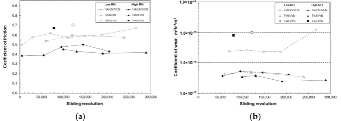
tests [23,28,42]. Figure2shows a collection of some obtained results of average coefficients of friction and wear for a number of coatings. The tests were undertaken at different times and under the same conditions of applied load 5 N, linear sliding speed 0.01 m·s−1, room temperature at two levels of RH (27% and 66% respectively), and against an alumina ball of 6 mm in diameter. The coatings were grown on a pre-polished high speed steel M2 using unbalanced magnetron sputtering. Prior to the sputtering deposition, the samples were ion-etched to enhance the coating-substrate adhesion property using either cathodic arc or high power impulse magnetron [4,28]. In Figure1a, the vanadium-containing coatings TiAlN/VN and TiAlCN/VCN show low coefficients of friction between 0.38 and 0.5 when the tests were undertaken at high RH (66%). Their coefficients of friction became higher and increased to around 0.6, when the RH value was low (27%). The TiAlCrYN coating, however, exhibited high coefficients of friction 0.65–0.7, regardless of the RH values. Correspondingly, the coatings exhibited different coefficients of wear, Figure1b. In general, low friction has been found to contribute to low wear rate.
Lubricants 2018, 6, x FOR PEER REVIEW 8 of 19
wear tests [23,28,42]. Figure 2 shows a collection of some obtained results of average coefficients of friction and wear for a number of coatings. The tests were undertaken at different times and under the same conditions of applied load 5 N, linear sliding speed 0.01 m·s−1, room temperature at two
levels of RH (27% and 66% respectively), and against an alumina ball of 6 mm in diameter. The coatings were grown on a pre-polished high speed steel M2 using unbalanced magnetron sputtering. Prior to the sputtering deposition, the samples were ion-etched to enhance the coating-substrate adhesion property using either cathodic arc or high power impulse magnetron [4,28]. In Figure 1a, the vanadium-containing coatings TiAlN/VN and TiAlCN/VCN show low coefficients of friction between 0.38 and 0.5 when the tests were undertaken at high RH (66%). Their coefficients of friction became higher and increased to around 0.6, when the RH value was low (27%). The TiAlCrYN coating, however, exhibited high coefficients of friction 0.65–0.7, regardless of the RH values. Correspondingly, the coatings exhibited different coefficients of wear, Figure 1b. In general, low friction has been found to contribute to low wear rate.
[image:9.595.124.472.276.400.2](a) (b)
Figure 2. The friction and wear properties of various transition metal nitride coatings in unlubricated pin-on-disk tribotests: (a) average coefficient of friction; and, (b) coefficient of wear.
[image:9.595.198.398.587.721.2]Extensive worn surface analyses revealed the existence of thin tribofilms on the worn surfaces, which strongly adhered to the worn nitride surfaces and replaced the latter in the direct sliding contact. Consequently, the tribofilms eventually determined the coefficient of friction. A series of interrupted sliding wear tests were designed to correlate the variation of friction to the evolution of the sliding contact zone, i.e., the worn surface. Figure 3 shows an example of the running-in friction curves. In the experiments, the tribotests were terminated at total sliding periods of 10, 20, 100, 500, and 1000 cycles to obtain a series of wear tracks for examination. Details of the results have been published elsewhere [25,26], whereas a few typical images are presented in this paper in order to demonstrate the use of high-resolution SEM in the wear mechanism study.
Figure 3. The running-in period of the friction curve of a TiAlN/VN coating measured in an unlubricated pin-on-disk sliding test versus an alumina ball. The ‘X’ marks in the curve denote the terminating points for SEM observation of worn surface, namely, 10, 20, 100, and 500 sliding cycles.
Figure 2.The friction and wear properties of various transition metal nitride coatings in unlubricated
pin-on-disk tribotests: (a) average coefficient of friction; and, (b) coefficient of wear.
Extensive worn surface analyses revealed the existence of thin tribofilms on the worn surfaces, which strongly adhered to the worn nitride surfaces and replaced the latter in the direct sliding contact. Consequently, the tribofilms eventually determined the coefficient of friction. A series of interrupted sliding wear tests were designed to correlate the variation of friction to the evolution of the sliding contact zone, i.e., the worn surface. Figure3shows an example of the running-in friction curves. In the experiments, the tribotests were terminated at total sliding periods of 10, 20, 100, 500, and 1000 cycles to obtain a series of wear tracks for examination. Details of the results have been published elsewhere [25,26], whereas a few typical images are presented in this paper in order to demonstrate the use of high-resolution SEM in the wear mechanism study.
Lubricants 2018, 6, x FOR PEER REVIEW 8 of 19
wear tests [23,28,42]. Figure 2 shows a collection of some obtained results of average coefficients of friction and wear for a number of coatings. The tests were undertaken at different times and under the same conditions of applied load 5 N, linear sliding speed 0.01 m·s−1, room temperature at two
levels of RH (27% and 66% respectively), and against an alumina ball of 6 mm in diameter. The coatings were grown on a pre-polished high speed steel M2 using unbalanced magnetron sputtering. Prior to the sputtering deposition, the samples were ion-etched to enhance the coating-substrate adhesion property using either cathodic arc or high power impulse magnetron [4,28]. In Figure 1a, the vanadium-containing coatings TiAlN/VN and TiAlCN/VCN show low coefficients of friction between 0.38 and 0.5 when the tests were undertaken at high RH (66%). Their coefficients of friction became higher and increased to around 0.6, when the RH value was low (27%). The TiAlCrYN coating, however, exhibited high coefficients of friction 0.65–0.7, regardless of the RH values. Correspondingly, the coatings exhibited different coefficients of wear, Figure 1b. In general, low friction has been found to contribute to low wear rate.
(a) (b)
Figure 2. The friction and wear properties of various transition metal nitride coatings in unlubricated pin-on-disk tribotests: (a) average coefficient of friction; and, (b) coefficient of wear.
Extensive worn surface analyses revealed the existence of thin tribofilms on the worn surfaces, which strongly adhered to the worn nitride surfaces and replaced the latter in the direct sliding contact. Consequently, the tribofilms eventually determined the coefficient of friction. A series of interrupted sliding wear tests were designed to correlate the variation of friction to the evolution of the sliding contact zone, i.e., the worn surface. Figure 3 shows an example of the running-in friction curves. In the experiments, the tribotests were terminated at total sliding periods of 10, 20, 100, 500, and 1000 cycles to obtain a series of wear tracks for examination. Details of the results have been published elsewhere [25,26], whereas a few typical images are presented in this paper in order to demonstrate the use of high-resolution SEM in the wear mechanism study.
Figure 3. The running-in period of the friction curve of a TiAlN/VN coating measured in an unlubricated pin-on-disk sliding test versus an alumina ball. The ‘X’ marks in the curve denote the terminating points for SEM observation of worn surface, namely, 10, 20, 100, and 500 sliding cycles.
Figure 3. The running-in period of the friction curve of a TiAlN/VN coating measured in an
Figures4–6provides the application of SEM SE imaging in the observation of worn surfaces. The imaging mode has very powerful spatial resolution in resolving nano-scale features, owing to the field emission gun and the SE imaging mode.
Lubricants 2018, 6, x FOR PEER REVIEW 9 of 19
[image:10.595.181.412.143.325.2]Figures 4–6 provides the application of SEM SE imaging in the observation of worn surfaces. The imaging mode has very powerful spatial resolution in resolving nano-scale features, owing to the field emission gun and the SE imaging mode.
[image:10.595.92.508.377.719.2]Figure 4. A high magnification field emission gun (FEG)-SEM image taken at the boundary of the 100-sliding-cycle wear track to show the as-deposited coating surface.
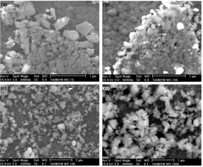
Figure 5. High magnification FEG-SEM secondary electron (SE) images showing the evolution of TiAN/VN wear debris after different sliding cycles against a WC counterpart ball: (a) 10 cycles; (b) 100 cycles; (c) 10,000 cycles; and, (d) 100,000 cycles.
X
Figure 4. A high magnification field emission gun (FEG)-SEM image taken at the boundary of the
100-sliding-cycle wear track to show the as-deposited coating surface.
Lubricants 2018, 6, x FOR PEER REVIEW 9 of 19
Figures 4–6 provides the application of SEM SE imaging in the observation of worn surfaces. The imaging mode has very powerful spatial resolution in resolving nano-scale features, owing to the field emission gun and the SE imaging mode.
Figure 4. A high magnification field emission gun (FEG)-SEM image taken at the boundary of the 100-sliding-cycle wear track to show the as-deposited coating surface.
Figure 5. High magnification FEG-SEM secondary electron (SE) images showing the evolution of TiAN/VN wear debris after different sliding cycles against a WC counterpart ball: (a) 10 cycles; (b) 100 cycles; (c) 10,000 cycles; and, (d) 100,000 cycles.
X
Figure 5. High magnification FEG-SEM secondary electron (SE) images showing the evolution of
Lubricants 2018, 6, x FOR PEER REVIEW 10 of 19
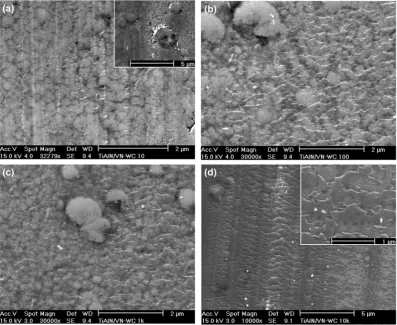
Figure 6. High magnification FEG-SEM SE images showing the evolution of TiALN/VN worn surface after different sliding cycles against a WC counterpart ball: (a) 10 cycles; (b) 100 cycles; (c) 1000 cycles; and, (d) 10,000 cycles. Note the kinetic process of tribofilm formation. The arrows label the sliding direction of the counterpart.
The micrograph in Figure 4 delivers two important features, namely the nano-scale cellular-like growth front of the coating and the preferential wear of a large defect grain. The cellular-like cells refer to columnar grains when the coating was grown under a relatively low substrate bias voltage. Hard coatings with such rough surface refer to dense columns with sub-dense column boundaries, which favours relatively low residual compressive stresses and promise better wear performance when the coating is deposited on a machining tool [22]. With respect to the sliding wear, such nano-scale rough surface facilitate asperity contacting mode in the beginning of the pin-on-disk tribotest. In other words, the applied normal and tangential loads were applied on only a small portion of the nominal contacting area, so that high concentrated loads were applied on a limited number of column grain tops to result in breakage, fracture, and spalling wear of these nitride grains. Secondly, a large growth defect grain in the middle of the imaged area had been flattened by wear, seeing the area labelled with a ‘X’ mark. The small flat worn area is adhered with a transferred layer of the counterpart material, WC cemented carbide. Some agglomerated fine WC particles adjacent to the worn area. The small worn area provided an evidence of the initial wear that is caused by asperity contact between the coating surface and the counterpart ball. Such asperity contacts took place only at a limited number of contacting points, and thereafter, resulted in highly concentrated contact stresses.
The micrographs in Figure 5 were taken on the edges of wear tracks after various selected sliding cycles to demonstrate the evolution of wear debris with increasing sliding cycles. The initial wear particles are in sub-micron scale, which were caused by the breakage of the column tops, as described above. Some of the initial particles were accommodated along the wear track edge, whereas some were entrapped into the sliding contact zone to subject to further breaking and
Figure 6.High magnification FEG-SEM SE images showing the evolution of TiALN/VN worn surface
after different sliding cycles against a WC counterpart ball: (a) 10 cycles; (b) 100 cycles; (c) 1000 cycles; and, (d) 10,000 cycles. Note the kinetic process of tribofilm formation. The arrows label the sliding direction of the counterpart.
The micrograph in Figure4delivers two important features, namely the nano-scale cellular-like growth front of the coating and the preferential wear of a large defect grain. The cellular-like cells refer to columnar grains when the coating was grown under a relatively low substrate bias voltage. Hard coatings with such rough surface refer to dense columns with sub-dense column boundaries, which favours relatively low residual compressive stresses and promise better wear performance when the coating is deposited on a machining tool [22]. With respect to the sliding wear, such nano-scale rough surface facilitate asperity contacting mode in the beginning of the pin-on-disk tribotest. In other words, the applied normal and tangential loads were applied on only a small portion of the nominal contacting area, so that high concentrated loads were applied on a limited number of column grain tops to result in breakage, fracture, and spalling wear of these nitride grains. Secondly, a large growth defect grain in the middle of the imaged area had been flattened by wear, seeing the area labelled with a ‘X’ mark. The small flat worn area is adhered with a transferred layer of the counterpart material, WC cemented carbide. Some agglomerated fine WC particles adjacent to the worn area. The small worn area provided an evidence of the initial wear that is caused by asperity contact between the coating surface and the counterpart ball. Such asperity contacts took place only at a limited number of contacting points, and thereafter, resulted in highly concentrated contact stresses.
entrapped into the sliding contact zone to subject to further breaking and powdering. In Figure5a–d, the wear particles can be seen to be increasingly smaller when the sliding proceeded to more cycles, most of them eventually becoming nano-scale agglomerates.
The micrographs in Figure6demonstrate the generation of tribo-oxide films on the worn surface with increasing sliding cycles. Initially, dispersive nanoscale attachments formed on the worn surface, Figure6a. These extremely fine attachments are nitride debris that strongly adhered to the worn surface because of the strong ionic bonding of the transition metal nitride. The attachments increased in amount and in continuity with the increased sliding cycles, seeing Figure6b,c, and eventually generated a continuous film, seeing Figure6d. The tribofilm exhibit fish-scale morphology. Such morphology suggests adhesive flow of the tribofilm being driven by the tangential load, in which the responsive frictional resistance depends strongly on the shear resistance of the tribofilm. More details about the formation of tribofilms have been published elsewhere [26]. In addition to the adhesive attachments and tribofilm, Figure6also shows some loose debris rods. These rods, along with the edges of the fish-scales, exhibit bright contrast due to the concentrated generation of secondary electrons. Previously, the FIB technique was employed to prepare a cross-sectional TEM foil to characterize the structure and chemistry of such rods. The rods were found to be amorphous multicomponent oxide of the TiAlN/VN nitride [21].
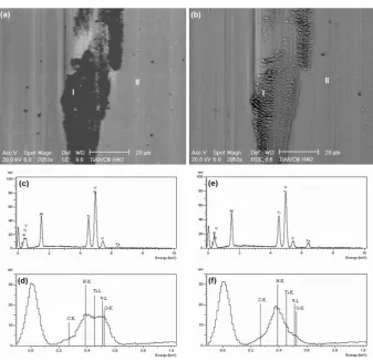
Figure7demonstrates the application of SEM BSE and SE imaging modes and EDX analysis in the characterization of tribo-oxide products. The images were taken on the worn surface of a TiAlCN/VCN coating generated after about 150,000 cycles of unlubricated sliding against an alumina ball. Details of the coating deposition and the tribological properties have been published elsewhere [28].
Lubricants 2018, 6, x FOR PEER REVIEW 11 of 19
powdering. In Figure 5a–d, the wear particles can be seen to be increasingly smaller when the sliding proceeded to more cycles, most of them eventually becoming nano-scale agglomerates.
The micrographs in Figure 6 demonstrate the generation of tribo-oxide films on the worn surface with increasing sliding cycles. Initially, dispersive nanoscale attachments formed on the worn surface, Figure 6a. These extremely fine attachments are nitride debris that strongly adhered to the worn surface because of the strong ionic bonding of the transition metal nitride. The attachments increased in amount and in continuity with the increased sliding cycles, seeing Figure 6b,c, and eventually generated a continuous film, seeing Figure 6d. The tribofilm exhibit fish-scale morphology. Such morphology suggests adhesive flow of the tribofilm being driven by the tangential load, in which the responsive frictional resistance depends strongly on the shear resistance of the tribofilm. More details about the formation of tribofilms have been published elsewhere [26]. In addition to the adhesive attachments and tribofilm, Figure 6 also shows some loose debris rods. These rods, along with the edges of the fish-scales, exhibit bright contrast due to the concentrated generation of secondary electrons. Previously, the FIB technique was employed to prepare a cross-sectional TEM foil to characterize the structure and chemistry of such rods. The rods were found to be amorphous multicomponent oxide of the TiAlN/VN nitride [21].
[image:12.595.129.467.380.706.2]Figure 7 demonstrates the application of SEM BSE and SE imaging modes and EDX analysis in the characterization of tribo-oxide products. The images were taken on the worn surface of a TiAlCN/VCN coating generated after about 150,000 cycles of unlubricated sliding against an alumina ball. Details of the coating deposition and the tribological properties have been published elsewhere [28].
Figure 7. Analysis of worn surface and tribofilm by means of three SEM modes: (a) the SEM SE imaging mode; (b) SEM back-scattered electron (BSE) imaging mode; (c,e) the SEM-energy dispersive X-ray (EDX) spectroscopic analysis of tribofilm; and (d,f) the SEM-EDX spectroscopic analysis of the worn nitride surface.
Figure 7. Analysis of worn surface and tribofilm by means of three SEM modes: (a) the SEM SE
In the SE image, Figure7a, the imaged area shows mainly two levels of contrast. The smooth worn surface of the nitride exhibits grey contract whereas a piece of tribo-oxide film exhibits dark contrast. The different contrast derived from the fact that these two areas emitted different amounts of secondary electrons, i.e., stronger SE signals were generated in the nitride area than in the tribo-oxide area. The significant difference in the SE emission implies different chemical structure of the tribofilm to the nitride.
In the BSE image, Figure7b, the tribofilm exhibits slightly brighter contrast than the nitride worn surface, which reflects the similarity in the mass density between the nitride and the tribo-oxide. Moreover, the tribofilm also shows fine features, which suggests the discontinuity in mass when considering its nature in the dynamic formation by repeated shear deforming and agglomerating. The dark-contrast areas in the tribofilm can be then interpreted as the porous volumes in the tribofilm. Figure7c–f show the comparative SEM-EDX analysis of the two regions. The only difference between the two regions is in the low-energy period of the spectra, i.e., the presence of light elements O and N. So, the profiles of the light element spectra are highlighted to show more details in better energy resolution. In the spectra of the nitride worn surface, Figure6d,f, the spectroscopic peak is dominated by N–K although lower intensity C and O are also within the peak width. The low-energy peak of the tribofilm, Figure7c,e, seems to be overlapped subpeaks of N–K and O–K, which can be interpreted as the occurrence of tribo-oxidation.
In Figure7c–f, the limitation of EDX analysis is obviously in the poor energy resolution. In the acquisition, the whole band of 10 keV is accommodated in about 1000 channels, which derives a resolution of approximately 10 eV per channel. When considering the factor of peak broadening, such poor resolution, is unable to separate the characteristic X-rays of N–K (392 eV), Ti–L (452 eV), V–L (511 eV), and O–K (525 eV). More comprehensive characterization is available in TEM-EELS analysis, to be discussed in later section.
6.2. TEM, EDX, and EELS Analysis of Tribofilms
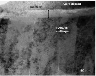
Using TEM to analyse the tribofilm on a worn surface, the first step is to prepare a cross-sectional TEM sample. The sample shown in this case study was a worn surface of a magnetron sputtered TiAlN/VN multilayer coating, which was tested in a ball-on-disc dry sliding wear against an alumina ball [14,22–24] after 200,000 sliding cycles. The cross-sectional TEM foil sample was prepared through a procedure from manual grinding and polishing to ion milling using a PIPS instrument (Model: Gatan 691). A typical cross-sectional TEM bright field image is shown in Figure8. As described before, the top edge of the image is a layer of copper redeposit that is generated by sputtered sample materials (including the slot copper grid, the steel substrate, as well as the nitride coating). Then, beneath the copper redeposit is the whole section of the tribofilm and the top part of the TiAlN/VN coating. Each part has been clearly labelled in Figure8.
Full details of the scientific findings of the research can be found in previous publications [14,22,23]. The focus of this paper is mainly on the interpretation of the acquired EDX and EELS results.
the spectrum of the wear debris to the best energy resolution, Figure9d, where the maximum point of the peak corresponds to the energy level of O–K.
Lubricants 2018, 6, x FOR PEER REVIEW 13 of 19
[image:14.595.136.461.130.387.2]This has been confirmed by resolving the spectrum of the wear debris to the best energy resolution, Figure 9d, where the maximum point of the peak corresponds to the energy level of O–K.
[image:14.595.97.504.446.641.2]Figure 8. A cross-sectional TEM bright field micrograph of the worn TiAlN/VN multilayer coating, showing the whole thickness of a tribofilm attached on the worn TiAlN/VN top.
Figure 9. TEM-EDX spectra acquired in the cross-sectional worn TiAlN/VN samples: (a) in the TiAlN/VN multilayer; (b) in the tribofilm; and (c,d) in the wear debris.
In Figure 10, selected EELS patterns are illustrated in order to interpret the chemical characteristics of the nitrides TiAlN/VN and VN, the tribofilm, and the wear debris. These patterns were acquired in the same samples as those in Figure 8. Several important features should be addressed. Firstly, the EELS exhibit much higher energy resolution than EDX spectroscopy that the energy edges of N–K, Ti–L, V–L, and O–K are well separated to each other. Note that the whole energy width in each pattern is only 250 eV, which is much smaller than the corresponding EDX spectra. Thus, EELS makes it possible to feature the different presence of N, O, given their very close energy bands to the Ti–L and V–L bands. Secondly, EELS exhibits its great sensibility in
Figure 8.A cross-sectional TEM bright field micrograph of the worn TiAlN/VN multilayer coating,
showing the whole thickness of a tribofilm attached on the worn TiAlN/VN top.
Lubricants 2018, 6, x FOR PEER REVIEW 13 of 19
This has been confirmed by resolving the spectrum of the wear debris to the best energy resolution, Figure 9d, where the maximum point of the peak corresponds to the energy level of O–K.
Figure 8. A cross-sectional TEM bright field micrograph of the worn TiAlN/VN multilayer coating, showing the whole thickness of a tribofilm attached on the worn TiAlN/VN top.
Figure 9. TEM-EDX spectra acquired in the cross-sectional worn TiAlN/VN samples: (a) in the TiAlN/VN multilayer; (b) in the tribofilm; and (c,d) in the wear debris.
In Figure 10, selected EELS patterns are illustrated in order to interpret the chemical characteristics of the nitrides TiAlN/VN and VN, the tribofilm, and the wear debris. These patterns were acquired in the same samples as those in Figure 8. Several important features should be addressed. Firstly, the EELS exhibit much higher energy resolution than EDX spectroscopy that the energy edges of N–K, Ti–L, V–L, and O–K are well separated to each other. Note that the whole energy width in each pattern is only 250 eV, which is much smaller than the corresponding EDX spectra. Thus, EELS makes it possible to feature the different presence of N, O, given their very close energy bands to the Ti–L and V–L bands. Secondly, EELS exhibits its great sensibility in
Figure 9. TEM-EDX spectra acquired in the cross-sectional worn TiAlN/VN samples: (a) in the
TiAlN/VN multilayer; (b) in the tribofilm; and (c,d) in the wear debris.
makes it possible to feature the different presence of N, O, given their very close energy bands to the Ti–L and V–L bands. Secondly, EELS exhibits its great sensibility in detecting light elements. In the patterns, both N and O show distinct and strong energy edges with substantial intensities as compared to the edges of metal elements. However, the EELS patterns of TiAlN/VN and VN show N–K edge only, but no O–K edge. On the other hand, the O–K edges in the tribofilm and wear debris are fairly strong, indicating the occurrence of tribo-oxidation. Note that the N–K band in Figure10d is flattened, indicating the complete oxidation of the wear debris. Thirdly, the high energy resolution of EELS facilitate the detailed comparison of an energy edge shape between different chemical compounds, i.e., the energy loss near-edge structure or ELNES. It is worthwhile to compare the N–K edge in the three patterns. The N–K edge of the VN and TiAlN/VN, both being stoichiometric nitrides, shows two sharp peaks at the energies of 400 and 420 eV, respectively, and one broad peak at 430 eV. In the N–K of the tribofilm, only the first peak remains the similar shape whereas the other two peaks became less than half the intensity of the stoichiometric nitrides. According to literature of similar EELS analysis, such modified ELNES suggests the loss of nitrogen in the compound, i.e., the nitride becoming sub-stoichiometric. In other words, the nitrides in the tribofilm were in an intermediate chemical state of the tribo-oxidation.
Lubricants 2018, 6, x FOR PEER REVIEW 14 of 19
[image:15.595.95.503.314.633.2]detecting light elements. In the patterns, both N and O show distinct and strong energy edges with substantial intensities as compared to the edges of metal elements. However, the EELS patterns of TiAlN/VN and VN show N–K edge only, but no O–K edge. On the other hand, the O–K edges in the tribofilm and wear debris are fairly strong, indicating the occurrence of tribo-oxidation. Note that the N–K band in Figure 10d is flattened, indicating the complete oxidation of the wear debris. Thirdly, the high energy resolution of EELS facilitate the detailed comparison of an energy edge shape between different chemical compounds, i.e., the energy loss near-edge structure or ELNES. It is worthwhile to compare the N–K edge in the three patterns. The N–K edge of the VN and TiAlN/VN, both being stoichiometric nitrides, shows two sharp peaks at the energies of 400 and 420 eV, respectively, and one broad peak at 430 eV. In the N–K of the tribofilm, only the first peak remains the similar shape whereas the other two peaks became less than half the intensity of the stoichiometric nitrides. According to literature of similar EELS analysis, such modified ELNES suggests the loss of nitrogen in the compound, i.e., the nitride becoming sub-stoichiometric. In other words, the nitrides in the tribofilm were in an intermediate chemical state of the tribo-oxidation.
Figure 10. TEM-electron energy loss spectroscopy (EELS) acquired in the cross-sectional worn TiAlN/VN samples: (a) in the TiAlN/VN multilayer; (b) in the tribofilm; and, (c,d) in the wear debris. Reprinted with permission from ref. [14].
6.3. XTEM of Wear Induced Subsurface Microstructure Changes
In sliding wear, the applied normal and tangential loads are known to cause plastic deformation of the surfaces in sliding contact, which resulted in hardening due to dislocation interactions and softening due to frictional heating depending on the applied conditions. Delamination wear is often observed to take place in the deformed layer as a result of the deformation induced hardening. The depth of deformation depends strongly on the hardness of the worn surface. As stated before, cross-sectional microscopy provided an effective method to characterize such wear failure by observing the resultant microstructural evolution from the
Figure 10. TEM-electron energy loss spectroscopy (EELS) acquired in the cross-sectional worn
TiAlN/VN samples: (a) in the TiAlN/VN multilayer; (b) in the tribofilm; and, (c,d) in the wear debris. Reprinted with permission from ref. [14].
6.3. XTEM of Wear Induced Subsurface Microstructure Changes
The depth of deformation depends strongly on the hardness of the worn surface. As stated before, cross-sectional microscopy provided an effective method to characterize such wear failure by observing the resultant microstructural evolution from the outmost surface to certain depth. In the case of PVD hard coatings in which the depth of deformation is within sub-micron or nano-scales, cross-sectional TEM has often been applied to study such wear mechanisms. In preparing such cross-sectional TEM foil, it is important to take great care in the manual grinding stage of sample preparation to prevent any artificial damage of the sample, e.g., avoiding cracking and spalling of the original worn surface edge. Also, it should be strictly prohibited to have the ion beam bombard the worn surface in the PIPS ion milling stage. Then, the real worn surface features can be retained for the TEM observation. In addition, the observed foil area should be thin enough to ensure high quality of TEM observation.
Some examples are provided in Figure11. Detailed experimental work has been published elsewhere [17–19,67]. Figure11a–c were taken from the worn surface of a TiAlCrYN coating when the prepared cross-sectional foil sample was observed using a high-voltage JEOL 3010 TEM at 300 KV. The high accelerating voltage facilitated observation of relatively thick sample. The worn surface deformation can be seen to have taken place in a depth of sub-micron scale, seeing the bended columnar grains towards the sliding direction (indicated by an arrow in Figure10a). When comparing to the BF imaging, a better way is the use of dark field imaging to highlight the bending deformation of the columnar grains, e.g., comparing Figure11b,c. The delamination cracks were easy to recognize because of the much higher brightness than the coating matrix caused by direct transmission of electron beam.
Lubricants 2018, 6, x FOR PEER REVIEW 15 of 19
outmost surface to certain depth. In the case of PVD hard coatings in which the depth of deformation is within sub-micron or nano-scales, cross-sectional TEM has often been applied to study such wear mechanisms. In preparing such cross-sectional TEM foil, it is important to take great care in the manual grinding stage of sample preparation to prevent any artificial damage of the sample, e.g., avoiding cracking and spalling of the original worn surface edge. Also, it should be strictly prohibited to have the ion beam bombard the worn surface in the PIPS ion milling stage. Then, the real worn surface features can be retained for the TEM observation. In addition, the observed foil area should be thin enough to ensure high quality of TEM observation.
[image:16.595.93.501.359.610.2]Some examples are provided in Figure 11. Detailed experimental work has been published elsewhere [17–19,67]. Figure 11a–c were taken from the worn surface of a TiAlCrYN coating when the prepared cross-sectional foil sample was observed using a high-voltage JEOL 3010 TEM at 300 KV. The high accelerating voltage facilitated observation of relatively thick sample. The worn surface deformation can be seen to have taken place in a depth of sub-micron scale, seeing the bended columnar grains towards the sliding direction (indicated by an arrow in Figure 10a). When comparing to the BF imaging, a better way is the use of dark field imaging to highlight the bending deformation of the columnar grains, e.g., comparing Figure 11b,c. The delamination cracks were easy to recognize because of the much higher brightness than the coating matrix caused by direct transmission of electron beam.
Figure 11. Cross-sectional TEM images showing deformation and delamination wear of nitride coatings: (a) A BF image of TiAlCrYN coating; (b,c) bright field (BF) and dark field (DF) images of TiAlCrYN coating; (d,e) BF images of TiAlN/CrN coating. Reprinted with permission from refs. [17,18].
Figure 11d,e are cross-sectional TEM images of a multilayer coating TiAlN/CrN. The TiAlN/CrN coated block sample was tested in a block-on-ring dry sliding manner against a cylindrical surface of hardened steel. The images were taken using a Philips CM20 TEM working at 200 KV. The BF images show wear induced bending deformation, cracks, and a nanoscale delamination sheet. In Figure 11d, a Fe–O based tribofilm can be seen on the top worn surface. Its nanocrystalline nature was revealed in the BF imaging, whereas selected area diffraction analysis confirmed the predominant presence of Fe3O4 oxide (Figure 4 in Ref. [18]). In another place of the same worn surface, the TiAlN/CrN coating showed delamination wear. A typical delamination
Figure 11.Cross-sectional TEM images showing deformation and delamination wear of nitride coatings:
(a) A BF image of TiAlCrYN coating; (b,c) bright field (BF) and dark field (DF) images of TiAlCrYN coating; (d,e) BF images of TiAlN/CrN coating. Reprinted with permission from refs. [17,18].
showed delamination wear. A typical delamination sheet is shown in Figure11e, which is only about 10 nm thick, forming a big contrast to the severe delamination of TiAlCrYN coating (Figure11a–c).
7. Summary
Friction and wear are known to generate wear debris and tribofilms along with other phenomena on the worn surfaces. A comprehensive understanding of the mechanisms of wear and friction can be achieved by careful analyses of these wear products. Electron microscopy and associated spectroscopic analyses provide a powerful tool in the comprehensive characterization of these wear products.
Of these, SEM based imaging and spectroscopic analyses are straight forward in assessing worn surfaces and wear debris, where FEG-SEM is capable of observing wear induced features in up to nano-scale, and the BSE imaging and EDX spectroscopy are applied to deal with tribo-chemical wear.
TEM based wear mechanism study has been attributed to the successful preparation of cross-sectional worn surface samples using the ion beam milling techniques. On the prepared cross-sectional samples, TEM provides sufficiently high spatial resolution in observing wear induced microstructure changes in certain depths of the worn surface layer, including tribofilms and other types of worn surface attachments. More importantly, TEM has been a very useful platform to combine BF and DF imaging, SAD, EDX, EELS, and ELNES in the multiple analyses of wear mechanisms.
Funding:This research received no external funding.
Acknowledgments: Zhaoxia Zhou, University of Sheffield, is acknowledged for providing the instrument
operation in the TEM-EELS analysis.
Conflicts of Interest:The authors declare no conflict of interest.
References
1. Münz, W.D. Titanium aluminium nitride films—A new alternative to TiN coatings.J. Vac. Sci. Technol.1986, 4, 2717–2725. [CrossRef]
2. Paldeys, S.; Deevi, S.C. Single layer and multilayer wear resistant coatings of (Ti,Al)N: A review. Mater. Sci. Eng.2003,A342, 58–79. [CrossRef]
3. Helmersson, U.; Todorova, S.; Barnett, S.A.; Sandgren, J.E.; Markert, J.C.; Greene, J.E. Growth of single-crystal TiN/VN strained-layer superlattices with extremely high mechanical hardness. J. Appl. Phys. 1987, 62, 481–484. [CrossRef]
4. Münz, W.D.; Donohue, L.A.; Hovsepian, P.E. Properties of various large-scale fabricated TiAlN- and CrN-based superlattice coatings grown by combined cathodic arc-unbalanced magnetron sputter deposition. Surf. Coat. Technol.2000,125, 269–277. [CrossRef]
5. Veprek, S.; Reiprich, S.; Li, S. Superhard nanocrystalline composite materials: The TiN/Si3N4 system. Appl. Phys. Lett.1995,66, 2640–2642. [CrossRef]
6. Lu, C.; Mai, Y.M.; Shen, Y.G. Recent advances on understanding the origin of superhardness in nanocomposite coatings: A critical review.J. Mater. Sci.2006,41, 937–950. [CrossRef]
7. Musil, J. Physical and mechanical properties of hard nanocomposite films prepared by reactive magnetron sputtering. In Nanostructured Hard Coatings; De Hosson, J.T.M., Cavaleiro, A., Eds.; Springer Science: Berlin, Germany, 2006; pp. 407–463.
8. Martınez-Martınez, D.; Lopez-Cartes, C.; Justo, A.; Fernandez, A.; Sanchez-Lopez, J.C. Self-lubricating Ti–C–N nanocomposite coatings prepared by double magnetron sputtering.Solid State Sci.2009,11, 660–670. [CrossRef]
9. Lu, Y.H.; Shen, Y.G. Nanostructure transition: From solid solution Ti(N,C) to nanocomposite nc-Ti(N,C)/ a-(C,CNx).Appl. Phys. Lett.2007,90, 221913. [CrossRef]
10. Erdemir, A.; Donnet, C. Tribology of diamond-like carbon films: Recent progress and future prospects. J. Phys. D Appl. Phys.2006,39, R311–R327. [CrossRef]
12. Merkle, A.P.; Erdemir, A.; Eryilmaz, O.L.; Johnson, J.A.; Marks, L.D. In situ TEM studies of tribo-induced bonding modifications in near-frictionless carbon films.Carbon2010,48, 587–591. [CrossRef]
13. Lindquist, M.; Wilhelmsson, O.; Jansson, U.; Wiklund, U. Tribofilm formation and tribological properties of TiC and nanocomposite TiAlC coatings.Wear2009,266, 379–387. [CrossRef]
14. Luo, Q.; Zhou, Z.; Rainforth, W.M.; Hovsepian, P.E. TEM-EELS study of low-friction superlattice TiAlN/VN coating: The wear mechaisms.Tribol. Lett.2006,24, 171–178. [CrossRef]
15. Luo, Q.; Xie, J.P.; Song, Y.P. Effects of microstructure on the abrasive wear behaviour of spheroidal cast iron. Wear1995,184, 1–10. [CrossRef]
16. Luo, Q.; Xie, J.P.; Lu, W. Investigation of the wear failure mechanism of a flour milling roller.Wear1993, 161, 11–16. [CrossRef]
17. Luo, Q.; Rainforth, W.M.; Münz, W.D. TEM observation of wear mechanisms of TiAlCrN and TiAlN/CrN coatings grown by combined steered-arc/unbalanced magnetron deposition. Wear1999,225–229, 74–82. [CrossRef]
18. Luo, Q.; Rainforth, W.M.; Münz, W.D. TEM study of the wear of TiAlN/CrN superlattice coatings. Scrip. Mater.2001,45, 399–404. [CrossRef]
19. Luo, Q.; Rainforth, W.M.; Münz, W.D. Wear mechanisms of monolithic and multicomponent nitride coatings grown by combined arc etching and unbalanced magnetron sputtering.Surf. Coat. Technol.2001,146–147, 430–435. [CrossRef]
20. Inman, I.A.; Datta, S.; Du, H.L.; Burnell-Gray, J.S.; Luo, Q. Microscopy of glazed layers formed during high temperature sliding wear.Wear2003,254, 461–467. [CrossRef]
21. Zhou, Z.; Mckay, S.; Luo, Q.; Rainforth, M.; Chen, L.; Hovsepian, P. Investigating Worn Surface of NanoscaleTiAlN/VN Coating Using FIB and TEM.EMAG-Nano Imaging Anal. Fabr. Nanoscale J. Phys. Ser. 2006,26, 95–98.
22. Luo, Q.; Hovsepian, P.E. Transmission electron microscopy and energy dispersive X-ray spectroscopy on the worn surface of nano-structured TiAlN/VN multilayer coating. Thin Solid Films2006,497, 203–209. [CrossRef]
23. Luo, Q.; Zhou, Z.; Rainforth, W.M.; Bolton, M. Effect of tribofilm formation on the dry sliding friction and wear properties of magnetron sputtered TiAlCrYN coatings.Tribol. Lett.2009,34, 113–124. [CrossRef] 24. Luo, Q.; Schimpf, C.; Ehiasarian, A.P.; Chen, L.; Hovsepian, P.E. Structure and wear mechanisms of
nano-structured TiAlCN/VCN multilayer coatings.Plasma Processes Polym.2007,4, S916–S920. [CrossRef] 25. Luo, Q. Tribofilms in solid lubricants. In Encyclopedia of Tribology; Wang, Q.J., Chung, Y.-W., Eds.;
Springer Science: New York, NY, USA, 2013; pp. 3760–3767.
26. Luo, Q. Origin of friction in running-in sliding wear of nitride coatings. Tribol. Lett. 2010,37, 529–539. [CrossRef]
27. Zhou, Z.; Rainforth, W.M.; Luo, Q.; Hovsepian, P.E.; Ojeda, J.J.; Romero-Gonzalez, M.E. Wear and friction of TiAlN/VN coatings against Al2O3in air at room and elevated temperatures.Acta Mater.2010,58, 2912–2925. [CrossRef]
28. Luo, Q.; Wang, S.C.; Zhou, Z.; Chen, L. Structure characterization and tribological study of magnetron sputtered nanocompositenc-TiAlV(N,C)/a-C coatings.J. Mater. Chem.2011,21, 9746–9756. [CrossRef] 29. Luo, Q. Temperature dependent friction and wear of magnetron sputtered coating TiAlN/VN.Wear2011,
271, 2058–2066. [CrossRef]
30. Abbasi, E.; Luo, Q.; Owens, D. Cast study: Wear mechanisms of NiCrVMo-steel and CrB-steel scrap shear blades.Wear2018,398–399, 29–40. [CrossRef]
31. Ibrahim, M.Z.; Sarhan, A.A.D.; Yusuf, F.; Hamdi, M. Biomedical materials and techniques to improve the tribological, mechanical and biomedical properties of orthopaedic implants—A review article. J. Alloy. Compd.2017,714, 636–667. [CrossRef]
32. Van Hove, R.P.; Sierevelt, I.N.; van Royen, B.J.; Nolte, P.A. Titanium nitride coating of orthopaedic implants: A review of the literature.BioMed. Res. Int.2015,2015, 1–9. [CrossRef] [PubMed]
34. Affatato, S.; Roggiero, A.; De Mattia, J.S.; Taddei, P. Does metal transfer affect the tribological behaviour of demoral heads? Roughness and phase transformation analyses on retrieved zirconia and Biolox Delta composites.Compos. Part B2016,92, 290–298. [CrossRef]
35. Namus, R.; Zheng, P.; Rainforth, W.M. Correlation of the wear transition in CoCrMo alloys with the formation of a nanocrystalline surface layer and a proteinaceous surface film.Wear2017,376–377, 223–231. [CrossRef] 36. Zeng, P.; Rana, A.; Thompson, R.; Rainforth, W.M. Subsurface characterisation of wear on mechanically
polished and electro-polished bilmedical grade CoCrMo.Wear2015,332–333, 650–661. [CrossRef]
37. Yan, Y.; Wang, L.; Neville, A.; Qiao, L. (iv) Tribofilm on hip implants. Orthop. Trauma2013,27, 93–100. [CrossRef]
38. Slonaker, M.; Goswami, T. Review of wear mechnaisms in hip implants: Paper II—Ceramics IG004712. Mater. Des.2004,25, 395–405. [CrossRef]
39. Zeng, P.; Rainforth, W.M.; Inkson, B.J.; Stewart, T.D. Transmission electron microscopy analysis of worn alumina hip replacement prostheses.Acta Mater.2012,60, 2061–2072. [CrossRef]
40. Zeng, P.; Rainforth, W.M.; Stewart, T.D. Characterisation of the wear mechanisms in retrieved aluminium-on-alumina total hip replacements.Wear2017,376–377, 212–222. [CrossRef]
41. Luo, Q.; Lewis, D.B.; Hovsepian, P.E.; Münz, W.D. Transmission electron microscopy and X-ray diffrac-tion investigation of the microstructure of nano-scale multilayers TiAlN/VN grown by unbalanced magne-tron deposition.J. Mater. Res.2004,19, 1093–1104. [CrossRef]
42. Lewis, D.B.; Creasey, S.; Zhou, Z.; Forsyth, J.J.; Ehiasarian, A.P.; Hovsepian, P.E.; Luo, Q.; Rainforth, W.M.; Münz, W.M. The effect of (Ti + Al): V ratio on the structure and oxidation behavior of TiAlN/VN nano-scale multilayer coatings.Surf. Coat. Technol.2004,177–178, 252–259. [CrossRef]
43. Hovsepian, P.E.; Lewis, D.B.; Luo, Q.; Münz, W.D.; Mayrhofer, P.H.; Mitterer, C.; Zhou, Z.; Rainforth, W.M. TiAlN based nanoscale multilayer PVD coatings designed to adapt their tribological properties at elevated temperatures.Thin Solid Films2005,485, 160–168. [CrossRef]
44. Luo, Q.; Robinson, G.; Pittman, M.; Howarth, M.; Sim, W.M.; Stalley, M.R.; Leitner, H.; Ebner, R.; Caliskanoglu, D.; Hovsepian, P.E. Performance of nano-structured multilayer PVD coating TiAlN/VN in dry high speed milling of aerospace aluminium 7010-T7651. Surf. Coat. Technol. 2005,200, 123–127. [CrossRef]
45. Luo, Q.; Hovsepian, P.E.; Lewis, D.B.; Münz, W.D.; Kok, Y.N.; Cockrem, J.; Bolton, M.; Farinotti, A. Tribological perperties of unbalanced magnetron sputtered nanoscale multilayer coatings TiAlN/VN and TiAlCrYN deposited on plasma nitrided steels.Surf. Coat. Technol.2005,193, 39–45. [CrossRef]
46. Dave, D.; Krug, T.; Tietema, R.; Sim, W.; Luo, Q.; Hovsepian, P.E. New Tool Coatings for Light Metal Cutting. Trans. Mater. Heat Treat.2004,25, 832–836.
47. Lewis, D.B.; Luo, Q.; Zhou, Z.; Hovsepian, P.E.; Münz, W.D. Interrelationship between atomic species, bias voltage, texture and microstructure of nano-scale multilayers.Surf. Coat. Technol.2004,184, 225–232. [CrossRef]
48. Leyens, C.; Peters, M.; Hovsepian, P.E.; Lewis, D.B.; Luo, Q.; Münz, W.D. Novel Coating Systems Produced by the Combined Cathodic Arc/Unbalanced Magnetron Sputtering for Environmental Protection of Titanium Alloys and Titanium Aluminides.Surf. Coat. Technol.2002,155, 103–111. [CrossRef]
49. Luo, Q.; Oluwafemi, O.; Kitchen, M.; Yang, S. Tribological properties and wear mechanisms of DC pulse plasma nitrided austenitic stainless steel in dry reciprocating sliding tests.Wear2017,376–377, 1640–1651. [CrossRef]
50. Sigle, W. Analytical transmission electron microscopy.Ann. Rev. Mater. Res.2005,35, 239–314. [CrossRef] 51. Ponsonnet, L.; Donnet, C.; Varlot, K.; Martin, J.M.; Grill, A.; Tatel, V. EELS analysis of hydrogenated
diamond-like carbon films.Thins Solid Films1998,319, 97–100. [CrossRef]
52. Mitternauer, C.; Hebert, C.; Kothleitner, G.; Hofer, F.; Schattschnerder, P.; Zandbergen, H.W. Electron energy loss near edge structure as a fingerprint for identifying chromium nitrides. Solid State Commun. 2004, 130, 209–213. [CrossRef]
53. Kothleitner, G.; Rogers, M.; Berendes, A.; Bock, W.; Kolbesen, B.O. A combined SNMS and EFTEM/EELS study on focused ion beam prepared vanadium nitride thin films.Appl. Surf. Sci.2005,252, 66–76. [CrossRef] 54. Van Benthem, K.; Kohl, H. Methods for ELNES-quantification: Characterization of the degree of inversion of

![Figure 11.[17,18]. ) A BF image of TiAlCrYN coating; (d) BF images of TiAlN/CrN coating](https://thumb-us.123doks.com/thumbv2/123dok_us/686999.571690/16.595.93.501.359.610/figure-image-tialcryn-coating-images-tialn-crn-coating.webp)
