© MOTOROLA 2004
This document contains information on a new product. Specifications and information herein are subject to change without notice.
Product Proposal
16-Bit Microcontroller
Based on Motorola’s market-leading flash technology, members of the MC9S12C-Family deliver the power and flexibility of our 16 Bit core (CPU12) family to a whole new range of cost and space sensitive, general purpose Industrial and Automotive network applications. MC9S12C-Family members are com-prised of standard on-chip peripherals including a 16-bit central processing unit (CPU12), up to 128K bytes of Flash EEPROM or ROM, up to 4K bytes of RAM, an asynchronous serial communications in-terface (SCI), a serial peripheral inin-terface (SPI), an 8-channel 16-bit timer module (TIM), a 6-channel 8-bit Pulse Width Modulator (PWM), an 8-channel, 10-bit analog-to-digital converter (ADC) and up to one CAN 2.0 A, B software compatible module (MSCAN12). The MC9S12C-Family has full 16-bit data paths throughout. The inclusion of a PLL circuit allows power consumption and performance to be ad-justed to suit operational requirements. In addition to the I/O ports available in each module, up to 10 dedicated I/O port bits are available with Wake-Up capability from STOP or WAIT mode. The MC9S12C-Family is available in 48, 52 and 80 pin QFP packages, with the 80 Pin version pin compat-ible to the HCS12 B and D- Family derivatives.
The C-Family includes ROM versions MC3S12C128/96/64/32/16 of all devices which provide a further cost reduction path for applications with high volume and stable code.
Features
• 16-bit HCS12 CORE — HCS12 CPU
— MMC (memory map and interface) — INT (interrupt control)
— BDM (background debug mode)
— DBG12 (enhanced debug12 module including breakpoints and change-of-flow trace buffer) — Multiplexed Expansion Bus (available only in 80 pin package version)
• 16-bit HCS12 CPU
— Upward compatible with M68HC11 instruction set
— Interrupt stacking and programmer’s model identical to M68HC11 — Instruction queue
— Enhanced indexed addressing • Wake-up interrupt inputs
— Up to 10-port bits available for wake up interrupt function • Memory options
— 16K, 32K, 64K, 96K and 128K Byte Flash EEPROM (erasable in 512-byte sectors) or — 16K, 32K, 64K, 96K and 128K Byte ROM
— 2K and 4K Byte RAM • Analog-to-Digital Converters
— One 8-channel module with 10-bit resolution. — External conversion trigger capability
• Up to one 1M bit per second, CAN 2.0 A, B software compatible modules — Five receive and three transmit buffers
F
re
e
sc
a
le
S
e
m
ic
o
n
d
u
c
to
r,
I
For More Information On This Product, Go to: www.freescale.com
n
c
.
— Flexible identifier filter programmable as 2 x 32 bit, 4 x 16 bit or 8 x 8 bit — Four separate interrupt channels for receive, transmit, error and wake-up — Low-pass filter wake-up function
— Loop-back for self test operation • Timer Module (TIM)
— 16-bit Counter with 7-bit Prescaler
— 8 programmable input capture or output compare channels — Simple PWM Mode
— Modulo Reset of Timer Counter — 16-Bit Pulse Accumulator — External Event Counting — Gated Time Accumulation • 6 PWM channels
— Programmable period and duty cycle — 8-bit 6-channel or 16-bit 3-channel
— Separate control for each pulse width and duty cycle — Center-aligned or left-aligned outputs
— Programmable clock select logic with a wide range of frequencies — Fast emergency shutdown input
• Serial interfaces
— One asynchronous serial communications interface (SCI) — One synchronous serial peripheral interface (SPI)
• CRG (Clock Reset Generator Module) — Windowed COP watchdog,
— Real time interrupt, — Clock monitor, — Clock generation — Reset Generation
— Phase-locked loop clock frequency multiplier — Limp home mode in absence of external clock
— Low power 0.5 to 16 MHz crystal oscillator reference clock • Operation frequency
— 32MHz equivalent to 16MHz Bus Speed for single chip
— 32MHz equivalent to 16MHz Bus Speed in expanded bus modes — Option: 50MHz equivalent to 25MHz Bus Speed
• Internal 2.5V Regulator
— Supports an input voltage range from 3.3V-10% to 5.5V — Low power mode capability
— Includes low voltage reset (LVR) circuitry — Includes low voltage interrupt (LVI) circuitry • 48-Pin LQFP, 52-Pin LQFP or 80-Pin QFP package
— Up to 58 I/O lines with 5V input and drive capability — Up to 2 dedicated 5V input only lines (IRQ, XIRQ) — 5V A/D converter inputs and 5V I/O
• Development support
— Single-wire background debug™ mode (BDM) — On-chip hardware breakpoints
— Enhanced DBG12 debug features
F
re
e
sc
a
le
S
e
m
ic
o
n
d
u
c
to
r,
I
n
c
.
MC9S12C-Family MOTOROLA
PRODUCT PROPOSAL, Rev. 3, 12-May-04 3
• Pin out explanations:
— I/O is the sum of ports capable to act as digital input or output.
For 80 Pin Versions:
Port A = 8, B = 8, E = 6 + 2 input only, J = 2, M = 6, P = 8, S = 4, T = 8, PAD = 8. 12 inputs provide Interrupt capability (P= 8, J = 2, IRQ, XIRQ)
For 52 Pin Versions:
Port A = 3, B = 1, E = 2 + 2 input only, M = 6, P = 3, S = 2, T = 8, PAD = 8. 5 inputs provide Interrupt capability (P= 3, IRQ, XIRQ)
For 48 Pin Versions:
Port A = 1, B = 1, E = 2 + 2 input only, M = 6, P = 1, S = 2, T = 8, PAD = 8. 3 inputs provide Interrupt capability (P= 1, IRQ, XIRQ)
128K 0 4K
48LQFP MC9S12C128 1 1 1 8ch 6ch 8ch 31
52LQFP MC9S12C128 1 1 1 8ch 6ch 8ch 35
80QFP MC9S12C128 1 1 1 8ch 6ch 8ch 60
96K 0 4K
48LQFP MC9S12C96 1 1 1 8ch 6ch 8ch 31
52LQFP MC9S12C96 1 1 1 8ch 6ch 8ch 35
80QFP MC9S12C96 1 1 1 8ch 6ch 8ch 60
64K 0 4K
48LQFP MC9S12C64 1 1 1 8ch 6ch 8ch 31
52LQFP MC9S12C64 1 1 1 8ch 6ch 8ch 35
80QFP MC9S12C64 1 1 1 8ch 6ch 8ch 60
32K 0 2K
48LQFP MC9S12C32 1 1 1 8ch 6ch 8ch 31
52LQFP MC9S12C32 1 1 1 8ch 6ch 8ch 35
80QFP MC9S12C32 1 1 1 8ch 6ch 8ch 60
32K 0 2K 48LQFP MC9S12GC32 0 1 1 8ch 6ch 8ch 31
52LQFP MC9S12GC32 0 1 1 8ch 6ch 8ch 35
16K 0 2K 48LQFP MC9S12GC16 0 1 1 8ch 6ch 8ch 31
52LQFP MC9S12GC16 0 1 1 8ch 6ch 8ch 35
0 128K 4K
48LQFP MC3S12C128 1 1 1 8ch 6ch 8ch 31
52LQFP MC3S12C128 1 1 1 8ch 6ch 8ch 35
80QFP MC3S12C128 1 1 1 8ch 6ch 8ch 60
0 96K 4K
48LQFP MC3S12C96 1 1 1 8ch 6ch 8ch 31
52LQFP MC3S12C96 1 1 1 8ch 6ch 8ch 35
80QFP MC3S12C96 1 1 1 8ch 6ch 8ch 60
0 64K 4K
48LQFP MC3S12C64 1 1 1 8ch 6ch 8ch 31
52LQFP MC3S12C64 1 1 1 8ch 6ch 8ch 35
80QFP MC3S12C64 1 1 1 8ch 6ch 8ch 60
0 32K 2K
48LQFP MC3S12C32 1 1 1 8ch 6ch 8ch 31
52LQFP MC3S12C32 1 1 1 8ch 6ch 8ch 35
80QFP MC3S12C32 1 1 1 8ch 6ch 8ch 60
0 32K 2K 48LQFP MC3S12GC32 0 1 1 8ch 6ch 8ch 31
52LQFP MC3S12GC32 0 1 1 8ch 6ch 8ch 35
0 16K 2K 48LQFP MC9S12GC16 0 1 1 8ch 6ch 8ch 31
52LQFP MC9S12GC16 0 1 1 8ch 6ch 8ch 35
F
re
e
sc
a
le
S
e
m
ic
o
n
d
u
c
to
r,
I
For More Information On This Product, Go to: www.freescale.com
n
c
.
[image:3.612.74.541.89.560.2]Figure 1 Block Diagram
32K, 64K, 96K, 128K Byte Flash/ROM
2K, 4K Byte RAM
MSCAN VDDR VDDA VSSA VRH VRL ATD AN2 AN6 AN0 AN7 AN1 AN3 AN4 AN5 PAD3 PAD4 PAD5 PAD6 PAD7 PAD0 PAD1 PAD2 IOC2 IOC6 IOC0 IOC7 IOC1 IOC3 IOC4 IOC5 PT3 PT4 PT5 PT6 PT7 PT0 PT1 PT2 RXCAN TXCAN SCK MISO PS3 PS0 PS1 PS2 SS SPI PTAD PTT DDR T PTS DDRS Voltage Regulator VDD1 VSS1 PWM
Signals shown in Bold are not available on the 52 or 48 Pin Package
D DRAD VDDA VSSA Timer Module VDDX VSSX VRH VRL VSSR RESET EXTAL XTAL BKGD R/W MODB/IPIPE1 XIRQ NOACC/XCLKS System Integration Module (SIM) HCS12 Periodic Interrupt COP Watchdog Clock Monitor Single-wire Background PLL VSSPLL XFC VDDPLL
Multiplexed Address/Data Bus
Multiplexed Wide Bus IRQ LSTRB/TAGLO ECLK MODA/IPIPE0 PA 4 PA 3 PA 2 PA 1 PA 0 PA 7 PA 6 PA 5 TEST/VPP ADD R1 2 ADD R1 1 ADD R1 0 ADD R9 ADDR8 ADD R1 5 ADD R1 4 ADD R1 3 DA T A 1 2 DA T A 1 1 DA T A 1 0 DA T A 9 DA T A 8 DA T A 1 5 DA T A 1 4 DA T A 1 3
PB4 PB3 PB2 PB1 PB0
PB7 PB6 PB5
ADDR4 ADD R3 ADD R2 ADD R1 ADD R0 ADD R7 ADD R6 ADD R5 DA T A 4 DA T A 3 DA T A 2 DA T A 1 DA T A 0 DA T A 7 DA T A 6 DA T A 5 PE3 PE4 PE5 PE6 PE7 PE0 PE1 PE2 DDRA DDRB PTA PTB DDRE PTE Clock and Reset Generation Module Debug12 Module VDD2 VSS2
Signals shown in Bold Italic are available in the 52, but not the 48 Pin Package
CPU PM3 PM4 PM5 PM0 PM1 PM2 PTM DDR M PW2 PW0 PW1 PW3 PW4 PW5 PP3 PP4 PP5 PP6 PP7 PP0 PP1 PP2 PTP DDRP PJ6 PJ7 PTJ DD RJ VDD1,2 VSS1,2 VDDX VSSX Internal Logic 2.5V
VDDPLL VSSPLL PLL 2.5V
I/O Driver 5V
VDDA VSSA A/D Converter 5V
VDDR VSSR
Voltage Regulator 5V & I/O
VRL is bonded internally to VSSA for 52 and 48 Pin packages
MOSI Module Keypa d Interr upt Key Int
SCI RXD
MC9S12C-Family MOTOROLA
[image:5.612.93.502.86.415.2]PRODUCT PROPOSAL, Rev. 3, 12-May-04 5
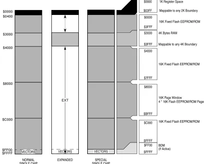
Figure 2 MCxS12C128 User Configurable Memory Map
$FFFF $C000 $8000 $4000 $0400
$FF00
EXT
NORMAL SINGLE CHIP
EXPANDED SPECIAL
SINGLE CHIP VECTORS
VECTORS
$FF00 $FFFF
BDM (If Active) $C000
$FFFF
16K Fixed Flash EEPROM/ROM $8000
$BFFF
16K Page Window
8 * 16K Flash EEPROM/ROM Pages $4000
$7FFF
16K Fixed Flash EEPROM/ROM $3000
$3FFF Mappable to any 4K Boundary 4K Bytes RAM
$3000
The figure shows a useful map, which is not the map out of reset. After reset the map is: $0000 - $03FF: Register Space
$0000 - $0FFF: 4K RAM (only 3K visible $0400 - $0FFF)
$0000
$3FFF
16K Fixed Flash EEPROM/ROM
VECTORS
Flash Erase Sector Size is 1024 Bytes
F
re
e
sc
a
le
S
e
m
ic
o
n
d
u
c
to
r,
I
For More Information On This Product, Go to: www.freescale.com
n
c
.
Figure 3 MCxS12C96 User Configurable Memory Map
$0000
$FFFF $C000 $8000 $4000 $0400
$FF00
EXT
NORMAL SINGLE CHIP
EXPANDED SPECIAL
SINGLE CHIP VECTORS
VECTORS
$FF00 $FFFF
BDM (If Active) $C000
$FFFF
16K Fixed Flash EEPROM/ROM $8000
$BFFF
16K Page Window
6 * 16K Flash EEPROM/ROM Pages $4000
$7FFF
16K Fixed Flash EEPROM/ROM $3000
$3FFF $0000
$03FF
1K Register Space
Mappable to any 2K Boundary
Mappable to any 4K Boundary 4K Bytes RAM
$3000
The figure shows a useful map, which is not the map out of reset. After reset the map is: $0000 - $03FF: Register Space
$0000 - $0FFF: 4K RAM (only 3K visible $0400 - $0FFF)
$0000
$3FFF
16K Fixed Flash EEPROM/ROM
VECTORS
Flash Erase Sector Size is 1024 Bytes
F
re
e
sc
a
le
S
e
m
ic
o
n
d
u
c
to
r,
I
n
c
.
MC9S12C-Family MOTOROLA
[image:7.612.93.502.86.415.2]PRODUCT PROPOSAL, Rev. 3, 12-May-04 7
Figure 4 MCxS12C64 User Configurable Memory Map
$FFFF $C000 $8000 $4000 $0400
$FF00
EXT
NORMAL SINGLE CHIP
EXPANDED SPECIAL
SINGLE CHIP VECTORS
VECTORS
$FF00 $FFFF
BDM (If Active) $C000
$FFFF
16K Fixed Flash EEPROM/ROM $8000
$BFFF
16K Page Window
4 * 16K Flash EEPROM/ROM Pages $4000
$7FFF
16K Fixed Flash EEPROM/ROM $3000
$3FFF Mappable to any 4K Boundary 4K Bytes RAM
$3000
The figure shows a useful map, which is not the map out of reset. After reset the map is: $0000 - $03FF: Register Space
$0000 - $0FFF: 4K RAM (only 3K visible $0400 - $0FFF)
$0000
$3FFF
16K Fixed Flash EEPROM/ROM
VECTORS
Flash Erase Sector Size is 512 Bytes
F
re
e
sc
a
le
S
e
m
ic
o
n
d
u
c
to
r,
I
For More Information On This Product, Go to: www.freescale.com
n
c
.
Figure 5 MCxS12C32 User Configurable Memory Map
$0000
$FFFF $C000 $8000 $4000 $0400
$FF00
EXT
NORMAL SINGLE CHIP
EXPANDED SPECIAL
SINGLE CHIP VECTORS
VECTORS
$FF00 $FFFF
BDM (If Active) $C000
$FFFF
16K Fixed Flash EEPROM/ROM $8000
$BFFF
16K Page Window
2 * 16K Flash EEPROM/ROM Pages $3800
$3FFF $0000
$03FF
1K Register Space
Mappable to any 2K Boundary
Mappable to any 2K Boundary 2K Bytes RAM
$3800
The figure shows a useful map, which is not the map out of reset. After reset the map is: $0000 - $03FF: Register Space
$0800 - $0FFF: 2K RAM
VECTORS
Flash Erase Sector Size is 512 Bytes
F
re
e
sc
a
le
S
e
m
ic
o
n
d
u
c
to
r,
I
n
c
.
MC9S12C-Family MOTOROLA
[image:9.612.100.501.82.418.2]PRODUCT PROPOSAL, Rev. 3, 12-May-04 9
Figure 6 MCxS12C16 User Configurable Memory Map
$FFFF $C000 $8000 $4000 $0400
$FF00
EXT
NORMAL SINGLE CHIP
EXPANDED SPECIAL
SINGLE CHIP VECTORS
VECTORS
$FF00 $FFFF
BDM (If Active) $C000
$FFFF
16K Fixed Flash EEPROM/ROM $8000
$BFFF
16K Page Window
1 * 16K Flash EEPROM/ROM Page $3800
$3FFF Mappable to any 2K Boundary 2K Bytes RAM
$3800
The figure shows a useful map, which is not the map out of reset. After reset the map is: $0000 - $03FF: Register Space
$0800 - $0FFF: 2K RAM
VECTORS
Flash Erase Sector Size is 512 Bytes
F
re
e
sc
a
le
S
e
m
ic
o
n
d
u
c
to
r,
I
For More Information On This Product, Go to: www.freescale.com
n
c
.
Figure 7 Pin Assignments in 80 QFP for MC9S12C-Family
!!! Pin-out is Subject to Change!!! 1
2 3 4 5 6 7 8 9 10 11 12 13 14 15 16 17 18 19 20
80 79 78 77 76 75 74 73 72 71 70 69 68 67 66 65 64 63 62 61
21 22 23 24 25 26 27 28 29 30 31 32 33 34 35 36 37 38 39 40 MC9S12C-Family
80 QFP
VRH VDDA PAD07/AN07 PAD06/AN06 PAD05/AN05 PAD04/AN04 PAD03/AN03 PAD02/AN02 PAD01/AN01 PAD00/AN00 VSS2 VDD2
PA7/ADDR15/DATA15 PA6/ADDR14/DATA14 PA5/ADDR13/DATA13 PA4/ADDR12/DATA12 PA3/ADDR11/DATA11 PA2/ADDR10/DATA10 PA1/ADDR9/DATA9 PA0/ADDR8/DATA8
PP4/KWP4/PW4 PP5/KWP5/PW5 PP7/KWP7 VDDX VSSX PM0/RXCAN PM1/TXCAN PM2/MISO PM3/SS PM4/MOSI PM5/SCK PJ6/
KWJ6
PJ7/
KWJ7
PP6/KWP6/R
OMONE
PS3 PS2 PS1/TXD PS0/RXD VSSA VRL
PW3/KWP3/PP3 PW2/KWP2/PP2 PW1/KWP1/PP1 PW0/KWP0/PP0 PW0/IOC0/PT0 PW1/IOC1/PT1 PW2/IOC2/PT2 PW3/IOC3/PT3 VDD1 VSS1 PW4/IOC4/PT4 IOC5/PT5 IOC6/PT6 IOC7/PT7 MODC/TAGHI/BKGD ADDR0/DATA0/PB0 ADDR1/DATA1/PB1 ADDR2/DATA2/PB2 ADDR3/DATA3/PB3 ADDR4/DATA4/PB4
ADDR5/D
A
TA5
/PB5
ADDR6/D
A
TA6
/PB6
ADDR7/D
A
TA7
/PB7
XCLKS
/NO
A
CC
/PE7
MODB/IPIPE1
/PE6
MOD
A
/IPIPE0
/PE5
ECLK
/PE4 VSSR VDDR RESET
VDDPLL
XFC
VSSPLL EXT
AL
XT
AL
TEST
/VPP
LSTRB
/T
A
G
LO
/PE3
R/W
/PE2
IR
Q
/PE1
XIR
Q
/PE0
60 59 58 57 56 55 54 53 52 51 50 49 48 47 46 45 44 43 42 41
Signals shown in Bold are not available on the 52 or 48 Pin Package Signals shown in Bold Italic are available in the 52, but not the 48 Pin Package
F
re
e
sc
a
le
S
e
m
ic
o
n
d
u
c
to
r,
I
n
c
.
MC9S12C-Family MOTOROLA
[image:11.612.104.475.102.467.2]PRODUCT PROPOSAL, Rev. 3, 12-May-04 11
Figure 8 Pin assignments 52 QFP for MC9S12C-Family
MC9S12C-Family 52 QFP 1
2
3
4
5
6
7
8
9
10
11
12
13
39
38
37
36
35
34
33
32
31
30
29
28
27
14 15 16 17 18 19 20 21 22 23 24 25 26 52 51 50 49 48 47 46 45 44 43 42 41 40
* Signals shown in Bold are not available on the 48 Pin Package PP4/KWP4/PW4 PP5/KWP5/PW5 VDDX VSSX PM
0/RX
CAN
PM1/TXCAN PM2/MISO PM3/SS PM4/MOSI PM5/SCK PS1/TXD PS0/RXD VSSA
VRH
VDDA
PAD07/AN07 PAD06/AN06 PAD05/AN05
PAD04/AN04
PAD03/AN03
PAD02/AN02
PAD01/AN01
PAD00/AN00
PA2
PA1
PA0
XCLKS
/PE7
ECLK
/PE4 VSSR
VDDR RESET
VDDPLL
XFC
VS
SPLL EXT
AL
XT
AL
TEST/V
PP
IRQ
/PE1
XIRQ
/PE0
PW3/KWP3/PP3
PW0/IOC0/PT0
PW1/IOC1/PT1
PW2/IOC2/PT2
PW3/IOC3/PT3
VDD1
VSS1
PW4/IOC4/PT4
IOC5/PT5
IOC6/PT6
IOC7/PT7
MODC/BKGD
PB4
F
re
e
sc
a
le
S
e
m
ic
o
n
d
u
c
to
r,
I
For More Information On This Product, Go to: www.freescale.com
n
c
.
Figure 9 Pin Assignments in 48 LQFP for MC9S12C-Family
MC9S12C-Family 48 LQFP 1
2
3
4
5
6
7
8
9
10
11
12
36
35
34
33
32
31
30
29
28
27
26
25
13 14 15 16 17 18 19 20 21 22 23 24 48 47 46 45 44 43 42 41 40 39 38 37 PP5/KWP5 VDDX VSSX PM
0/RX
CAN
PM1/TXCAN PM2/MISO PM3/SS PM4/MOSI PM5/SCK PS1/TXD PS0/RXD VSSA
PW0/IOC0/PT0
PW1/IOC1/PT1
PW2/IOC2/PT2
PW3/IOC3/PT3
VDD1
VSS1
PW4/IOC4/PT4
IOC5/PT5
IOC6/PT6
IOC7/PT7
MODC/BKGD
PB4
XCLKS
/PE7
ECLK/PE4
VSSR VDDR RESE
T
VDDPLL
XFC
VSSPLL EX
TA
L
XT
AL
TEST/VPP IRQ
/PE1
VRH
VDDA
PAD07/AN07 PAD06/AN06 PAD05/AN05
PAD04/AN04
PAD03/AN03
PAD02/AN02
PAD01/AN01
PAD00/AN00
PA0
XIRQ/PE0
F
re
e
sc
a
le
S
e
m
ic
o
n
d
u
c
to
r,
I
n
c
.
MC9S12C-Family MOTOROLA
[image:13.612.89.558.82.613.2]PRODUCT PROPOSAL, Rev. 3, 12-May-04 13
Figure 10 48-pin LQFP Mechanical Dimensions (case no.932-03 ISSUE F)
A A1
Z 0.200 AC T-U 4X
B B1
1
12
13 24
25 36 37 48
S1 S
V
V1
P
AE AE
T, U, Z DETAIL Y
DETAIL Y
BASE METAL
N J
F D
T-U
M
0.080 AC Z
SECTION AE-AE
AD
G 0.080 AC
M°
TOP & BOTTOM
L°
W
K AA E
C
H
0.
25
0
R 9
DETAIL AD
1. CONTROLLING DIMENSION: MILLIMETER. 2. DATUM PLANE AB IS LOCATED AT BOTTOM
OF LEAD AND IS COINCIDENT WITH THE LEAD WHERE THE LEAD EXITS THE PLASTIC BODY AT THE BOTTOM OF THE PARTING LINE.
3. DATUMS T, U, AND Z TO BE DETERMINED AT DATUM PLANE AB.
4. DIMENSIONS S AND V TO BE DETERMINED AT SEATING PLANE AC.
5. DIMENSIONS A AND B DO NOT INCLUDE MOLD PROTRUSION. ALLOWABLE PROTRUSION IS 0.250 PER SIDE. DIMENSIONS A AND B DO INCLUDE MOLD MISMATCH AND ARE DETERMINED AT DATUM PLANE AB. 6. DIMENSION D DOES NOT INCLUDE DAMBAR
PROTRUSION. DAMBAR PROTRUSION SHALL NOT CAUSE THE D DIMENSION TO EXCEED
T U
Z
AB
AC
GA
UGE PL
A
N
E
DIM A
MIN MAX
7.000 BSC
MILLIMETERS
A1 3.500 BSC
B 7.000 BSC
B1 3.500 BSC
C 1.400 1.600
D 0.170 0.270
E 1.350 1.450
F 0.170 0.230
G 0.500 BSC
H 0.050 0.150
J 0.090 0.200
K 0.500 0.700
M 12 REF
N 0.090 0.160
P 0.250 BSC
L 0 7
R 0.150 0.250
S 9.000 BSC
S1 4.500 BSC
V 9.000 BSC
V1 4.500 BSC
W 0.200 REF
AA 1.000 REF
° ° °
F
re
e
sc
a
le
S
e
m
ic
o
n
d
u
c
to
r,
I
For More Information On This Product, Go to: www.freescale.com
n
c
.
Figure 11 52-pin LQFP Mechanical Dimensions (case no. 848D-03)
F
NOTES:
2. DIMENSIONING AND TOLERANCING PER ANSI
Y14.5M, 1982.
3. CONTROLLING DIMENSION: MILLIMETER
4. DATUM PLANE -H- IS LOCATED AT BOTTOM OF
LEAD AND IS COINCIDENT WITH THE LEAD WHERE THE LEAD EXITS THE PLASTIC BODY AT THE BOTTOM OF THE PARTING LINE.
5. DATUMS -L-, -M- AND -N- TO BE DETERMINED AT
DATUM PLANE -H-.
6. DIMENSIONS S AND V TO BE DETERMINED AT
SEATING PLANE -T-.
7. DIMENSIONS A AND B DO NOT INCLUDE MOLD
PROTRUSION. ALLOWABLE PROTRUSION IS 0.25 (0.010) PER SIDE. DIMENSIONS A AND B DO INCLUDE MOLD MISMATCH AND ARE DETERMINED AT DATUM PLANE
-H-8. DIMENSION D DOES NOT INCLUDE DAMBAR
PROTRUSION. DAMBAR PROTRUSION SHALL NOT CAUSE THE LEAD WIDTH TO EXCEED 0.46 (0.018). MINIMUM SPACE BETWEEN PROTRUSION AND
VIEW AA
AB AB
VIEW Y
SECTION AB-AB
ROTATED 90° CLOCKWISE
DIM A
MIN MAX MIN MAX
INCHES
10.00 BSC 0.394 BSC MILLIMETERS
A1 5.00 BSC 0.197 BSC B 10.00 BSC 0.394 BSC B1 5.00 BSC 0.197 BSC C --- 1.70 --- 0.067 C1 0.05 0.20 0.002 0.008 C2 1.30 1.50 0.051 0.059 D 0.20 0.40 0.008 0.016
E 0.45 0.030
F 0.22 0.35 0.009 0.014 G 0.65 BSC
0.75 0.018
0.026 BSC J 0.07 0.20 0.003 0.008 K 0.50 REF 0.020 REF R1 0.08 0.20 0.003 0.008
S 12.00 BSC 0.472 BSC S1 6.00 BSC 0.236 BSC U 0.09 0.16 0.004 0.006 V 12.00 BSC 0.472 BSC V1 6.00 BSC 0.236 BSC W 0.20 REF 0.008 REF Z 1.00 REF 0.039 REF CL
-X-X=L, M, N
1
13
14 26
27 39 40 52
4X 13 TIPS 4X
N
0.20 (0.008) H L-M 0.20 (0.008) T L-M N
SEATING PLANE
C
0.10 (0.004) T
4Xθ3
4X θ2
S 0.05 (0.002)
0.25 (0.010)
GAGE PLANE
C2
C1
W
K E Z
S L-M M
0.13 (0.005) T N S PLATING
BASE METAL
D
J U
B V
B1
A S
V1
A1 S1
-L-
-N-
-M- -H-
-T-θ1
θ
G
θ1 θ
θ3 θ2
0° 7° 12°
0° 7° 0° --- 0° ---REF 12°REF
3XVIEW Y
VIEW AA
2X R R1
12°REF 12°REF
F
re
e
sc
a
le
S
e
m
ic
o
n
d
u
c
to
r,
I
n
c
.
MC9S12C-Family MOTOROLA
[image:15.612.89.544.65.644.2]PRODUCT PROPOSAL, Rev. 3, 12-May-04 15
Figure 12 80-pin QFP Mechanical Dimensions (case no. 841B) NOTES:
1. DIMENSIONING AND TOLERANCING PER ANSI Y14.5M, 1982.
2. CONTROLLING DIMENSION: MILLIMETER. 3. DATUM PLANE -H- IS LOCATED AT BOTTOM OF
LEAD AND IS COINCIDENT WITH THE LEAD WHERE THE LEAD EXITS THE PLASTIC BODY AT THE BOTTOM OF THE PARTING LINE. 4. DATUMS -A-, -B- AND -D- TO BE
DETERMINED AT DATUM PLANE -H-. 5. DIMENSIONS S AND V TO BE DETERMINED
AT SEATING PLANE -C-.
6. DIMENSIONS A AND B DO NOT INCLUDE MOLD PROTRUSION. ALLOWABLE PROTRUSION IS 0.25 PER SIDE. DIMENSIONS A AND B DO INCLUDE MOLD MISMATCH AND ARE DETERMINED AT DATUM PLANE -H-. 7. DIMENSION D DOES NOT INCLUDE DAMBAR
PROTRUSION. ALLOWABLE DAMBAR PROTRUSION SHALL BE 0.08 TOTAL IN EXCESS OF THE D DIMENSION AT MAXIMUM MATERIAL CONDITION. DAMBAR CANNOT BE LOCATED ON THE LOWER RADIUS OR THE FOOT.
SECTION B-B DETAIL A
80
-A-L
-D-A
S
A-B
M
0.20 H D S
0.05 A-B
S
1 20
21
-B-B V
J
F
N
D
VIEW ROTATED 90°
DETAIL A B
B P
-A-,-B-,-D-E
H
G
M M
DETAIL C
SEATING PLANE
-C-C DATUM
PLANE
0.10
-H-DATUM PLANE
-H-U T
R
Q K
W X DETAIL C
DIM MIN MAX MILLIMETERS
A 13.90 14.10
B 13.90 14.10
C 2.15 2.45
D 0.22 0.38
E 2.00 2.40
F 0.22 0.33
G 0.65 BSC
H --- 0.25
J 0.13 0.23
K 0.65 0.95
L 12.35 REF
M 5 10
N 0.13 0.17
P 0.325 BSC
Q 0 7
R 0.13 0.30
S 16.95 17.45
T 0.13
---U 0
---V 16.95 17.45
W 0.35 0.45
X 1.6 REF
° ° ° °
° S
A-B
M
0.20 C D S
S
A-B
M
0.
20
D
S
H
0.
05
D
S
A-B
M
0.
20
D
S
C
S
A-B
M
0.20 C D S
F
re
e
sc
a
le
S
e
m
ic
o
n
d
u
c
to
r,
I
For More Information On This Product, Go to: www.freescale.com
n
c
.
Motorola reserves the right to make changes without further notice to any products herein. Motorola makes no warranty, representation or guarantee regarding the suitability of its products for any particular purpose, nor does Motorola assume any liability arising out of the application or use of any product or circuit, and specifically disclaims any and all liability, including without limitation consequential or incidental damages. “Typical” parameters can and do vary in different applications. All operating parameters, including “Typicals” must be validated for each customer application by customer’s technical experts. Motorola does not convey any license under its patent rights nor the rights of others. Motorola products are not designed, intended, or authorized for use as components in systems intended for surgical implant into the body, or other applications intended to support or sustain life, or for any other application in which the failure of the Motorola product could create a situation where personal injury or death may occur. Should Buyer purchase or use Motorola products for any such unintended or unauthorized application, Buyer shall indemnify and hold Motorola and its officers, employees, subsidiaries, affiliates, and distributors harmless against all claims, costs, damages, and expenses, and reasonable attorney fees arising out of, directly or indirectly, any claim of personal injury or death associated with such unintended or unauthorized use, even if such claim alleges that Motorola was negligent regarding the design or manufacture of the part. Motorola and are registered trademarks of Motorola, Inc. Motorola, Inc. is an Equal Opportunity/Affirmative Action Employer.
How to reach us:
USA/EUROPE: Motorola Literature Distribution; P.O. Box 5405, Denver, Colorado 80217. 1-303-675-2140
HOME PAGE: http://mcu.motsps.com/
JAPAN: Motorola Japan Ltd.; SPS, Technial Information Center, 3-20-1, Minami-Azabu, Minato-ku, Tokyo 106-8573 Japan.
81-3-3440-3569
ASIA/PACIFIC: Motorola Semiconductors H.K. Ltd.; Silicon Harbour Centre, 2 Dai King Street, Tai Po Industrial Estate,
F
re
e
sc
a
le
S
e
m
ic
o
n
d
u
c
to
r,
I
n
c
.