ISSN (e): 2250-3021, ISSN (p): 2278-8719
Vol. 08, Issue 11 (November. 2018), ||V (III) || PP 49-53
Effect of High-k Gate on the functioning of MOSFET at nano
meter sizes
Dr. S.P. Venu Madhava Rao
Professor, MVSR Engineering College, Corresponding authors: Dr. S.P. Venu Madhava Rao
Abstract: The scaling of MOSFET has undergone very rapidly and the size of the device has become so small that it required changes in the design, material used for the fabrication of the MOSFET etc. As the size of the device has become very small the thickness of the Silicon Dioxide used for Gate has also become very thin. This results in a significant increase in leakage currents of the Gate and reducing the performance of the MOSFET. In this paper several methods have been proposed to optimize the MOSFET design for better performance.
Keywords:
MOSFET, High-k Dielectric, Doping, Gaussian Doping Density, Uniform Doping Density. --- --- Date of Submission: 18-11-2018 Date of acceptance: 04-12-2018 --- ---I.
INTRODUCTION
The dimensional and electrostatic limitations in the MOS deign mandate scaling of the device to meet the predictions as per ITRS (International Technology Road Map for Semiconductors) [1]. Moore’s law predicted an exponential growth in the number of transistors in an Integrated circuit, to meet this requirement the size of the device has to be brought down to increase density, speed and improvement in power because of the increase in the number of transistors being used in a circuit[2]. The performance of the MOS deteriorates as the geometrics of the device are reduced particularly the channel length, in other words the long channel MOS performs better than the short channel MOS. One of the main effects of the reduction in channel size are called short channel effects like – Drain Induced Barrier Lowering, Punch through, Velocity Saturation, Impact Ionization, Surface Scattering and Hot Electron effects. [3-6]. Researchers have come up with several new structures like SOI MOS, but it suffers from threshold voltage degradation with decrease in channel length [7]. At the nano meter sizes the SiO2 (Silicon Di Oxide) used as Gate dielectric has become very thin resulting in Gate leakage current [8]. This current is due to the tunneling of electrons through the SiO2 which is high. This has few side effects – increase in static power consumption and further reduction in the thickness of the SiO2 layer which is not practicable.
The Gate Oxide Capacitance (C) in MOS can be modeled approximately as parallel plate Capacitor and is given by:
𝐶 =𝑘𝜀𝑜𝐴
𝑡 … … … . . (1) Where:
A = Capacitor Area
k = Relative Dielectric Constant of the material εo = permittivity of free space
t = thickness of the capacitor oxide insulator
As seen from the equation (1) the value of t cannot be further reduced to increase the Gate capacitance. The only other alternative is to have a material which has higher value of k replacing the presently used material Silicon Di Oxide. Now the thickness of the Gate Oxide layer can be increased to reduce the Gate leakage currents. For an increased Drain current, the channel length has to be reduced or the Gate Dielectric Capacitance has to be increased or both.
Silicon has a good advantage in that it has a high electrical quality of Si: SiO2 interface [9]. The interface is atomically abrupt where the Silicon atoms are either present in Si or SiO2 [10]. As such any high K material that replaces Silicon must have the same highest electrical quality in terms of roughness and absence of defects in order to avoid scattering carriers. The defects cause the following changes:
1) Charges trapped in the defects shift the Gate threshold voltage of the transistor.
2) The trapped charges change with time, leading to instability of operating characteristics.
3) The trapped charge carriers scatter in the channel and lower the carrier mobility.
International organization of Scientific Research
50 | Page
The dielectric constants have been calculated in the LDA for the various phases of HfO2 and ZrO2. This can be used to understand the differences and the anisotropies. Rignanese [11] found that the tetragonal phase has the largest and most anisotropic K, but not by as much as found by Zhao and Vanderbilt [12]. These calculations were extended to Lanthanides such as Lu2O3 [13].Today’s VLSI industry uses several doping profiles for different applications, chemical compositions and physical characteristics. As the size of the transistors are reducing at a fast pace, the performance of the transistor in terms of its efficiency is reducing equally fast. To improve the performance the transistor has to be remodeled which in general is a costly affair and thus has to be avoided. Some of the modifications can be doping profile, doping technique, Gate modification, Drain to Source channeling effects etc. The doping profile modifications are more effective as they do not change the MOS basic functionality. An ideal doping profile was described by V. A. K. Temple [14] which yields optimum resistance and breakdown voltage. In [15] for the first time substrate calculations and threshold voltage were used to determine the doping profile. In 2011 Wolpert, David and Paul A have shown the effects of temperature on the functioning of MOS devices. An analytical model of a double Gate MOSFET has been designed using S/D lateral Gaussian Doping Profile [16]. Similarly a FinFET with vertical Gaussian Doping Profile has been designed in [17] and Uniform Doping Profile was used in [18]. These papers suggest that the Gaussian Doping Profile has been found more effective than the Uniform Doping Profile.
II.
DESIGN APPROACH
In this paper design of a MOSFET has been presented that is optimized for different high-k Gate materials and different Doping profiles. This paper presents few design suggestions that make the MOSFET work even at nano meter scaling.
The Gate material used in this paper is n+ Poly Silicon and Aluminum. The different doping profiles used are Uniform Doping Density, Gaussian Source / Drain Doping Density and Gaussian S/D & Halo Doping Density.
III.
HIGH PERMITTIVITY GATE DIELECTRICS
The replacement of the SiO2 by high-k dielectric materials is to satisfy material constraints and process integration conditions as the device is scaled down. There are various conditions that are considered while making the choice of a high-k material as the Gate in a MOSFET. There are 2 primary requirements in choosing the Gate material that can replace SiO2:
a) Suitable conduction band offset – needed to provide sufficient barrier
b) Thermal stability
Tantalum Oxide has high permittivity, but the conduction band barrier (0.36 eV) is not sufficient to provide any real advantage over SiO2. A suitable trade-off between the dielectric constant and the conduction band offset is needed for that material to be chosen to replace the SiO2 [19] [20].
Thermal stability is also a very critical property of high-k dielectrics to CMOS technology. The front end
process involves high temperature thermal annealing where the temperature reaches more than 10000C needed
for dopant activation. Most of the high-k materials undergo crystallization at these temperatures. Generally amorphous high-k materials are preferred, Si can be incorporated into the high-k material and addition of Nitrogen can improve thermal stability and prevents dopant penetration. The Table 1 shows some essential parameters for high-k materials and SiO2.
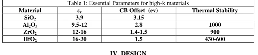
Table 1: Essential Parameters for high-k materials
Material εr CB Offset (ev) Thermal Stability
SiO2 3.9 3.15
Al2O3 9.5-12 2.8 1000
ZrO2 12-16 1.4-1.5 900
HfO2 16-30 1.5 430-600
IV.
DESIGN
In this paper a robust design of the MOSFET has been made and its functionality has been tested for 2 different materials – n+ poly and Aluminum for Uniform Doping Density Profile.
The details are:
Device used : nMOSFET
Doping Profile : Uniform Doping Density Temperature : Ambient (3000K)
Tool used : TCAD Lab from nanohub
The Figure 1 shows the structure of the MOSFET used.
Figure 1: MOSFET Model
The following characteristics are plotted for the MOSFET designed using n+ poly and Aluminium as Gate material:
a) ID-Vg characteristics
b) Surface Charge – Vg characteristics
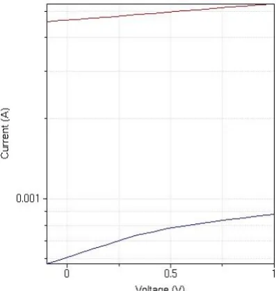
ID-Vg characteristics: These are shown in the Figure 2.
Figure 2(a): ID-Vg characteristics for Gate material of n+ poly silicon
International organization of Scientific Research
52 | Page
Surface Charge – Vg Characteristics: These are shown in Figure 3.Figure 3(a): Surface Charge – Vg characteristics for Gate material of n+ poly Silicon
Figure 3(b): Surface Charge – Vg characteristics for Gate material of Aluminium
REFERENCES
[1]. The International Technology Roadmap for Semiconductor, 2011, Emerging Research Devices.
[2]. S.M. Sze, Physics of Semiconductor Devices, 2nd Edition, 1981, p. 868
[3]. Colinge J P. Silicon on insulator technology: materials to VLSI. 2nd ed. Norwell, MA: Kluwer: Kluwer
Academic Publishers; 1997.
[4]. Mitiko Miura-Mattausch, Hans Jürgen Mattausch,Tatsuya Ezaki, ―The Physics and Modeling of
MOSFET‖, World Scientific Publishing Co. Pte. Ltd., Singapore, 2008.
[5]. G. Venkateshwar Reddy and M. Jagadesh Kumar, ―A New Dual-Material Double-Gate (DMDG)
Nanoscale SOI MOSFET—Two-Dimensional Analytical Modeling and Simulation, IEEE Transactions on Electron Devices, vol..4, no.2, pp.260-268, 2005
[6]. TiyaDeyMalakar, Partha Bhattacharyya, Subir Kumar Sarkar“Analytical Surface Potential Modeling
Based Small Signal Analysis and RF Performance Characterization of DMG SOI MOSFET for Better RFIC Application IETE Technical Review.
[7]. N.H.E. Weste, K. Eshraghian, Principles of CMOS VLSI Design, A System Perspective, Pearson
Education, 2003.
International organization of Scientific Research
53 | Page
[9]. F.J. Himpsel, F.R. McFeely, et. al, Microscopic structure of the SiO2 / Si interface, 1988[10]. J, W, Keister, Band offsets for ultrathin SiO2 and Si3N4 films on Si (111) and Si (100) from photoemission spectroscopy
[11]. Rignanese, G M Gionze, et. al, First- Principles investigation of high-k dielectrics: comparison between the silicates and oxides of Hafnium and Zirconium, Phys. Rev B, 69, 184301
[12]. Zhao, X. and Vanderbilt D, First Principles study of structural, vibrational and lattice dielectric properties of Hafnium Oxide, Phys Rev. B..65, 233106
[13]. Audrius Alkauskas, Peter Broqvist, Fabien Devynck and Alfredo Pasquarello, Band Offsets at
Semiconductor Oxide interfaces from Hybrid Density Functional calculations, Physics Rev. letter, 2008 [14]. V. A. K. Temple, "Ideal FET doping profile," in IEEE Transactions on Electron Devices, vol. 30, no. 6,
pp. 619-626, June 1983.
[15]. D. W. Feldbaumer and D. K. Schroder, "MOSFET doping profiling," in IEEE Transactions on Electron Devices, vol. 38, no. 1, pp. 135-140, Jan 1991.
[16]. A. Nandi, A. K. Saxena and S. Dasgupta, "Analytical Modeling of a Double Gate MOSFET Considering
Source/Drain Lateral Gaussian Doping Profile," in IEEE Transactions on Electron Devices, vol. 60, no. 11, pp. 3705-3709, Nov. 2013.
[17]. Ramesh, R., et al. ―Optical Effects on the Characteristics of GaAs Nanoscale FinFET with Vertical Gaussian Doping Profile.‖ Optik - International Journal for Light and Electron Optics, vol. 124, no. 19, 2013, pp. 4019–4025
[18]. Gowri, K., and V. Rajamani. ―Optical Effects on the Characteristics of a Nanoscale SOI MOSFET with
Uniform Doping Profile.‖ Optik - International Journal for Light and Electron Optics, vol. 125, no. 13, 2014, pp. 3195–3200.
[19]. C.M. Osburn, I. Kim et.al, Vertically scaled MOSFET gate stacks and junctions: how far are we likely to
go?, IBM J. Res & Dev., Vol. 46, No. 2/3, 2002
[20]. E.P. Gusev, E. Cartier, et.al, Ultra thin high-k metal oxides on Silicon: Processing characterization and integration issues, Microelectronic engineering, 59, 2001.