ISSN (Online): 2320-9364, ISSN (Print): 2320-9356
www.ijres.org Volume 4 Issue 10 ǁ October. 2016 ǁ PP.60-66
Design of 600-800 MHz Programmable Phase Locked Loop
Thatipelli shiva, Rita Mahajan,
PEC University Of Technology, Chandigarh, India.PEC University Of Technology, Chandigarh. India
Abstract:
In this paper – emphasis is made on the design and architecture of the Programmable PLL. The frequency range of working of the Programmable PLL is 600-8000MHz with settling times 9, 10, 13 and 20 uSec for the frequencies 600,700,750 and 800 MHz respectively. The programmable PLL is obtained by designing a Programmable frequency divider which has four scale down factors to obtain the desired frequency. The Proposed circuit is designed in 180nm, 3.3 V CMOS technology and simulated using Cadence Virtuoso simulator. There are mainly five parts in the Programmable PLL. They are Phase Detector (PD), Charge Pump (CP), Loop Filter (LP) Voltage control oscillator (VCO) and Programmable frequency divider.Keywords
: programmable PLL, phase detector, voltage control oscillator, charge pump, frequency divider.I.
INTRODUCTION
As the communication technology progresses, the requirement of higher speed lock-up time, smaller size and, low power consumption PLL synthesizers have become crucial in the field of PLL Design. Various procedures and methods have been proposed to attain a high speedlock-up time in a PLL frequency synthesizer 1-4.Loop gain of the PLL has become an important and crucial parameter in PLL design. Many architectures have
been proposed in order to increase the loop gain and to achieve a high speed lock-up time of PLL frequency synthesizers5-6. For example, the fractional division method has been implemented to increase the loop gain7,8. However, in proposed method the usage of two different division ratios alternately have been implemented, the phase noise caused the more spurious noise around the reference frequency even though the loop is in steady state condition. In a conventional PLL, once theprogrammable divider or phase detector is chosen as an element of the PLL9, the loop gain of PLL becomes fixed. In this paper, we propose a new PLL frequency synthesizer with multi-programmable divider which can attain a higher speed lock-up time.
Phase locked loop is a circuit which synchronizes the output frequency with the input reference frequency signal. Programmable PLL consists of mainly five parts. They are Phase Detector (PD), Charge Pump (CP), Loop Filter (LP), Voltage Control Oscillator (VCO) and Programmable Frequency Divider.
2. Dynamics of Charge Pump PLL
In order to enumerate the behavior of charge-Pump PLL a linear model has to be implemented for the combination of the PFD, charge pump and the low-pass filter so as to obtain the transfer function of the combination8. From the observations of the output of the loop filter we can express as
𝑉𝑜𝑢𝑡 𝑡 = 𝐼𝑃
2𝜋𝐶𝑃 𝑡. ∅0𝑢 𝑡 (1.0)
The impulse response of the system is given by eq.1.1 ℎ 𝑡 = 𝐼𝑃
2𝜋𝐶𝑃𝑢 𝑡 (1.1)
The transfer function is given by the following expression 𝑉𝑜𝑢𝑡
∆∅ 𝑠 = 𝐼𝑃 2𝜋𝐶𝑃 .
1
𝑆 (1.2)
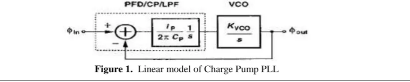
From the above transfer function we can observe that the combination of the PFD/CP/LPF contains a pole at the origin. In analogy, 𝐼𝑃/2𝜋𝐶𝑃 is expressed as the gain of the PFD and denoted as 𝐾𝑃𝐹𝐷. The linear model of the charge-pump PLL can be constructed as shown in Figure1.and the model gives an open-loop transfer function is given by eq.1.3
∅𝑜𝑢𝑡
∅𝑖𝑛 𝑠 |𝑜𝑝𝑒𝑛 = 𝐼𝑃
2𝜋𝐶𝑃
𝐾𝑉𝐶𝑂
𝑆2 (1.3)
Since from the above transfer function it is observed that there are two poles at the origin, Thistype of topology is called a “type II” PLL. The closed loop transfer function is denoted by H(s) for the sake of brevity, is thus equal to
𝐻 𝑠 =
𝐼𝑃 𝐾𝑉𝐶𝑂 2𝜋 𝐶𝑃
𝑆2+𝐼𝑃 𝐾𝑉𝐶𝑂
2𝜋 𝐶𝑃
(1.4)
The result of the transfer is alarming due to the presence of the imaginary poles at 𝑆1,2= ±𝑗 𝐼𝑃 𝐾𝑉𝐶𝑂/2𝜋𝐶𝑃 which makes the loop unstable. The instability of the loop is due to the presence of the poles at the origin which are seen from the open loop of the transfer function of the linear-model. The presence of each pole adds an additional phase of 900, allowing tooscillate at the gain crossover frequency. In order to stabilize the loop we need to modify the phase of the system which can reduce the 1800 phase shift at the gain cross over frequency which is possible by introduction of the zero in the loop gain. This is done by introduction of the resistor in series with the loop filter capacitor which then modifies the PFD/CP/LP transfer function to expression 1.5
𝑉𝑜𝑢𝑡
∆∅ (𝑠) = 𝐼𝑃
2𝜋 𝑅𝑝+ 1
𝐶𝑝𝑠 (1.5)
The open-loop transfer function of the Charge pump PLL is given by eqn.1.6 ∅out
∅𝑖𝑛(s)|open = 𝐼𝑃
2𝜋 𝑅𝑝+ 1 𝐶𝑝𝑠
𝐾𝑉𝐶𝑂
𝑆 (1.6) And hence
𝐻 𝑆 =
𝐼𝑃 𝐾𝑉𝐶𝑂
2𝜋 𝐶𝑃 (𝑅𝑝𝐶𝑝𝑠+1)
𝑆2+𝐼𝑃
2𝜋𝐾𝑉𝐶𝑂𝑅𝑝𝑆+2𝜋 𝐶𝑃𝐼𝑃 𝐾𝑉𝐶𝑂
(1.7)
The closed loop system contains a zero at Sz= -1/ (𝑅𝑝𝐶𝑝). Using the same notation as that for the type I PLL, we have
𝜔𝑛 = 𝐼𝑃 𝐾𝑉𝐶𝑂
2𝜋𝐶𝑃 (1.8)
𝜁 = 𝑅𝑝
2
𝐼𝑃 𝐶𝑝𝐾𝑉𝐶𝑂
2𝜋 (1.9)
3. Components of PLL
The various components of the programmable PLL are Phase detector (PD),Charge Pump (CP), Loop Filter (LP) Voltage Control Oscillator (VCO) and Programmable Frequency Divider. The brief description of each component is given below.
3.1 Phase Detector
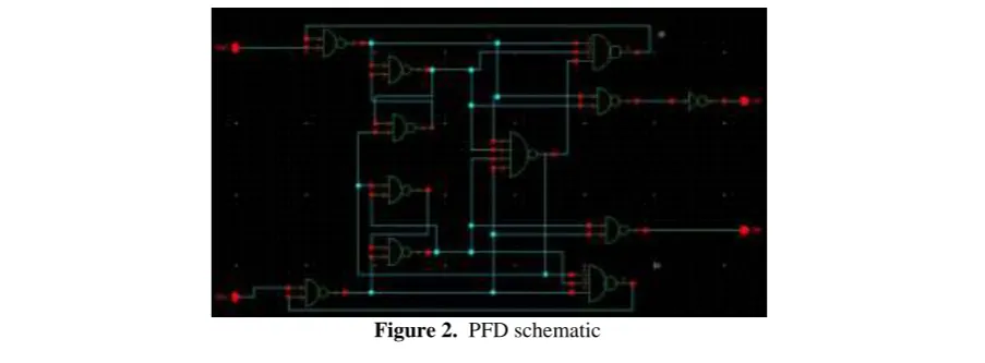
Phase detector is a module which produces output signals which is proportional to the phase of the input signals. The PD has namely two output signals UP and DOWN and the input signals are input reference signal and the output of the Programmable frequency divider. The architecture of the PD is depicted in Figure2.
3.2 Charge Pump
The Charge Pump can be modeled as transconductive device which convert the Phase difference of the input signals into the current. The circuit diagram of the charge Pump is depicted in Figure3.
Figure 3. Charge Pump Schematic 3.3 Loop filter
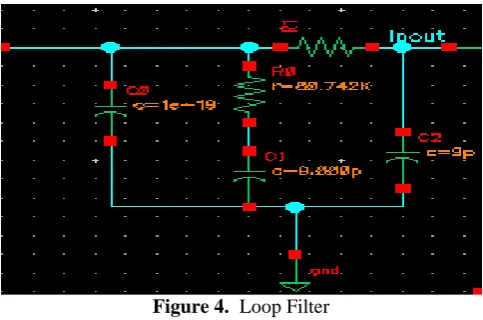
The function of the loop filter is to eliminate the unwanted high frequency signal and to integrate the DC voltage signal to the VCO. The Loop filter is designed using the following values in the table and by simulation of the eq.1.7 in the MATLAB environment and the values of the R and C are evaluated. The third order loop filter is depicted in Figure4.and the parameters considered while designing the loop filter are tabulated in the Table 1.
Figure 4. Loop Filter
Table 1.Parameters used in designing of the Loop Filter
3.4 Voltage Controlled Oscillator (VCO):
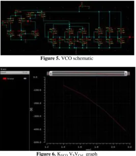
VCO works on the principle of the „Barkhausen Criteria‟. It states that “The frequency of oscillation at which sinusoidal oscillator operates is the frequency for which the total shift introduced, as the signal proceeds from the input terminals, through the amplifier and feedback network, and back again to the input, is precisely zero(or an integral multiple of 2*Π)(Or)Stated simply the condition A*β = -1 at ω= ωo, i.e. the magnitude of loop gain should be one and phase of loop gain should be unity ( the feedback network introduces 1800 phase shift, the other 1800 phase shift is provided by mixer ) is called Barkhausen criterion”. In VCO10 the frequency of oscillation is varied by the applied input DC voltage. When there is no input voltage, the output of the VCO will have a frequency called “free oscillation frequency”.It has an integratorfunction for the phase input signal. VCO which is designed in the present work is using the differential- ring oscillator. The gain of the VCO is denoted by KVCO and the gain of the KVCO designed is about 300MHz/V. The Figure5.depicts the schematic
Output frequency 800MHz
Input reference frequency 25MHz
Phase Margin 700
VCO gain 300 MHz/V
Charge Pump current 10uA
design of VCO which has 1V as controllable voltage and the output frequency is 600-800Mhz range and the gain of the VCO which is denoted by KVCO graph is depicted in Figure6.
Figure 5. VCO schematic
Figure 6. KVCO VSVCtrl graph 3.5 Programmable Frequency Divider
The Programmable frequency divider has two control inputs S1 & S0 to select the predefined customized frequencies. In this the frequency of the VCO is scaled down. The amount by which the frequency is scaled down is multiplied with the input reference frequency. The principle used here is
f out = N x fref (1.10)
Where N is the scale down factor in the frequency divider. When „S1S0‟ is „00‟, „01‟, „10‟ and „11‟ the frequencies are scaled down by 24,28,30 and 32 whereas the output frequency of the PLL obtained is 600,700,750 and 800MHz respectively. The schematic of the programmable frequency divider is depicted in the Figure 7.
Figure 7.Programmable frequency divider.
II.
Discussion
MHz. Similarly when „S1S0‟ is „01‟,‟10‟and „11‟ the output frequency of the PLL is 700,750 and 800MHz respectively. The Lock time and the power consumption for each frequency are summarized in Table 2.
Figure 8. Various outputs of PLL structure for 600MHz
Figure 9. Settling frequency of PLL structure for 600MHz
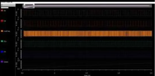
Figure 10. Various outputs of PLL structure for 700MHz
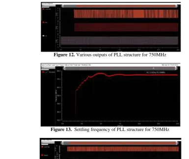
Figure 12. Various outputs of PLL structure for 750MHz
Figure 13. Settling frequency of PLL structure for 750MHz
Figure 14. Various outputs of PLL structure for 800MHz
Figure 15. Settling frequency of PLL structure for 800MHz Table 2. Lock time and Power consumption of the PLL for 600-800 Mhz
Selection input
Frequency in MHz
Lock time in µS Power
consumption(Watt)
00 600 9 12.5m
01 700 10 2.3
10 750 13 2.16
III.
Conclusion
In this paper, we have designed and simulated the programmable PLL structure has been done. The variation of the Lock time with the Frequency of oscillation is observed and also the power consumption at various frequencies is calculated. The Design and simulation of the whole structure is done in Cadence Virtuoso environment. The Proposed circuit is designed in 180nm, 3.3 V CMOS technology. The frequency range of the PLL is 600-800MHz and different precustomized frequencies in the range can be selected with S1 &S0inputs. The lock time of the circuit varied from 9 to 20 µS with variation of the frequency from 600 to 800MHz.
REFERENCES
[1]. Sumi Y, Syoubu K, Obote S, Fukui Y,PLL Frequency Synthesizer Using Multi- Phase Detector,Technical Meeting on Electronic Circuits, IEEE Japan. 1997 Jan 16 ,82(3),pp. 77-82.
[2]. Hagiwara M, Suzuki Y.Practical PLL frequency synthesizer,Sougou-denshiinc., 1995.
[3]. Sumi Y, Obote SNarai K, Tsuda K,Syoubu K, Fukui Y.Fast FrequencyAcquisition in the PLL Frequency SynthesizerSuppressing the Transient Response ofthe Second Order System, Technical Reportof IEICE, 1997, pp.69-76.
[4]. Sumi Y, Obote S, Tsuda K, Syoubu K, Fukui Y.A New Low Pass Filter for the Fast Frequency Acquisition of the PLL Frequency Synthesizer, 1 st Analog VLSI Workshop proceedings, 1997,pp. 115-20.
[5]. Ozawa T.Circuit Design of PLL Frequency Synthesizer, Sougoudensi Inc., 1994. [6]. Yanagisawa T. PLL Application Circuits,Sougoudensi Inc., 1995.
[7]. Adachi H, Kosugi H, Uwano T, Nakabe K.High-speed Frequency SwitchingSynthesizer Using Fractional N Phase Locked Loop, IEICE Trans.C, 1993,76(11), pp.445-52.
[8]. Razavi B,Design of Analog CMOS Integrated Circuits, 2ndedn. McGraw Hill Publisher, New Delhi, 2002.
[9]. MahdianH,Hashemi M, GhadimiAS,“Improvement in the Synchronization Process of the Voltage-Sourced Converters Connected to the Grid by PLL in Order to Detect and Block the Double Frequency Disturbance Term”,Indian Journal of Science and Technology. 2013 July, 6(7), pp.4940-52.