Sharifa et al. World Journal of Engineering Research and Technology
STUDY OF THE PROCESSES OF DEFECT FORMATION IN SILICON,
DOPED WITH COBALT
Sharifa B. Utamuradova*, Zafar O. Olimbekov
National University of Uzbekistan named after Mirzo Ulugbek, 100174, Tashkent, Republic
of Uzbekistan.
Article Received on 09/01/2018 Article Revised on 30/01/2018 Article Accepted on 20/02/2018
ABSTRACT
The processes of formation of deep centers in silicon mixed with
cobalt are investigated by means of methods of capacitive
spectroscopy. It was found that in n-Si, doped with cobalt formed four
deep levels with fixed energy of ionization: Ec-0.20 eV, Ec-0.33 eV, Ec
–0.45 eV and Ec –0.54 eV with capture cross section of charge carriers n=410-17 cm2, n =210-15 cm2, n =1.110-15 cm2 and n =1.510-15
cm2, respectively. It is shown that in the samples p-Si, doped with cobalt there is only one
level Еv +0.32 eV with charge carrier capture sections р=210-16 cm2, respectively.
KEYWORDS: Silicon, cobalt, deep level, level, doping, ionization energy, media capture cross-section.
INTRODUCTION
In recent years, to modify the properties of semiconductor materials, impurities of transition
elements are intensively used, the presence of which in the volume of monocrystalline silicon
affects the processes of defect formation.
Therefore, the study of the behavior of various impurities with deep levels in silicon, as well
as the study of the role of these impurities in the formation of electrophysical properties Si is
of great interest for solving important problems in this area. The behavior of a large number
of impurities with deep levels in silicon has been studied by many authors.[1-5]
World Journal of Engineering Research and Technology
WJERT
www.wjert.org
SJIF Impact Factor: 5.218*Corresponding Author Sharifa B. Utamuradova National University of
Uzbekistan named after
Mirzo Ulugbek, 100174,
Tashkent, Republic of
It is known that the least studied admixture among the impurities of transition elements in
silicon is cobalt and there is no definite opinion about the deep levels created by Co in Si and
about the behavior of its atoms in the silicon lattice.[2-4] In addition, these works do not take
into account the role of thermal and various uncontrolled defects in the processes of defect
formation in silicon doped with cobalt.
MATERIALS AND METHODS
In order to study the processes of formation of deep centers created by cobalt atoms in
silicon, we studied the properties of silicon doped by diffusion method using deep level
transient spectroscopy (DLTS) and photo capacitance. Diffusion of cobalt atoms in n- Si and
p-Si was carried out from the applied layer of metallic admixture in the temperature range
1000÷1250oC for 0.5÷30 hours, followed by cooling at different speeds (initial = 0.3÷40
Ohmcm). After cobalt diffusion, the resistivity of n-Si samples increased to 2104
Ohmscm, and in p-Si it did not change significantly. For carrying out capacitive
measurements were created Schottky barriers by evaporation in a vacuum of gold on n-Si and
antimony - on p-Si. As an Ohmic contact, Nickel was chemically deposited, sometimes
antimony or aluminum were sprayed.
DLTS spectra were measured in the modes of constant capacitance[6] and constant voltage,[7]
and the measurements of photo capacitance spectra were carried out according to the usual
methods described in.[8]
RESULTS AND DISCUSSION
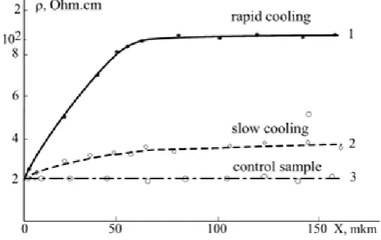
The study of the behavior of cobalt atoms introduced into silicon by diffusion showed that the
specific resistance distribution profile
in rapidly cooled samples Si<Co>, as well as otherimpurities of T-ions, is not described by the erfc function, but consists of two sections (Fig.1,
curve 1). Initially, there is a sharp increase in the resistivity
by 1.5-2 orders of magnitude toa depth of ~ 50 microns, then the value
is stabilized and a noticeable change
with a depthis not observed. It was found that the change in the resistivity depends on the cooling rate of
the samples after diffusion, in slowly cooled samples such a sharp increase in the resistivity
value was not found (Fig.1, curve 2). The values
in the control samples with depth did notFig. 1: Based on the resistivity distribution
depth in samples of Si<Со> (1, 2) and a control sample Si (3).Measurement of DLTS spectra has shown that after the introduction of the diffusion of an
impurity of cobalt in the samples n-Si (Fig.2, curves 1 and 2) deep levels with fixed
ionization energies are formed: Ec -0.20 eV (peak A), Ec -0.33 eV (peak C), Ec –0.45 eV
(peak C) and Ec –0.54 eV (peak D) with the capture cross section of charge carriers n=410 -17
cm2, n=210-15 cm2, n=1.110-15 cm2 and n=1.510-15 cm2, respectively. It is shown that
in the samples p-Si<Co> there is only one level in the lower half of the forbidden zone
Ev+0.32 eV with the capture cross section of charge carriers р=210-16 cm2, respectively.
The deep level of Ec-0.21 eV is also observed in heat-treated control samples (Fig.2, curve 3),
and here its concentration is much lower, than in n-Si<Co> (Fig.2, curves 1 and 2). This level
is probably a heat treatment defect.
Analysis of the results showed that the effectiveness of the education levels of Ec -0.33 eV, Ec
-0.45 eV and Ec -0.54 eV in n-Si<Co> and level Ev +0.32 eV in p-Si<> depends on
technological conditions of doping of silicon by admixture of cobalt (cooling rate after
diffusion υcooling). Comparison of curves 1 and 2 in Fig.2 shows that with a decrease in the
cooling rate after the diffusion υcooling, the concentrations of these levels fall significantly,
especially those of Ec -0.33 eV and Ec -0.45 eV.
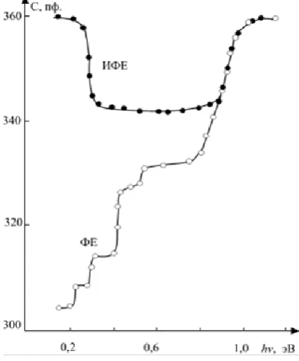
In samples n-Si diffusion doped with cobalt was also measured spectra of photo-capacitance.
Spectra photo-capacitance samples of n-Si doped with cоbalt discovered relaxation capacity
near h0.21 eV, h 0.33 eV, h 0.45 eV and h 0.54 eV (Fig. 3, curve 1).
Fig. 3: Spectra of photo capacitance (curve 1) and induced photo capacitance (curve 2) of n-Si<Co>samples.
Analysis of these spectra shows that the observed relaxation is due to the recharge of four
deep centers in the upper half of the forbidden zone: Ес -0.21 eV, Ес –0.33 eV, Ес –0.45 eV
and Ес -0.54 eV. Spectra photo-induced capacity of these samples there is one step close to
h 0.32 eV (Fig.3, curve 2) due to the level recharge in the lower half of the forbidden
zone: Еv +0.32 eV. The analysis of spectra DLTS and photo-capacitance shows that the
energy is thermal and the optical activation of the detected levels in samples n-Si<To>
CONCLUSIONS
Thus, we can conclude that diffusion doping of n-type silicon atoms of cobalt leads to the
formation of four deep levels with fixed energy of ionization: Ес -0.20 eV, Ес -0.33 eV, Ес –
0.45 eV and Ес –0.54 eV and a capture cross section of charge carriers n=410-17 cm2, n=210-15 cm2, n=1.110-15 cm2 and n=1.510-15 cm2, respectively. The introduction of
cobalt in the p-Si leads to the formation of one level in the lower half of the forbidden zone Еv +0.32 eV with sections of the capture of charge carriers р=210-16 cm2, respectively.
Analysis of the obtained results shows that the last three levels are associated with cobalt
atoms in silicon, and the level Ес -0.20 eV is probably a defect in heat treatment.
It is also found that the concentrations of the observed deep levels strongly depend on the
cooling rate of the post-diffusion υcooling: the higher υcooling, the greater the concentration
levels of Ес -0.33 eV, Ес -0.45 eV and Ес -0.54 eV.
REFERENCES
1. Korobko A. O., Lapchuk N. M. Shumskaya E. N. On the formation of the magnetic
ordering of crystalline silicon as a result of the implantation of cobalt ions. Bulletin of
BSU. Ser., 2005; 1(3): 48-53.
2. Isaev M.Sh., Norov S.G., Majidov A.D. a Study of the galvanomagnetic properties of the
surface layer of diffusion-doped Si. Electronic processing of materials, 2006; 5: 80-83.
3. Milns L. Impurities with deep levels in semiconductors. – M., Mir, 1977; 547.
4. E.M. Omel'yanovskii, V.I.Fistul. Impurities of transition metals in semiconductors. M.,
1983; 192.
5. Ravi K., Defects and impurities in semiconductor silicon. Per. from English. M., Mir,
1984; 471.
6. Lang D.V. Deep level transient spectroscopy a new method to characterize traps in
semiconductors. J. Appl. Phys, 1974; 45(7): 4. 3023-3032.
7. Miller G. L., Lang D.V., Kemmerling L. C. Capacitance transient spectroscopy. - Ann.
Rev. Mater. Sci., 1977; 7: 377-448.
8. Berman, L.S., Lebedev A.A. Capacitive spectroscopy of deep centers in semiconductors.