LETTER
Optimization of selective laser-induced
etching (SLE) for fabrication of 3D glass
microfluidic device with multi-layer micro
channels
Sungil Kim
1,2, Jeongtae Kim
1, Yeun‑Ho Joung
1, Sanghoon Ahn
2, Jiyeon Choi
2*and Chiwan Koo
1*Abstract
We present the selective laser‑induced etching (SLE) process and design guidelines for the fabrication of three‑ dimensional (3D) microfluidic channels in a glass. The SLE process consisting of laser direct patterning and wet chemi‑ cal etching uses different etch rates between the laser modified area and the unmodified area. The etch selectivity is an important factor for the processing speed and the fabrication resolution of the 3D structures. In order to obtain the maximum etching selectivity, we investigated the process window of the SLE process: the laser pulse energy, pulse repetition rate, and scan speed. When using potassium hydroxide (KOH) as a wet etchant, the maximum etch rate of the laser‑modified glass was obtained to be 166 μm/h, exhibiting the highest selectivity about 333 respect to the pristine glass. Based on the optimized process window, a 3D microfluidic channel branching to three multilayered channels was successfully fabricated in a 4 mm‑thick glass. In addition, appropriate design guidelines for preventing cracks in a glass and calibrating the position of the dimension of the hollow channels were studied.
Keywords: Glass micromachining, 3D laser micromachining, Selective laser‑induced etching, Subtractive manufacturing, 3D microchannel, Glass microfluidic device
© The Author(s) 2019. This article is distributed under the terms of the Creative Commons Attribution 4.0 International License (http://creat iveco mmons .org/licen ses/by/4.0/), which permits unrestricted use, distribution, and reproduction in any medium, provided you give appropriate credit to the original author(s) and the source, provide a link to the Creative Commons license, and indicate if changes were made.
Introduction
Over the past 30 years, researches on microfluidic devices using soft lithography have been conducted in a variety of industries including biology, chemistry, medicine, food, energy, and the environment [1–4]. The development of robust devices that can respond to various samples is essential for the expansion of the microfluidic devices’ capabilities. Typically, most microfluidic devices use polymer materials such as polydimethylsiloxane (PDMS) and polymethymethacrylate (PMMA). Nevertheless, glass can provide many advantages to the microfluidic
device research because of its excellent optical proper-ties, mechanical durability, chemical resistance, and easy electrode patterning [5–7]. However, in the fabrication of glass microfluidic devices, various microelectrome-chanical systems (MEMS) process steps such as mask-ing, etchmask-ing, drillmask-ing, and bonding are required and thus it takes more time and cost than soft lithography [8]. To overcome these disadvantages, we have studied a rapid fabrication process that can make an all-glass micro-fluidic device within an hour using ultrafast laser 3D direct writing [9, 10]. Ultrafast laser technology has been widely used in the microfabrication of various materials by taking the benefit of ultrashort laser pulses to mini-mize heat-affected zone (HAZ) which is critical for high precision, high speed, and high-quality manufacturing. Furthermore, the nonlinear absorption, which occurs in transparent media at very high laser intensity exceeding the order of ~ 1012 W/cm2, is the principle of 3D micro
Open Access
*Correspondence: [email protected]; [email protected] 1 Department of Electronics and Control Engineering, Hanbat National University, 125 Dongseodaero, Yuseong‑gu, Daejeon 34158, Republic of Korea
processing in glass [11]. Ultrashort laser pulses cause the absorption of photon only in the vicinity of a laser focus thus enable direct writing of 3D freeform patterns in a transparent material without a mask [12]. Therefore, ultrafast laser process has brought the opportunity of rapid and efficient glass microfabrication to microfluidics research [13–15].
Two-dimensional (2D) microfluidic channels of lab-on-a-chip and micro total analysis systems (µ-TAS) pro-vide simple and normal fluidic flow but have limited applications [16]. In the notion of three-dimensional (3D) channel structures enabling diverse applications upon intentionally designed complex flow characteris-tics, numerous 3D fabrication techniques such as multi-layer bonding and stereo lithography have been explored [17–19]. Recently, ultrafast laser based 2-photon polym-erization (TPP) has been demonstrated [20–22]. How-ever, TPP can only fabricate 3D microstructures in liquid phase polymer or glassy materials, thus the strength of final structures is not as stiff as made from solid phase materials. A 3D glass fabrication process called selective laser-induced etching (SLE), which was developed by Marcinkeviciu et al. in 2001, is a two-step hybrid process consisting of ultrafast laser beam irradiation and wet etch [23]. In the first step, a highly focused laser beam locally irradiates a glass and modifies its material properties to increase the chemical etch-ability. The laser-exposed area has different chemical and physical properties from pristine glass due to the nano-grating formation, vol-ume expansion, and internal stress [24–27]. In the sec-ond step, the modified area is selectively removed by wet etch. Therefore, the SLE process is basically a subtractive technique such as computer numerical control (CNC) or milling, not additive manufacturing such as a conven-tional 3D printer. It is similar to the stereo lithography for 3D structure fabrication using positive photoresist.
In the 3D structure fabrication, subtractive manufac-turing like SLE process has several advantages over addi-tive manufacturing. First, the tunneling process to etch a path inside material is very effective in fabricating micro-fluidic channels and drilling holes with a high aspect ratio. Second, it is possible to fabricate rigid 3D struc-tures maintaining intrinsic material properties because the subtractive manufacturing only removes unnecessary regions without adding other materials to the 3D struc-ture. Besides, subtractive manufacturing does not require additional work-pieces such as supports and bridges, unlike additive manufacturing. Third, it is a faster process than conventional glass microfabrication using photoli-thography, wet etching, and laser ablation. In particular, its’ direct writing nature offers any freeform patterns programmed in computer-aided design (CAD) without a mask, and the structure formed inside glass has high
durability because of no bonding process [28]. It also pro-vides the good surface quality below 1 μm surface rough-ness after wet etching [10, 15, 29].
However, sufficient investigations have not been con-ducted extensively yet to understand sophisticated vari-ation of process parameters of the SLE process to obtain high precision and dimension control for 3D microstruc-tures inside glass. Therefore, in this paper, we fabricated 3D glass microfluidic channels with SLE process optimi-zation based on the ultrafast laser. As a result, the micro-fluidic channel height resolution and channel expansion (dimension error) due to etching of the non-modified area were investigated.
Experiment setup
For the SLE experiments, an ultra-short pulsed laser (Satsuma HP2, Amplitude Systèmes, Pessac, France) with a central wavelength of 1030 nm and the maxi-mum output power of 20 W was used. The maximaxi-mum laser pulse energy was 40 μJ at the pulse repetition rate of 500 kHz and the pulse width variation was from 370 fs to 10 ps. The pulse repetition rate was variable up to 2000 kHz. For 3D fabrication machine, the laser ampli-fier was integrated with a 2-axis (XY) galvano scanner (DynAXIS, ScanLab, Puchheim, Germany) and an air bearing 3-axis(XYZ) servo motion stage with a controller (A3200, Aerotech, pittsburgh, USA). A focusing objective lens (NA = 0.4, model No. 378-867-5, Mitutoyo, Kawa-saki, JAPAN) was assembled with the galvano scanner for high scan speed. The focused laser beam size is esti-mated about 2 μm. The combined scan speed of the scan-ner and 3D stage is up to 200 mm/s and the field size is 100 mm × 100 mm. After laser modification process, the exposed glass substrate was etched using 8 mol potas-sium hydroxide (KOH) at 85 °C in an ultrasonic bath for uniform concentration control.
Optimization of the SLE process window for high selectivity
The SLE process window for high selectivity has been studied by various groups as the selectivity is the most important parameter that affects the fabrication resolu-tion and processing speed of 3D fabricaresolu-tion [24, 25, 30– 34]. As shown in the Eq. 1, the etch selectivity (S) can be obtained by dividing the laser-modified glass etch rate per hour (rm) and the pristine glass (unmodified) etch rate per hour (rn).
Processing parameters such as focusing geometry, polarization direction, laser pulse width, pulse rep-etition rate, pulse energy, and scan speed can affect the etch selectivity thus correct combination of process
(1)
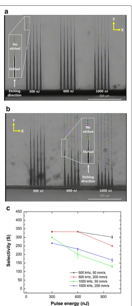
parameters need to be considered during the fabrication process. According to a prior study by Gottman et al., the pulse width of the picosecond regime provides a faster etch rate than femtosecond regime and the polarization direction of the laser leads a faster etch rate of the lin-early polarized light of the vector perpendicular to the direction of the laser beam. It has been reported by Her-mans et al. and Hnatovsky et al. [25–27, 29]. However, it is a challenging task to maintain vertical linear polari-zation in a laser scanning path for 3D structures [33]. Therefore, pulse energy, pulse repetition rate, and beam scan speed while using a fixed laser pulse width and x-axis polarization were dominant processing param-eters to obtain an optimized process window. 5 mm lines were patterned five times with 50 μm intervals in a 25 mm × 25 mm × 1 mm fused silica substrate (JMC glass, Ansan, Korea) as shown in Fig. 1a, b. The depth position was 0.5 mm, and two scan speeds at 50 mm/s and 200 mm/s were tested.
The modification threshold of the laser pulse energy was 300 nJ so that the pulse energy range was set up from 300 to 1000 nJ. The pulse repetition rate was 500 kHz and 1000 kHz. After wet etching in KOH, the substrate was rinsed with deionized (DI) water and dried using nitro-gen gas. Then the modified glass was observed through a transmitted illumination optical microscope. Figure 1a, b shows the formation of hollow channels in the glass after KOH etch. The one side of the channels was the start-ing point for the etch process and larger than the other side. The etch rate of the modified glass and the pristine glass in KOH was measured and the calculated selectiv-ity is summarized in Fig. 1c. The average etch rate of the unmodified glass is 0.5 μm/h. When using 300 nJ and 500 kHz, the average etch rate of the modified glass is about 166 μm/h and the selectivity is up to 333. In addi-tion, it seems that there is no significant difference in the selectivity in terms of the scan speed. However, a higher repetition rate decreases the selectivity since it generated high heat accumulation at the modified area and affected its etch rate.
How to design 3D structures using slice and hatch lines for laser direct writing
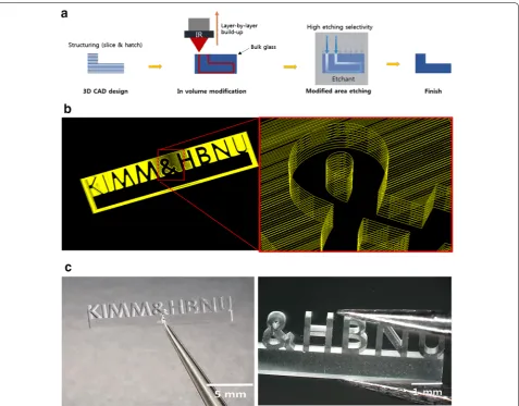
We optimized the structuring using slice and hatch lines and fabricated a 3D text structure as a demonstra-tion. Figure 2a shows a schematic of the whole process. A computer software for the laser 3D path creation in a bulk glass was developed to convert from a 3D CAD file consisting of hundreds to millions of vectors (STL format with polygon contour data) to horizontal slicing data (in the z-axis). After the conversion, the area to be removed is automatically filled with hatch lines having a set spac-ing (The first diagram in Fig. 2a). A fabrication controller
in the laser direct writing system computed the opti-mized laser beam path and conducted laser direct writ-ing in a glass sample (The second diagram in Fig. 2a). Then, the glass was immersed in KOH to etch the exte-rior of the 3D structure and to release the structure from the bulk glass (The third and fourth diagram in Fig. 2a). The test structure was designed in normal STL format and converted to slice and hatch data. The slice lines for the structuring are shown in Fig. 2b. Based on the data, the 3D structure was fabricated successfully (Fig. 2c). A 25 mm × 25 mm × 1 mm fused silica was used as a bulk substrate and the dimension of the 3D structure was 17 mm × 2.5 mm × 0.5 mm. The time for laser writing was about 2 h and the wet etch time in KOH was about 12 h.
The smaller slice and hatch line spacing induced a faster wet etch. However proper slice and hatch spac-ing should be selected, otherwise internal crackspac-ing was
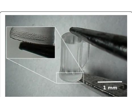
occurred during laser direct writing or wet etching pro-cess where the glass exposed expro-cessively. To investigate the effect of the small slice and hatch line spacing, several 3D hollow cubes with the width of 500 μm were fabri-cated using the combinations of the slice and hatch size of 10 or 20 μm. The pulse energy was 300 nJ for overall writing process. As shown in Fig. 3, the dense slice struc-turing using 10 μm spacing created microcracks at the corners of the cubes where the laser dose was slightly higher than interior of the cube due to the acceleration and deceleration of the scanner. On the other hand, if larger spacing of slice over 40 μm was used, some part of the glass was not etched as designed. Therefore, the slice and hatch sizes should be adjusted appropriately. Figure 4 shows the world smallest glass beer mug with the volume of 3 μL fabricated with the optimized slice and hatch line spacing of 20 μm, as far as our knowledge goes. It was fabricated with the pulse energy and the scan speed was
600 nJ and 200 mm/s respectively, and followed by 12 h etching. In addition, we could fabricate a few micrometer patterns on the bottom and side of the beer mug.
Design and fabrication of 3D glass multilayer microfluidic device
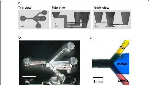
3D glass device having multilayer microfluidic structures was designed and fabricated in a 4 mm thick fused silica substrate, as shown in Fig. 5a. In the design, the maxi-mum length of the 3D microfluidic channel was 11 mm and the branching section to three microfluidic channels was at the center of the 3D channel. The branched micro-fluidic channels were located at different depths. In the initial experiment, to investigate the minimum resolu-tion for the height of the channel coming from the z-axis slice space, the height of each channel was designed to be 10 μm that is less than the slice spacing of 20 μm. Thus, only one slice was used for writing the channels. In a result, the fabricated channel height was about 35–38 μm and it was due to the length of the volume pixel (voxel) of the in-volume focused laser beam that was 35 μm in depth. Therefore, the length of a voxel determined the minimum resolution of the height of the channel. The
horizontal resolution is decided by the laser beam spot size (about 2 μm). The resolution can be improved by using an objective lens with higher magnification or using shorter laser wavelength by shrinking a voxel. In the next experiment, the height of the microfluidic chan-nels was designed to be 20 μm. The slice and hatch sizes for structuring in the laser software were all set to be 20 μm. The laser scan speed was set to 200 mm/s and the total scan time took 20 min for the designed 3D branch-ing microfluidic channel. Figure 5b shows the results of the fabricated 3D glass device having multilayer micro-fluidic structures after 5 days wet etch.
To check a blocked area or leakage inside multilayered microfluidic channels, three different color dyes were injected using a syringe pump, as shown in Fig. 5c. The device showed the independent flow of the dyes with-out any blocked area. However, the fabricated channel showed a tapered channel shape with a larger width at the starting point than the width in the middle of the nel. The etchant penetration into the microfluidic chan-nel starts from both ends of the chanchan-nel that are the inlet and the outlet. The etching at the starting point of the channel was accumulated for 5 days and the width and height of the channel region were increased compared to the design dimension. Therefore, the tapered microflu-idic channel shape is inevitable [24] and the offset should be considered when designing the channel dimension. In our result, the taper angle of the 11 mm long microfluidic channel was about 1.5°.
Conclusions and discussions
We introduced the selective laser-induced etching pro-cess using ultrafast laser direct writing and demon-strated the glass 3D micromachining that was highly challenged when using conventional fabrication meth-ods. We investigated that the etch rate is not pro-portionally increasing to laser dose, rather it is only maximized within narrow process windows in terms of scan speed, pulse energy, and proper hatch and slicing distance. First, the etch rates of the modified glass and the non-modified glass by ultrafast laser exposure were investigated and the etch selectivity of about 333 was obtained by optimizing the laser process conditions. Second, we optimized the structuring using slice and hatch lines. Overall, we found that the proper distribu-tion of voxels which leads to uniform modificadistribu-tion of glass is the key to successful SLE process. Lastly, a 3D glass microfluidic device with multilayered microfluidic channels was demonstrated successfully. The etching time for the 11 mm microfluidic channel structure was too long as about 5 days in KOH so that an optimized etch condition or a new etchant should be researched in future. We hope that the presented process helps to
Fig. 3 3D hollow cubes fabricated using different slice spacing. The left one used 10 μm slice and 10 μm hatch spacing. The middle one used 10 μm slice and 20 μm hatch spacing. The right one used 20 μm slice and 20 μm hatch spacing
design and fabricate not only glass parts including opti-cal components but also 3D microfluidic structures that develops a new dynamics fluid that conventional 2D microfluidic channels cannot provide.
Authors’ contributions
SK optimization of SLE process and writing this paper. JK design of 3D micro‑ fluidic channel and analyzing structure. Y‑HJ analysis of wet etching results. SA analysis of laser modified structures. JC improved 3D laser micromachining and reviewed this paper. CK supervised and reviewed this paper. All authors read and approved the final manuscript.
Funding
This work was supported by the Ministry of Trade Industry and Energy (MOTIE) under the Global Excellent Technology Innovation (Project No. 10053877) and National Research Foundation of Korea (NRF) funded by the Ministry of Sci‑ ence ICT and Future Planning (Project No. 2018R1C1B5044079).
Availability of data and materials Not applicable.
Competing interests
The authors declare that they have no competing interests.
Received: 27 July 2019 Accepted: 30 September 2019
References
1. Whitesides GM (2006) The origins and the future of microfluidics. Nature 442:368
2. Chin CD, Linder V, Sia SK (2012) Commercialization of microfluidic point‑of‑care diagnostic devices. Lab Chip 12:2118–2134
3. Sackmann EK, Fulton AL, Beebe DJ (2014) The present and future role of microfluidics in biomedical research. Nature 507:181–189 4. Serien D, Kawano H, Miyawaki A, Midorikawa K, Sugioka K (2018) Fem‑
tosecond laser direct write integration of multi‑protein patterns and 3D microstructures into 3D glass microfluidic devices. Appl Sci 8:147 5. Grover WH, Skelley AM, Liu CN, Lagally ET, Mathies RA (2003) Mono‑
lithic membrane valves and diaphragm pumps for practical large‑ scale integration into glass microfluidic devices. Sens Actuat B Chem 89:315–323
6. Grosse A, Grewe M, Fouckhardt H (2001) Deep wet etching of fused silica glass for hollow capillary optical leaky waveguides in microfluidic devices. J Micromech Microeng 11:257
7. Waldbaur A, Rapp H, Länge K, Rapp BE (2011) Let there be chip—towards rapid prototyping of microfluidic devices: one‑step manufacturing processes. Anal Methods 3:2681–2716
8. Iliescu C, Taylor H, Avram M, Miao J, Franssila S (2012) A practical guide for the fabrication of microfluidic devices using glass and silicon. Biomicro‑ fluidics 6:016505
9. Kim S, Kim J, Koo C, Joung YH, Choi J (2018) Rapid prototyping of 2D glass microfluidic devices based on femtosecond laser assisted selective etching process. Int Soc Optics Photonics 10522:105221V
10. Kim S, Kim J, Joung YH, Choi J, Koo C (2018) Bonding strength of a glass microfluidic device fabricated by femtosecond laser micromachining and direct welding. Micromachines 9:639
11. Watanabe W, Li Y, Itoh K (2016) Ultrafast laser micro‑processing of trans‑ parent material. Opt Laser Technol 78:52–61
12. Davis KM, Miura K, Sugimoto N, Hirao K (1996) Writing waveguides in glass with a femtosecond laser. Opt Lett 21:1729–1731
13. Sugioka K, Cheng Y (2014) Femtosecond laser three‑dimensional micro‑ and nanofabrication. Appl Phys Rev 1:041303
15. Meineke G, Hermans M, Klos J, Lenenbach A, Noll R (2016) A microfluidic opto‑caloric switch for sorting of particles by using 3D‑hydrodynamic focusing based on SLE fabrication capabilities. Lab Chip 16:820–828 16. Burshtein N, Chan ST, Toda‑Peters K, Shen AQ, Haward SJ (2019)
3D‑printed glass microfluidics for fluid dynamics and rheology. Curr Opin Colloid Interface Sci 43:1–14
17. Miri AK, Nieto D, Iglesias L, Goodarzi Hosseinabadi H, Maharjan S, Ruiz‑ Esparza GU, Shin SR (2018) Microfluidics‑enabled multimaterial maskless stereolithographic bioprinting. Adv Mater 30:1800242
18. Männel MJ, Selzer L, Bernhardt R, Thiele J (2019) Optimizing process parameters in commercial micro‑stereolithography for forming emul‑ sions and polymer microparticles in nonplanar microfluidic devices. Adv Mater Technol 4:1800408
19. Vanden DS, Lucklum F, Bunge F, Vellekoop M (2018) 3D printing solutions for microfluidic chip‑to‑world connections. Micromachines 9:71 20. Xu BB, Zhang YL, Xia H, Dong WF, Ding H, Sun HB (2013) Fabrication and
multifunction integration of microfluidic chips by femtosecond laser direct writing. Lab Chip 13:1677–1690
21. Weingarten C, Steenhusen S, Hermans M, Willenborg E, Schleifenbaum JH (2017) Laser polishing and 2PP structuring of inside microfluidic chan‑ nels in fused silica. Microfluid Nanofluid 21:165
22. Nava MM, Zandrini T, Cerullo G, Osellame R, Raimondi MT (2017) 3D stem cell niche engineering via two‑photon laser polymerization. Cell Cult 1612:53–266
23. Marcinkevičius A, Juodkazis S, Watanabe M, Miwa M, Matsuo S, Misawa H, Nishii J (2001) Femtosecond laser‑assisted three‑dimensional microfabri‑ cation in silica. Opt Lett 26:277–279
24. Bellouard Y, Said A, Dugan M, Bado P (2004) Fabrication of high‑aspect ratio, micro‑fluidic channels and tunnels using femtosecond laser pulses and chemical etching. Opt Express 12:2120–2129
25. Hermans M, Gottmann J, Riedel F (2014) Selective, laser‑induced etching of fused silica at high scan‑speeds using KOH. J Laser Micro/Nanoeng 9:126–131
26. Richter S, Heinrich M, Döring S, Tünnermann A, Nolte S, Peschel U (2012) Nanogratings in fused silica: formation, control, and applications. J Laser Appl 24:042008
27. Hnatovsky C, Taylor RS, Simova E, Bhardwaj VR, Rayner DM, Corkum PB (2005) Polarization‑selective etching in femtosecond laser‑assisted micro‑ fluidic channel fabrication in fused silica. Opt Lett 30:1867–1869 28. Sugioka K, Xu J, Wu D, Hanada Y, Wang Z, Cheng Y, Midorikawa K (2014)
Femtosecond laser 3D micromachining: a powerful tool for the fabrica‑ tion of microfluidic, optofluidic, and electrofluidic devices based on glass. Lab Chip 14:3447–3458
29. Gottmann J, Hermans M, Repiev N, Ortmann J (2017) Selective laser‑ induced etching of 3D precision quartz glass components for microflu‑ idic applications—up‑scaling of complexity and speed. Micromachines 8:110
30. Kiyama S, Matsuo S, Hashimoto S, Morihira Y (2009) Examination of etching agent and etching mechanism on femotosecond laser micro‑ fabrication of channels inside vitreous silica substrates. J Phys Chem C 113:11560–11566
31. LoTurco S, Osellame R, Ramponi R, Vishnubhatla KC (2013) Hybrid chemi‑ cal etching of femtosecond laser irradiated structures for engineered microfluidic devices. J Micromech Microeng 23:085002
32. Zhao M, Hu J, Jiang L, Zhang K, Liu P, Lu Y (2015) Controllable high‑ throughput high‑quality femtosecond laser‑enhanced chemical etching by temporal pulse shaping based on electron density control. Sci Rep 5:13202
33. Ross CA, MacLachlan DG, Choudhury D, Thomson RR (2018) Optimi‑ sation of ultrafast laser assisted etching in fused silica. Opt Express 26:24343–24356
34. Qi J, Wang Z, Xu J, Lin Z, Li X, Chu W, Cheng Y (2018) Femtosecond laser induced selective etching in fused silica: optimization of the inscrip‑ tion conditions with a high‑repetition‑rate laser source. Opt Express 26:29669–29678
Publisher’s Note