163304-9292-IJET-IJENS © August 2016 IJENS
Temperature Effect on the I-V Characteristics of the
MOSFET Transistor
Ouassila Benzaoui
1,2and Cherifa Azizi
31. Technology Department, Faculty of Technology, 20 August 1955 University, BP 26, Skikda 21000, Algeria. 2. Department of Physics, Faculty of Science, Mentouri Brothers University, Constantine 25000, Algeria
Email: o.benzaoui@gmail.com
3. Sciences Institute, Faculty of exact sciences, Larbi Ben M’hidi University, BP 358, Constantine Street, Oum El Bouaghi 04000, Algeria
Email: azizichhe@gmail.com
Abstract-- MOSFET Transistor occupies a fundamental place among all the components produced in micro-electronics. It was the subject of many studies and research to exploit its interesting and promising characteristics.
Owing to the fact that the semiconductors are very sensitive to the temperature, it is paramount to understand the phenomena that it involves. The aim of this contribution is the study of the temperature effect on the static I-V characteristics of the MOSFET.
The study enables us to calculate the drain current as a function of bias in both linear and saturated modes using a numerical simulation program; one could notice that the MOS transistor characteristics are very sensitive to the temperature. The inversion charge via the threshold voltage and the charge carrier mobility are the two principal influenced parameters. It was noted that the increase in the temperature induces a drop of the threshold voltage and carrier mobility. An immediate consequence of this reduction is the decrease in the drain current.
One can thus conclude that the temperature influences the performances of the device; the lower the temperature, the better is the reliability of the device under operation.
Index Term-- MOSFET; Temperature; Mobility; Performances.
I. INTRODUCTION
The MOS transistor is by far, the device the most encountered in the current production of semiconductor components, several acronyms are used in the literature to describe the MOS transistor (Metal Oxide Semiconductor) : MOSFET (MOS Field Effect Transistor), IGFET (Insulated Gate Field Effect Transistor) and MOST (Metal Oxide Semiconductor Transistor) [1].
Silicon technologies field-effect MOSFET transistors are very mature and offer components with very honorable performances because of the intrinsic physical properties at relatively low cost. This remains a major asset in the current context making it possible to fulfill the requirements of communication systems in terms of power.
The transistors are traditionally modulated by using the model of the equivalent diagram. However, this kind of models can only give one limited outline on the physical behavior of the component, which is why the physical models based on analytical description intervene, in terms of transport properties, geometrical and technological parameters of the transistor.
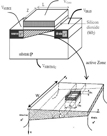
II. CALCULATION OF THE DRAIN CURRENT The figure (1) represents the elementary structure of the studied device; it is a N type MOSFET working in the static regime, its modeling requires several simplifications due to the difficulties imposed by the avalanche phenomena (substrate-drain junction) and source-drain drilling [2].
To calculate the drain current of the MOSFET one adopts the following assumptions [3]:
The insulator (SiO2) is ideal: absence of charge traps
in insulator and at the interface of the semiconductor. There is no difference in work between metal and the semiconductor.
The mobility of the carriers is constant in the inversion layer.
The doping of the channel is uniform in all the substrate.
The leakage current is negligible. W
Active Zone
N
N
e P
VGate
e
Silicon dioxide
e
activeZone
Approximation of the gradual charge: The transverse field Ex in the channel is more important than the
longitudinal field Ey.
Thus the variation of the drain current ID with the
drain-source voltage VD and the gate-source voltage VG is given by
the following general relation [4]:
32 32
2 1 2 2 2 3 2 2
2 ox D Fi Fi
S a D Fi D G ox D V C eN V V V L C Z
I (1)
However, this equation is rewritten differently, according to the operation regime of the transistor which depends primarily on the value of the drain voltage VD.
These regimes are: I. Linear regime
The drain voltage in this regime obeys to the following condition: VD≤VG-VT
Thus, the equation of drain current is rewritten [5]:
G T
Dox
D
V
V
V
L
C
Z
I
(2)With VT is the threshold voltage and Cox is the insulator
capacitance, both are given by:
a s Fi
ox FiT
eN
C
V
2
4
12 (3)d
C
oxox
(4)II. Saturation regime
The drain voltage is conditioned by: VD>VG
-VT
The drain current becomes [5]:
2 22
2
Dsat ox T G ox DsatV
L
C
Z
V
V
L
C
Z
I
(5)Where VDsat is the saturation voltage given by:
T G Fi G
Dsat
V
V
V
V
2
(6)III. RESULTS AND DISCUSSIONS
For the numerical calculation of the drain current versus bias voltage, one uses the data of transistors MOSFET1 (L=2.5m); MOSFET2 (L=1.5m) whose parameters are given in table 1.
Table I
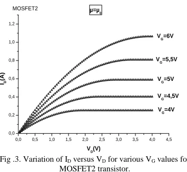
The figures (2) and (3) represent the variation of the drain current ID versus VD for various values of VG obtained
respectively for the MOSFET1(L=1.5m) and the MOSFET2 (L=2.5m), one notes that the drain current ID increases with
the voltage VD, then it saturates in the case of the MOSFET2
for a value for which the Space Charge Region (S.C.R) covers all the channel, contrary to the MOSFET1 which is saturated before the channel pinch. This is due to the fact that the length of the channel is short, which leads quickly to appreciable electric field values and consequently, fast saturation of the carriers velocity in the channel.
This means that the saturation of the drain current, in this case, is related to the saturation of the carriers velocity. It should be also noted that ID undergoes a reduction until its
annulment for a nonzero value of VG known as threshold
voltage.
IV. EFFECT OF VARIABLE MOBILITY
The mobility is a physical quantity defined as the proportionality factor between carriers velocity and the electric field, it depends in a complex way, on the nature and the frequency of the collisions and interactions undergone by the carriers during their displacement, it has a great influence on the current-voltage characteristics [5].
To show this dependence the two following laws were chosen:
MOSFET L
(m) D (A°)
Z (cm)
Na
(cm-3)
0
(cm2.s-1.v-1) ΦFi
(V) MOSFET1 1.5 1500 3.53 1016 277 0.35 MOSFET2 2.5 1000 2.81 1016 360 0.35
0,0 0,5 1,0 1,5 2,0 2,5 3,0 3,5 4,0 4,5 0,0 0,2 0,4 0,6 0,8 1,0 1,2 M0SFET1
VG=4V VG=4,5V VG=5V VG=5,5V VG=6V
ID
(A
)
VD(V)
µ=µ0
Fig. 2. Variation of ID versus VD for various VG values for
MOSFET1 transistor.
Fig .3. Variation of ID versus VD for various VG values for
MOSFET2 transistor.
0,0 0,5 1,0 1,5 2,0 2,5 3,0 3,5 4,0 4,5 0,0 0,2 0,4 0,6 0,8 1,0 1,2 V G=4V VG=4,5V V
G=5V V
G=5,5V VG=6V
MOSFET2 µ=µ0
ID
(A
)
163304-9292-IJET-IJENS © August 2016 IJENS
c T
G
V
E
E
V
1
0
1 (7) [4];
c T
G
V
E
E
V
1
1
0 2
(8) [1]0 the electron mobility under low field, and Ec (critical
field) are two parameters measured experimentally ([V-1] =1.5/d, Ec is about 5 10
4
v/cm).
In fact, the use of these expressions for MOSFET1 transistor, enables us to obtain the figures (4) and (5) on which one notes that the variations of the drain current are maximum in the case of 1. The current undergoes a reduction in the
saturation regime which is remarkable in the case of the mobility 2. This decrease is due to the fact that the
accumulation phenomenon of the charge carriers occurring in the channel is not taken into account.
V. EFFECT OF THE TEMPERATURE
The current characteristics of the MOSFET are strongly related to the temperature. However the majority of simulations suppose that the temperature of the component is constant. The room temperature (300 K) is usually taken as the component temperature.
The dependence of the carriers mobility on the temperature plays a fundamental role in the determination of the current. A simple law to model the variation of mobility with the temperature is the following one [6, 7, 8]:
kT
T
T
T
0
0 (9)
The variation the saturation speed with the temperature for the MOSFET is given by [9]:
600
T
exp
0.8
1
10
2.4
V
5
Sat (10)
The threshold voltage as a function of the temperature is given by [10, 11, 12]:
T
V
T
0
1
T
T
0
V
T
T
(11)Where T is the temperature of the network, T0 the
room temperature (300k), K a factor varying between 2.2 and 2.7 and γ is an empirical coefficient in the range from 2 to 3 mV/k.
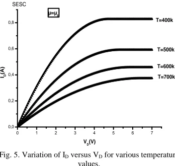
We studied the effect of the temperature on the static characteristics of the component, by numerical simulation using the mobility laws, the saturation speed and the threshold voltage. Calculation was carried out for MOSFET1transistor.
The figure (5) presents the variation of the drain current ID versus VD for various temperatures. It can be seen
that the drain current decreases with the temperature increase. This is an immediate consequence of the reduction of the mobility and the saturation speed as illustrated in figures (6) and (7) respectively.
0,0 0,5 1,0 1,5 2,0 2,5 3,0 3,5 4,0 0,0
5,0x10⁻⁹
1,0x10⁻⁸
1,5x10⁻⁸
2,0x10⁻⁸
2,5x10⁻⁸
VG=4V VG=4,5V VG=5V VG=5,5V VG=6V
MOSFET1
ID
(A
)
VD(V) µ=µ2
Fig. 5.Variation of ID versus VD for various VG
values obtained by using the expression of the mobility µ2.
0,0 0,5 1,0 1,5 2,0 2,5 3,0 3,5 4,0 0,0
5,0x10⁻⁹
1,0x10⁻⁸
1,5x10⁻⁸
2,0x10⁻⁸
2,5x10⁻⁸
VG=4V V
G=4,5V VG=5V VG=5,5V VG=6V
MOSFET1
ID
(A
)
VD(V) µ=µ1
Fig. 4. Variation of ID versus VD for various VG
values obtained by using the expression of the mobility µ1.
0 1 2 3 4 5 6 7
0,0 0,2 0,4 0,6 0,8
SESC
T=700k T=600k T=500k T=400k µ=µ0
ID
(A
)
VD(V)
Fig. 5. Variation of ID versus VD for various temperature
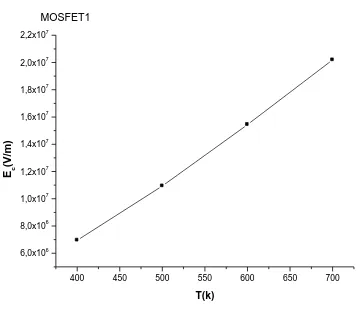
It should be noted that the rise in the temperature induces an intensive interaction between charge carriers and the optical phonons of the network. This leads to the decrease of the mobility and a limitation of the saturation speed of the carriers for a critical value of the lateral field EC. The latter
constantly increases with the temperature (fig.8).
The figures (9) and (10) show I-V characteristics in the case of variable nobilities µ1 and µ2.The same explanation as
in the case of constant mobility µ0 can be given, i.e. the drain
current is better at low temperature.
The variation of µ1 and µ2 nobilities versus the
temperature are presented on the figure (11), they decrease as the temperature increases
.
400 450 500 550 600 650 700 0,002
0,004 0,006 0,008 0,010 0,012 0,014
SESC
µ0
(m
2/V
s
)
T(k)
Fig. 6. Variation of mobility µ0 versus temperature.
400 450 500 550 600 650 700 6,5x10⁴
7,0x10⁴
7,5x10⁴
8,0x10⁴
8,5x10⁴
9,0x10⁴
9,5x10⁴
SESC
Vsat
(m
/S
)
T(k)
Fig. 7. Variation of saturation speed VSat versus the
temperature.
400 450 500 550 600 650 700 6,0x10⁶
8,0x10⁶
1,0x10⁷
1,2x10⁷
1,4x10⁷
1,6x10⁷
1,8x10⁷
2,0x10⁷
2,2x10⁷
MOSFET1
Ec
(V
/m
)
T(k)
Fig. 8. Variation of the saturation of the electric field Ec versus
the temperature.
0 1 2 3 4 5 6 7
0,0 2,0x10⁻⁹
4,0x10⁻⁹
6,0x10⁻⁹
8,0x10⁻⁹
1,0x10⁻⁸
1,2x10⁻⁸
1,4x10⁻⁸
1,6x10⁻⁸
1,8x10⁻⁸
SESC
µ=µ1
T=700k T=600k T=500k T=400k
ID
(A
)
VD(V)
Fig. 9. Variation of ID versus VD for various
temperatures values obtained by using the expression of the mobility µ1.
0 1 2 3 4 5 6 7
0,0 2,0x10⁻⁹
4,0x10⁻⁹
6,0x10⁻⁹
8,0x10⁻⁹
1,0x10⁻⁸
1,2x10⁻⁸
1,4x10⁻⁸
SESC
T=700k T=600k T=500k T=400k µ=µ
2
ID
(A
)
V
D(V)
Fig. 10. Variation of ID versus VD for various
temperatures values obtained by using the expression of the mobility µ2.
400 450 500 550 600 650 700 5,00E-011
1,00E-010 1,50E-010 2,00E-010 2,50E-010 3,00E-010
µ=µ1
µ=µ2
SESC
µ(m
2/V
s
)
T(k)
163304-9292-IJET-IJENS © August 2016 IJENS VI. CONCLUSION
In this paper, we developed a model allowing the description of the static electric operation of MOSFET in linear and saturated regimes, by taking into account the variation of mobility versus the electric field. The mobility law in the MOSFET which gives maximum variations of the drain current is given by the expression (7).
In addition the variation of the I-V characteristics of the component versus the temperature were obtained; the lower the temperature, the better is the reliability of the device under operation.
REFERENCES
[1] Skotnicki, T. : Transistor MOS et sa technologie de fabrication, Technique de l’ingénieur, traité Electronique, 1987.
[2] Muller, D. : Optimisation des potentialités d’un transistor LDMOS pour l’intégration d’amplificateur de puissance RF sur Silicium, Thèse de Doctorat, Université Limoge, 61-2006.
[3] SZE, S.M.: Physics of Semiconductor Devices, (2nd Edition). Taipei: John Wiley & sons, 1981.
[4] Mathieu, H. : Physique des semi-conducteurs et des composants électroniques, (2nd Edition). Dunod, Paris, 2001.
[5] Morancho, F. : Le transistor MOS de puissance à tranchées : Modélisation et Limites de Performance, Université Paul Sabatier, Toulouse, 1996, 96482.
[6] Arora, N.D., Hauser, J.R., Roulston, D.J.: Electron and Hole Mobilities in Silicon as a function of Concentration and Temperature, IEEE Transaction On Electron Devices, Vol. 30, N°6, p. 658-663, 1983.
[7] Klaassen, D.B.M.: A United Mobility Model for Device Simulation: II. Temperature Dependence of Carrier Mobility and Lifetime, Solid-State Electronics, Vol. 35, p. 961-967, 1992. [8] Dorkel, J.M., Leturq, P.: Carrier Mobilities in Silicon
Semi-Empirically Related to Temperature, Doping and Injection Level, Solid-State Electronics, Vol. 24, p. 821-824, 1981.
[9] Jacobini, C., Canali, C., Ottaviani, G., Alberigi Quaranta, A.: A Review of some Charge Transport Properties of Silicon, Solid-State Electronics, Vol. 20, p. 77-89, 1977.
[10] Arora, N.D.: MOSFET Models for VLSI Circuit Simulation- Theory and Practice, Editions Springer Verlag, 1993.
[11] Fatemizadeh, B., Silber, D.: Modeling of LDMOST and LIGBT Structures at High Temperatures, Proc. ISPSD and IC’s, Suisse, 1994.