International Journal of Computer Systems (ISSN: 2394-1065), Volume 04– Issue 06, June, 2017 Available at http://www.ijcsonline.com/
Design and Implementation of Memory Controller for Real Time Image
Acquisition using DDR2 SDRAM
Shweta A Mandaki, Dr H P Rajani
Department of Electronics and Communication, Visvesvaraya Technological University, Belagavi
Karnataka, India.
Abstract
The phenomenal development in the field of microelectronics has motivated the design engineer to integrate the complex systems of several million transistors in a single chip. There has been dynamic progression in the design of electronic systems, gadgets etc with evolving complexity and higher transaction speed. The evolution of fast and sophisticated state-of-art electronic system like processors and embedded systems, is fueled by the rapid development in the design and implementation of memory controllers. The design of DDR2 SDRAM controller can be done and implemented using FPGA technology to minimize the time to market and cost. The enhancement/improvement in the design of memory controller has led to achieve good support for memory and I/O devices.
This project work deals with capturing of real time images using camera and then storage and retrieval in efficient manner. The image is stored in JPEG format, transmitted over UART communication protocol to the FPGA and then it is written (stored) on chip memory of FPGA. Image data written in organized manner in FPGA will be further read and then transmitted to the VGA screen for the display of the real time image. The results are verified by real time display of the stored data and by using simulation and synthesis tools. This project deals with the designing of efficient memory controller for DDR2 SDRAM device. This project provides thorough explanation for the design and implementation of DDR2 SDRAM controller using Xilinx Design Suit 14.6 on FPGA board.
Keywords:DDR2 SDRAM, FPGA-Spartan 3A, Xilinx design suite 14.6, UART Communication Protocol, Webcam.
I. INTRODUCTION
There has been enormous progress in the area of integrated circuit design fueled by the phenomenal growth in the field of microelectronics. The evolution of memory devices has paved the way for memory device to operate at high speed, high bandwidth and low power. The advances in memory have led to the usage of memory devices in various multimedia applications such as live video transfer, real time image acquisition etc [1]. The memory devices are developed with ever increasing speed, bandwidth and latency [2]. The controller designed in this work aims interaction with memory and processor in order to gain more efficient operation.
Types of Memory Devices:
SDRAM (Synchronous Dynamic Random Access Memory):
“Synchronous” tells about the behavior of the DRAM type. SDRAM can stand for SDR SDRAM i.e. single data rate SDRAM where I/O, internal clock and bus width are same. Single data rate indicates that the memory can perform read/write operation once per clock cycle [3].
DDR SDRAM (Double Data Rate SDRAM):
The next generation of SDRAM is DDR which achieves higher bandwidth compared to SDRAM by transferring
data on both positive and negative edges of clock cycle (double pumping) without change in frequency of the clock. The transfer rate of DDR is twice that of SDRAM without any change in the internal clock rate. DDR SDRAM is the first generation SDRAM memory device. It has a data fetch rate with 2bit [3].
DDR2 SDRAM (Double Data Rate Two SDRAM): The advantage of using this memory is that, it operates the external data bus twice as fast as DDR SDRAM. The transfer rate of DDR2 is higher as compared to DDR with improved I/O signals. DDR2 allows higher bus speed and requires low power by running the internal clock at half the speed of data bus [3].
II. IMPLEMENTATION
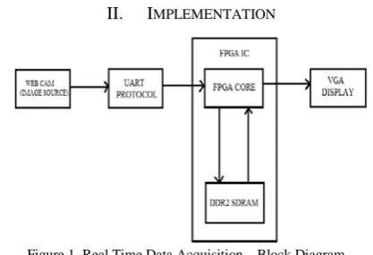
The real time data acquisition system is shown in the Figure 1. The camera captures real time images which is stored in JPEG format. The frame of image data is then transferred over UART communication protocol to the FPGA and then is written (stored) on the chip memory i.e. DDR2 SDRAM of FPGA. The data is retrieved (read) back from memory to the FPGA and further sent to VGA screen for real time display of image data.
A. Web Camera
Figure 2. Data capture through webcam
Webcam is a camera that is used to capture the image, it feeds a stream of real time image from one network to the other network. Webcam are installed in various electronic gadgets such mobile phones, laptops etc [4].
The data from the webcam is sent to FPGA through UART communication protocol. Further the image data is received by the memory controller present in FPGA.
B. UART Communication Protocol
UART stands for Universal Asynchronous Receiver and Transmitter. Purpose of UART is to transmit and receive the serial data.
Figure 3. UART transmission and reception module [5]
Here UART 1 is a transmitting UART and UART 2 is a receiving UART. Transmitting UART converts parallel data into serial form and transmits to receiving UART. Receiving UART then converts the serial data back to parallel form by the receiving device. Transmission and Reception of data occurs asynchronously meaning that no clock signal is used to synchronize the bits. Instead bits are synchronized on a transfer rate called baud rate [5].
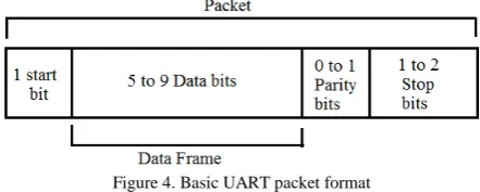
Figure 4. Basic UART packet format
UART packet format is shown in Figure 4. Each packet consists of 1 start bit, 5-9 data bits depending on the UART, 1 parity bit which is optional and 1 or 2 stop bits.
C. FPGA
FPGA is a widely used programmable logic which plays an important role in minimizing the time to market and cost. FPGAs consists of configurable programmable logic blocks (PLBs). Since FPGA reduces the time complexity and cost, they are increasingly used for standard prototype development.
D. VGA Controller
VGA is video display that is used to interface a frame of work with a screen to display data and images. VGA is referred to an array rather than an adapter, because it was implemented as a single chip from start. Its single chip implementation allowed VGA to be interfaced directly on a PC’s motherboard to reduce the difficulty in assembling. Since it only requires the timing crystals and the video memory [1].
VGA Principle:
Figure 5 below shows the scanning pattern for the VGA Controller.
• VGA is a standard video interface consisting of 640 Horizontal and 480 Vertical image components which are namely known as pixels. • The pixels are turned on and turned off
continuously to represent the image data.
• Once the values get updated in horizontal row, the pointer gets incremented to a new column and the procedure is repeated.
• VGA screen must be refreshed for every 60 seconds with a minimum frequency range of 60Hz to 120Hz.
Figure 5. Scanning pattern for VGA Controller [1] The eight basic color values for red green and blue are shown in the Table I.
E. Existing DDR2 SDRAM memory controller design
Figure presents the entire memory interface design for memory controller from user end to the DDR2 SDRAM. User interface connects the user design to memory controller through physical interface. Memory controller is mainly divided into two sections i.e. front end and back end of memory controller. Front end design provides a connection for reading and writing the data request by the user design and also provides a data transfer from user to the external memory. Back end design is employed at the physical interface end, which provides necessary signals and timings for clock, control, address, initialization, read and write of memory devices [2].
Figure 6. Existing Memory interface solution [2]
III. DESIGN DETAILS OF PROPOSED DDR2 SDRAM CONTROLLER FOR FPGA
The block diagram of DDR2 SDRAM designed in the work for real time image acquisition is shown in Figure 7.
Figure 7. Block diagram for Proposed DDR2 SDRAM Controller
CK and CK# are the differential clocks, where all the address and control signals are sampled on both positive and negative edge of CK and CK#. CKE is high throughout for read and write operation. ODT when registered high, enables the termination of internal resistance of DDR2 SDRAM. CS is registered low to activate a chip. RAS, CAS and WE define the command being entered. A0-A13 is 14 bit address, which provides a row address for active command and a column address for read/write command. BA0-BA1 is a bank address which defines which bank is active when read and write command is applied. DM is input mask signal for write data. The signal DQ provides a data to write or read depending upon the operation. DQS is a bidirectional data strobe bus with output as a read data and input with a write data.
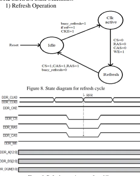
DDR2 SDRAM State Machines: 1)Refresh Operation
Figure 8. State diagram for refresh cycle
Figure 9. Refresh operation waveform [6]
issuing of the refresh command. Initially the state is in idle state i.e. reset. When busy_refresh=1, if ref==1, and CKE=1 then the state is in clk active state. When CS=0, RAS=0, CAS=0, WE=1 then the state is in Refresh state. When CS=1, CAS=1, RAS=1 and busy_refresh=0 the state is in idle state.
2)Precharge operation
Figure 10. State diagram for Precharge cycle
Figure11. Precharge operation waveform [6]
Precharge command deactivates the open row in a particular bank or open rows in all banks. Precharge command is used if there is no open row in a bank i.e. idle state. From the state diagram, initially the state is in idle state i.e. reset. When busy_precharge=1, if pre==1, and CKE=1 then the state is in clk active state. When CS=0, RAS=0, CAS=1, WE=0 then the state is in Precharge state. When CS=1, RAS=1, WE=1 and busy_precharge=0 the state is in idle state.
3)Bank active operation
Figure 12. State diagram for Bank active cycle
Figure 13. Bank active operation waveform [6]
The active command is used to open a row for a particular bank for subsequent access. Initially the state is in idle state i.e. reset. When busy_active=1, if active==1, and CKE=1 then the state is in clk active state. When CS=0, RAS=0, CAS=1, WE=1 then the state is in Active state. When CS=1, RAS=1, WE=1 and busy_active=0 the state is in idle state.
4)
Write operationFigure 14. State diagram for write cycle
Figure 15. Write operation waveform [6]
5)Read operation
Figure 16. State diagram for Read cycle
Figure 17. Read operation waveform [6]
The read command is used to initiate a read access to an active row. Initially the state is in idle state i.e. reset. When busy_read=1, if rd==1, and CKE=1 then the state is in clk active state. When CS=0, RAS=1, CAS=0, WE=1 then the state is in Read state. When CS=1, CAS=1, WE=0 and busy_read=0 the state is in idle state.
Finite State Machine for DD2 SDRAM:
The Complete state machine for DDR2 SDRAM is drawn by mathematical computation i.e. Finite state machines (FSM). The design flow for memory controller can be described as follows:
When ref==1, pre==1, active==1, wr==1, and rd == 1 the state is in clk active state. CS is registered low in order to active the chip. Specific Command signals are given in order to perform refresh, precharge, active, write and read operations. When CS is registered high, the chip gets deactivates and returns back to idle state.
Figure 18. FSM for DDR2 SDRAM memory
IV. RESULTS AND OBSERVATIONS
All the components required for Real Time Image Acquisition are discussed in section 2, as well as proposed memory controller. Various State diagrams and Finite state machine (FSM) was developed using DDR2 SDRAM Datasheets. The code was done in VHDL language using Xilinx Design suite 14.6
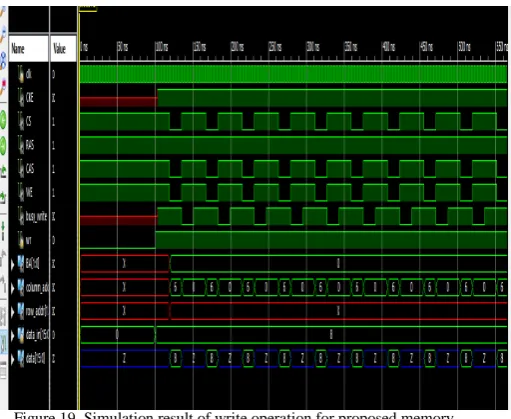
Figure 19 which is shown below represents the simulation result of write operation for proposed DDR2 memory controller, Figure 20 represents the simulation result for read operation of proposed memory controller starting from initialization, bank activation, address selection and desired write operation.
Figure 20. Simulation result of read operation for proposed memory controller
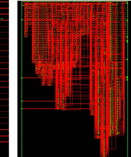
The RTL schematic allows to view the inputs and outputs of the system i.e the schematic for a designed netlist. Figure 21 depicts the RTL schematic for existing memory controller. Figure 22 depicts the RTL schematic for a proposed DDR2 SDRAM memory controller.
Figure 21. RTL Schematic for existing memory controller
Figure 22. RTL Schematic for proposed memory controller
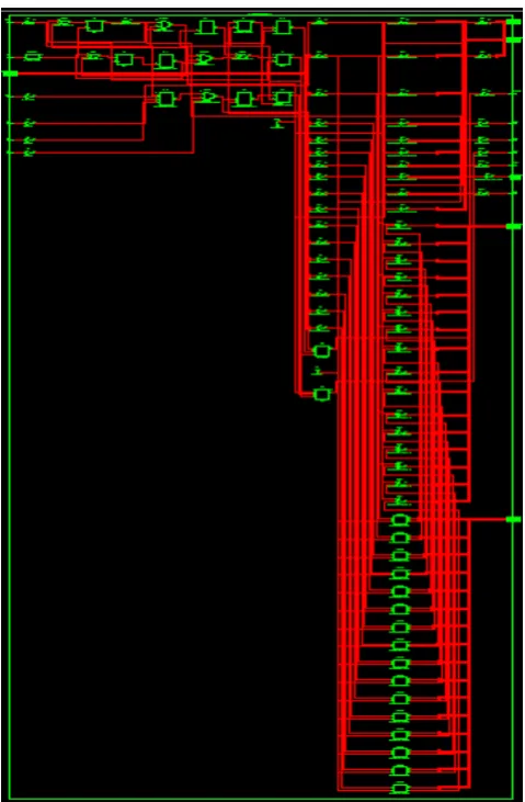
The technology schematic represnts the design in terms of I/O buffer and Look up table(LUT). Figure 23 represents the Technology schematic for existing memory controller. Figure 24 represents Technology schematic for proposed memory controller.
Figure 24. Technology Schematic for proposed memory controller
V. CONCLUSION
This work provides an effective design and implementation of memory controller for real time image acquisition on Xilinx Spartan 3A board. The proposed system is designed to operate at a frequency of 133MHz. Camera module is used to capture the image data and is sent to FPGA through UART. UART acts as a communication via between the Camera and FPGA. VGA display and ISE Simulator are used to verify the real time image data results. The memory controller is designed using Xilinx Design suit 14.6 to reduce power consumption and increase speed of operation. The project overviews the efficiency of DDR2 SDRAM memory controller and can be used in various applications.
REFERENCES
[1] Arun S. Tigadi, Veenabai A. L., and Hansraj Guhilot, “Design and implementation of memory controller for real time video display using ddr3 sdram,” International Research Journal of Engineering and Technology (IRJET), Volume: 03 Issue: 07, July-2016. [2] Arun S. Tigadi, Padmashree G., and Hansraj Guhilot, “Design and
implementation of memory controller for real time video acquisition using ddr3 sdram,” International Journal of Advanced Research in Electrical, Electronics and Instrumentation Engineering, Vol. 5, Issue 8, August 2016.
[3] Difference between SDRAM, DDR SDRAM, DDR2 SDRAM https://www.transcend-info.com/Support/FAQ-296.
[4] Webcam https://en.wikipedia.org/wiki/Webcam.
[5] http://www.circuitbasics.com/basics-uart-communication Basics of UART Communication – Circuit Basics.
![Figure 13. Bank active operation waveform [6]](https://thumb-us.123doks.com/thumbv2/123dok_us/1333549.1641766/4.595.311.536.78.223/figure-bank-active-operation-waveform.webp)