O
P T I C A L
P
R O X I M I T Y
D
E T E C T O R
Features
Applications
Description
The Si1102 is a high-performance (0–50 cm) active proximity detector. Because it operates on an absolute reflectance threshold principle, it avoids the ambiguity of motion-based proximity systems.
The Si1102 consists of a patented, high-EMI immunity, differential photodiode and a signal-processing IC with LED driver and high-gain optical receiver. Proximity detection is based on measurements of reflected light from a strobed, optically-isolated LED. The standard package for the Si1102 is an 8-pin ODFN.
Functional Block Diagram
High-performance proximitydetector with a sensing range of up to 50 cm
Single-pulse sensing mode for low system power
Adjustable detection threshold and strobe frequency
Proximity (PRX) status latch enables controlling devices to avoid missing a detection
High EMI immunity without shielded packaging
2 to 5.25 V power supply
Operating temperature range: –40 to +85 °C
Typical 10 µA current consumption and ultra-low power of 1 mA typical
Current driven (400 mA) or saturated LED driver output
Small outline: 3x3 mm (ODFN)
Proximity sensing Photo-interrupter Occupancy sensing Touchless switch Object detection Handsets Intrusion/tamper detection IR Signal processing PRX SREN TXO FR LED Drive Shutdown control Oscillator VDD Infrared emitter Product Case Hi-Lo Threshold Output
Reflectance-Based Proximity Detection
U.S. Patent 5,864,591 U.S. Patent 6,198,118 U.S. Patent 7,486,386 Other patents pending
Pin Assignments FR VSS TXO TXGD SREN VDD PRX DNC 1 2 3 4 8 7 6 5 Si1102 ODFN
T
A B L E
O F
C
O N T E N TS
Section
Page
1. Electrical Specifications . . . 4
2. Typical Application Schematic . . . 6
3. Application Information . . . 7
3.1. Theory of Operation . . . 7
3.2. Choice of LED and LED Current . . . 8
3.3. Power-Supply Transients . . . .8
3.4. Mechanical and Optical Implementation . . . 8
3.5. Typical Characteristics . . . 10
4. Pin Descriptions—Si1102 . . . 12
5. Ordering Guide . . . 13
6. Photodiode Center . . . 13
7. Package Outline (8-Pin ODFN) . . . 14
Document Change List . . . 15
1. Electrical Specifications
Table 1. Absolute Maximum Ratings
Parameter Conditions Min Typ Max Units
Supply Voltage –0.3 — 5.5 V
Operating Temperature –55 — 85 °C
Storage Temperature –65 — 85 °C
Voltage on TXO with respect to GND
–0.3 — 5.5 V
Voltage on all other Pins with respect to GND
–0.3 — VDD + 0.3 V
Maximum total current through TXO (TXO Active)
— — 500 mA
Maximum Total Current through TXGD and VSS
— — 600 mA
Maximum Total Current through all other Pins
— — 100 mA
ESD Rating Human body model — — 2 kV
Table 2. Recommended Operating Conditions
Parameter Symbol Conditions/Notes Min Typ Max Units
Supply Voltage VDD –40 to +85 °C, VDD to VSS 2.2 3.3 5.25 V
Operating Temperature –40 25 85 °C
SREN High Threshold VIH VDD – 0.6 — — V
SREN Low Threshold VIL — — 0.6 V
Active TXO Voltage1 — — 1.0 V
Peak-to-Peak Power Supply Noise Rejection
VDD= 3.3 V, 1 kHz–10 MHz no spurious PRX or less than 20%
reduction in range
— — 50 mVPP
on VDD
DC Ambient light Edc VDD= 3.3 V — 1 100 klux
LED Emission Wavelength2 600 850 950 nm
Notes:
1. Minimum R1 resistance should be calculated based on LED forward voltage, maximum LED current, LED voltage rail used, and maximum active TXO voltage.
2. When using LEDs near the min and max wavelength limits, higher radiant intensities may be needed to achieve the system's proximity sensing performance goals.
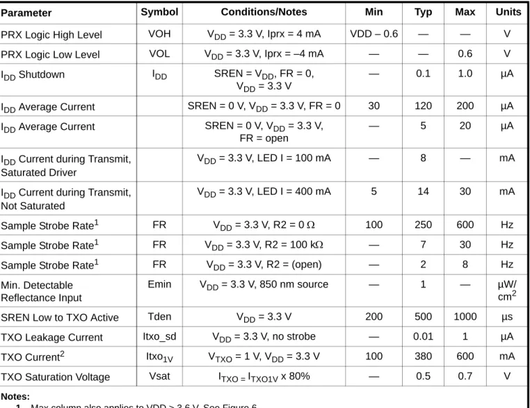
Table 3. Electrical Characteristics
Parameter Symbol Conditions/Notes Min Typ Max Units
PRX Logic High Level VOH VDD= 3.3 V, Iprx = 4 mA VDD – 0.6 — — V
PRX Logic Low Level VOL VDD= 3.3 V, Iprx = –4 mA — — 0.6 V
IDD Shutdown IDD SREN = VDD, FR = 0,
VDD= 3.3 V
— 0.1 1.0 µA
IDD Average Current SREN = 0 V, VDD= 3.3 V, FR = 0 30 120 200 µA
IDD Average Current SREN = 0 V, VDD= 3.3 V,
FR = open
— 5 20 µA
IDD Current during Transmit, Saturated Driver
VDD= 3.3 V, LED I = 100 mA — 8 — mA
IDD Current during Transmit, Not Saturated
VDD= 3.3 V, LED I = 400 mA 5 14 30 mA
Sample Strobe Rate1 FR VDD= 3.3 V, R2 = 0 100 250 600 Hz
Sample Strobe Rate1 FR VDD= 3.3 V, R2 = 100 k — 7 30 Hz
Sample Strobe Rate1 FR VDD= 3.3 V, R2 = (open) — 2 8 Hz
Min. Detectable Reflectance Input
Emin VDD= 3.3 V, 850 nm source — 1 — µW/
cm2
SREN Low to TXO Active Tden VDD= 3.3 V 200 500 1000 µs
TXO Leakage Current Itxo_sd VDD= 3.3 V, no strobe — 0.01 1 µA
TXO Current2 Itxo1V VTXO= 1 V, VDD= 3.3 V 100 380 600 mA
TXO Saturation Voltage Vsat ITXO =ITXO1V x 80% — 0.5 0.7 V
Notes:
1. Max column also applies to VDD > 3.6 V. See Figure 6.
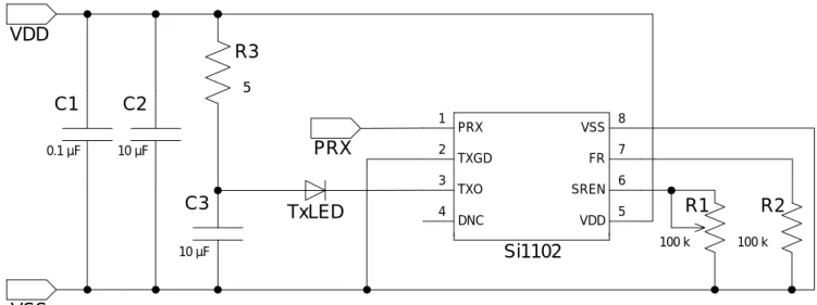
2. Typical Application Schematic
Figure 1. Application Example of the Proximity Sensor Using a Single Supply
PRX
PRX 1 TXGD 2 3 TXO 4 DNC VSS FR SREN VDD 8 7 6 5Si1102
VDD
VSS
C1
C2
C3
R3
TxLED
R1
R2
0.1 µF 10 µF 10 µF 5 100 k 100 kNote: R1 resistance should be factory-adjustable to achieve a consistent proximity object detection threshold across
3. Application Information
3.1. Theory of Operation
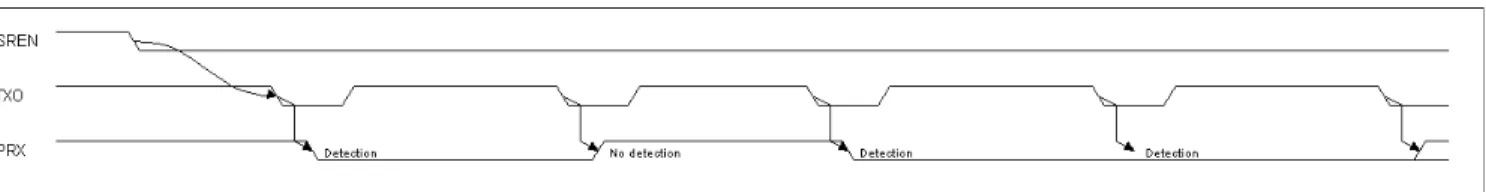
The Si1102 is an active optical reflectance proximity detector with a simple on/off digital output whose state is based upon the comparison of reflected light against a set threshold. An LED sends light pulses whose reflections reach a photodiode and are processed by the Si1102’s analog circuitry. If the reflected light is above the detection threshold, the Si1102 asserts the active-low PRX output to indicate proximity. This output can be used as a control signal to activate other devices or as an interrupt signal for microcontrollers. Note that when the proximity of an object nears the pre-set threshold, it is normal for the PRX pin to alternate between the on and off states. The microcontroller can take the time average of PRX (assigning 1 as “no detect” and 0 as “detect”) and then compare the average to 0.5 to achieve a sharper in-proximity or out-of-proximity decision.
To achieve maximum performance, high optical isolation is required between two light ports, one for the transmit LED and the other for the Si1102. The Si1102 light port should be infrared-transmissive, blocking visible light wavelengths for best performance. This dual-port active reflection proximity detector has significant advantages over single-port, motion-based infrared systems, which are good only for triggered events. Motion detection only identifies proximate moving objects and is ambiguous about stationary objects. The Si1102 allows in- or out-of-proximity detection, reliably determining if an object has left the out-of-proximity field or is still in the field even when not moving.
An example of a proximity detection application is controlling the display and speaker of a cellular telephone. In this type of application, the cell phone turns off the power-consuming display and disables the loudspeaker when the device is next to the ear, then reenables the display (and, optionally, the loudspeaker) when the phone moves more than a few inches away from the ear.
For small objects, the drop in reflectance is as much as the fourth power of the distance; this means that there is less range ambiguity than with passive motion-based devices. For example, a sixteen-fold change in an object's reflectance means only a fifty-percent drop in detection range.
The Si1102 proximity detector is designed to operate with a minimal number of external components. Figure 1 shows a circuit example using a single 3.3 V power supply. The potentiometer, R1, is used to set the proximity detection threshold. The Si1102 periodically detects proximity at a rate that can be programmed by a single resistor (R2). The part is powered down between measurements. The resulting average current, including that of the LED, can be as low as a few microamperes, which is well below a typical lithium battery's self-discharge current of 10 µA, thus ensuring the battery's typical life of 10 years.
When enabled (SREN driven low by a microcontroller or R1 pull-down potentiometer exists), the Si1102 powers up, then pulses the output of the LED driver. Light reflected from a proximate object is detected by the receiver, and, if it exceeds a threshold set by the potentiometer at the SREN pin, the proximity status is latched to the active-low PRX output pin. The output is updated once per cycle. The cycle time is controlled through the optional R2 resistor.
Although the thresholds are normally set using a potentiometer for R1 (or R2), it is possible to digitally control various resistance values by using MCU GPIO pins to switch-in different value resistors (or parallel combinations of resistors). To activate the chosen resistor(s), the GPIO pin is held low, creating a pull-down resistor. For the unwanted resistors, those specific MCU pins are kept tri-stated, rendering those resistors floating.
3.2. Choice of LED and LED Current
In order to maximize detection distance, the use of an infrared LED is recommended. However, red (visible) LEDs are viable in applications where a visible flashing LED may be useful and a shorter detection range is acceptable. White LEDs have slow response and do not match the Si1102’s spectral response well; they are, therefore, not recommended.
To maximize proximity detection distance, an LED with a peak current handling of 400 mA is recommended. With careful system design, the duty cycle can be made low, enabling most LEDs to handle this peak current while keeping the LED's average current draw on the order of a few microamperes.
Another consideration when choosing an LED is the LED's half-angle. An LED with a narrow half-angle focuses the available infrared light using a narrower beam. When the concentrated infrared light encounters an object, the reflection is much brighter. Detection of human-size objects one meter away can be achieved when choosing an LED with a narrower half-angle and coupling it with an infrared filter on the enclosure.
3.3. Power-Supply Transients
Despite the Si1102's extreme sensitivity, it has good immunity from power-supply ripple, which should be kept below 50 mVpp for optimum performance. Power-supply transients (at the given amplitude, frequency, and phase) can cause either spurious detections or a reduction in sensitivity if they occur at any time within the 300 µs prior to the LED being turned on. Supply transients occurring after the LED has been turned off have no effect since the proximity state is latched until the next cycle. The Si1102 itself produces sharp current transients on its VDD pin, and, for this reason, must also have a low-impedance capacitor on its supply pins. Current transients at the Si1102 supply can be up to 20 mA.
The typical LED current peak of 400 mA can induce supply transients well over 50 mVpp, but those transients are easy to decouple with a simple R-C filter because the duty-cycle-averaged LED current is quite low. The TXO output can be allowed to saturate without problem. Only the first 10 µs of the LED turn-on time are critical to the detection range; this further lessens the need for large reservoir capacitors on the LED supply. In most applications, 10 µF is adequate. If the LED is powered directly from a battery or limited-current source, it is desirable to minimize the load peak current by adding a resistor in series with the LED’s supply capacitor.
If a regulated supply is available, the Si1102 should be connected to the regulator’s output and the LED to the unregulated voltage, provided it is less than 7 V. There is no power-sequencing requirement between VDD and the LED supply.
3.4. Mechanical and Optical Implementation
It is important to have an optical barrier between the LED and the Si1102. The reflection from objects to be detected can be very weak since, for small objects within the LED's emission angle, the amplitude of the reflected signal decreases in proportion with the fourth power of the distance. The receiver can detect a signal with an irradiance of 1 µW/cm2. An efficient LED typically can drive to a radiant intensity of 100 mW/sr. Hypothetically, if this LED were to couple its light directly into the receiver, the receiver would be unable to detect any 1 µW/cm2 signal since the 100 mW/cm2 leakage would saturate the receiver. Therefore, to detect the 1 µW/cm2 signal, the internal optical coupling (e.g. internal reflection) from the LED to the receiver must be minimized to the same order of magnitude (decrease by 105) as the signal the receiver is attempting to detect. As it is also possible for some LEDs to drive a radiant intensity of 400 mW/sr, it is good practice to optically decouple the LED from the source by a factor of 106.
If an existing enclosure is being reused and does not have dedicated openings for the LED and the Si1102, the proximity detector may still work if the optical loss factor through improvised windows (e.g. nearby microphone or fan holes) or semi-opaque material is not more than 90% in each direction. In addition, the internal reflection from an encased device's PMMA (acrylic glass) window (common in cellular telephones, PDAs, etc.) must be reduced through careful component placement. To reduce the optical coupling from the LED to the Si1102 receiver, the distance between the LED and the Si1102 should be maximized, and the distance between both components (LED and Si1102) to the PMMA window should be minimized. The detector can also work without a dedicated window if a semi-opaque plastic case is used.
For applications where R1 resistance values are small, the proximity range can vary as a function of the ambient IR condition. A product cover, which limits the visible light intensity, is helpful in reducing this range variation. It is recommended that the Si1102 be evaluated and tested in-product under the various light conditions it will encounter under normal product usage. Setting the potentiometer R1 = 0 is not recommended unless the ambient light condition is known and relatively constant.
At any given R1 threshold setting, there are many factors that determine the precise distance that the Si1102 reports. These factors include object reflectivity, object size, ambient light type and ambient light intensity. When used in applications where the ambient light is variable, it is recommended the Si1102 optical window be IR transmissive but visible light opaque.
Figure 3. Proximity Detection Distance vs. R1 (SFH4650 IR LED 850 nm/40 mW)*
*Note: Detection range measured using Kodak Gray cards (18% reflectance), no IR filter under dark ambient conditions (<1 lx).
Table 4. Summary of External Component Values and Operating Conditions
R1 R2 Strobe Frequency Distance1 IDD Average Current Consumption2
50 k 0 250 Hz 12 to 22 cm 100 µA
50 k Open 2.0 Hz 12 to 22 cm 5 µA
15 k 0 250 Hz 40 to 50 cm 100 µA
30 k 0 250 Hz 17 to 33 cm 100 µA
Notes:
1. Distance measured with SFH4650 IR LED, with an IR filter, targeting an 18% gray card, 300 lux (Incandescent or CFL)
2. Average current consumption at VDD = 3.3 V, 25 °C and dark ambient conditions (<100 lx).
Detection Distance
5
10
15
20
25
30
35
40
45
50
10
20
30
40
50
60
70
80
90
100
R1(kohm) D et ect ion D ist ance ( cm )3.5. Typical Characteristics
Figure 4. Cycle Period vs. R2
(R1 = 5.1 k
, Vtxo = 1 V)
Figure 5. Idle Supply Current vs. R1
(R2 = 0 k
, Vtxo = 1 V)
Figure 6. Cycle Period vs. V
DDFigure 7. Idle Supply Current vs. R2
(R1 = 5.1 k
, Vtxo = 1 V)
Figure 8. Idle Supply Current vs V
DD(R1 = 5.1 k
, R2 = 0
, Vtxo = 1 V)
Cycle Period vs R1 1 10 100 1000 0 20 40 60 80 100 R1 (Kohm) C ycl e P e ri o d (m s) 5.0 volts 3.3 volts 2.0 volts Idd Idle 60 80 100 120 140 160 180 0 20 40 60 80 100 R1 (Kohm) Id d Id le 5.0 volts 3.3 volts 2.0 volts 0 10 20 30 40 50 60 70 80 90 100 110 120 130 140 150 160 2 2.5 3 3.5 4 4.5 Cycl e Time (ms) VDD (V) Cycle Time vs VDD R2=100K R2=75K R2=50K R2=30K R2=20K R2=10K R2=4.7KSupply Current Idle
1 10 100 1000 0 20 40 60 80 100 R2 (Kohm) Cu rr e n t ( u A) 5.0 volts 3.3 volts 2.0 volts Idd Idle vs VDD 50 55 60 65 70 75 80 85 90 95 2 2.5 3 3.5 4 4.5 VDD (V) Id d ( uA )
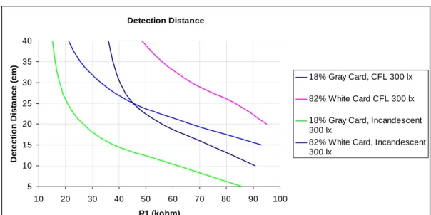
Figure 9. Proximity Detection Distance vs. Target Reflectivity (with IR Filter)
Figure 10. Proximity Detection Distance vs. Ambient Light (with IR Filter)
Detection Distance 5 10 15 20 25 30 35 40 10 20 30 40 50 60 70 80 90 100 R1 (kohm) D e tect ion D ist anc e ( c m ) 18% Gray Card, CFL 300 lx 82% White Card CFL 300 lx 18% Gray Card, Incandescent 300 lx
82% White Card, Incandescent 300 lx Detection Distance 5 10 15 20 25 30 35 40 20 30 40 50 60 70 80 90 100 R1 (kohm) D et ect ion D is tance ( cm ) 18% Gray Card, 0 lx 18% Gray Card, CFL 300 lx 18% Gray Card, CFL 1000 lx
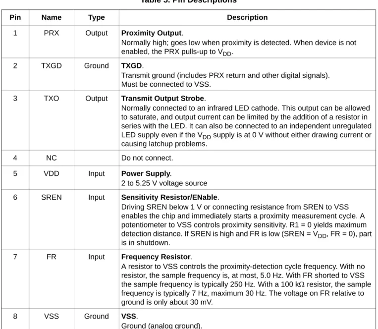
4. Pin Descriptions—Si1102
Figure 11. Pin Configuration
Table 5. Pin Descriptions
Pin Name Type Description
1 PRX Output Proximity Output.
Normally high; goes low when proximity is detected. When device is not enabled, the PRX pulls-up to VDD.
2 TXGD Ground TXGD.
Transmit ground (includes PRX return and other digital signals). Must be connected to VSS.
3 TXO Output Transmit Output Strobe.
Normally connected to an infrared LED cathode. This output can be allowed to saturate, and output current can be limited by the addition of a resistor in series with the LED. It can also be connected to an independent unregulated LED supply even if the VDD supply is at 0 V without either drawing current or causing latchup problems.
4 NC Do not connect.
5 VDD Input Power Supply.
2 to 5.25 V voltage source
6 SREN Input Sensitivity Resistor/ENable.
Driving SREN below 1 V or connecting resistance from SREN to VSS enables the chip and immediately starts a proximity measurement cycle. A potentiometer to VSS controls proximity sensitivity. R1 = 0 yields maximum detection distance. If SREN is high and FR is low (SREN = VDD, FR = 0), part is in shutdown.
7 FR Input Frequency Resistor.
A resistor to VSS controls the proximity-detection cycle frequency. With no resistor, the sample frequency is, at most, 5.0 Hz. With FR shorted to VSS the sample frequency is typically 250 Hz. With a 100 k resistor, the sample frequency is typically 7 Hz, maximum 30 Hz. The voltage on FR relative to ground is only about 30 mV.
8 VSS Ground VSS.
Ground (analog ground).
PRX TXGD TXO NC VSS FR SREN VDD 1 2 3 4 8 7 6 5
5. Ordering Guide
6. Photodiode Center
Figure 12. Photodiode Center
Part Ordering # Temperature Package
Si1102-A-GM –40 to +85 °C 3x3 mm ODFN8
1.5
7. Package Outline (8-Pin ODFN)
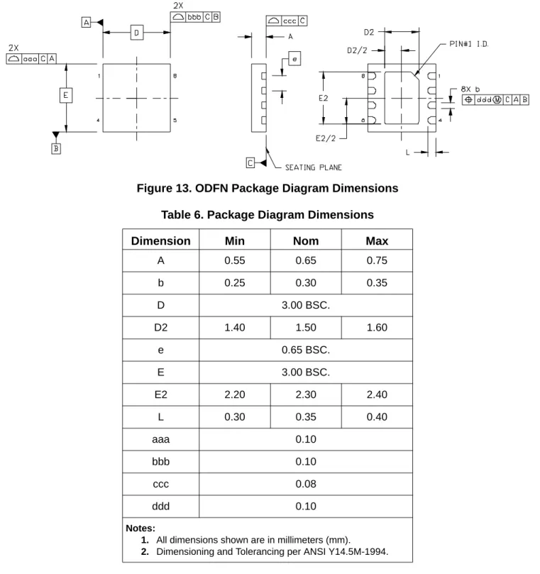
Figure 13 illustrates the package details for the Si1102 ODFN package. Table 6 lists the values for the dimensions shown in the illustration.
Figure 13. ODFN Package Diagram Dimensions
Table 6. Package Diagram Dimensions
Dimension
Min
Nom
Max
A 0.55 0.65 0.75 b 0.25 0.30 0.35 D 3.00 BSC. D2 1.40 1.50 1.60 e 0.65 BSC. E 3.00 BSC. E2 2.20 2.30 2.40 L 0.30 0.35 0.40 aaa 0.10 bbb 0.10 ccc 0.08 ddd 0.10 Notes:
1. All dimensions shown are in millimeters (mm).
DOCUMENT CHANGE LIST
Revision 0.6 to Revision 0.7
Revised outline drawing for 3x3 ODFN.
Adjusted pin width to match true scale
Tightened tolerance on body dimensions
Revision 0.7 to Revision 0.8
Updated Tables 1, 2, 3, 4, and 5.
Updated Figures 1, 2, 3, 5, 11, and 12.
Revision 0.8 to Revision 1.0
Updated Table 2, Table 3, and Table 5
Updated Figure 1 and Figure 6.
Updated Section 3.4 concerning usage of small R1 values.
Connected. Energy-Friendly. Products www.silabs.com/products Quality www.silabs.com/quality
Support and Community
community.silabs.com
Disclaimer
Silicon Laboratories intends to provide customers with the latest, accurate, and in-depth documentation of all peripherals and modules available for system and software implementers using or intending to use the Silicon Laboratories products. Characterization data, available modules and peripherals, memory sizes and memory addresses refer to each specific device, and "Typical" parameters provided can and do vary in different applications. Application examples described herein are for illustrative purposes only. Silicon Laboratories reserves the right to make changes without further notice and limitation to product information, specifications, and descriptions herein, and does not give warranties as to the accuracy or completeness of the included information. Silicon Laboratories shall have no liability for the consequences of use of the information supplied herein. This document does not imply or express copyright licenses granted hereunder to design or fabricate any integrated circuits. The products are not designed or authorized to be used within any Life Support System without the specific written consent of Silicon Laboratories. A "Life Support System" is any product or system intended to support or sustain life and/or health, which, if it fails, can be reasonably expected to result in significant personal injury or death. Silicon Laboratories products are not designed or authorized for military applications. Silicon Laboratories products shall under no circumstances be used in weapons of mass destruction including (but not limited to) nuclear, biological or chemical weapons, or missiles capable of delivering such weapons.
Trademark Information
Silicon Laboratories Inc.® , Silicon Laboratories®, Silicon Labs®, SiLabs® and the Silicon Labs logo®, Bluegiga®, Bluegiga Logo®, Clockbuilder®, CMEMS®, DSPLL®, EFM®, EFM32®, EFR, Ember®, Energy Micro, Energy Micro logo and combinations thereof, "the world’s most energy friendly microcontrollers", Ember®, EZLink®, EZRadio®, EZRadioPRO®, Gecko®, ISOmodem®, Precision32®, ProSLIC®, Simplicity Studio®, SiPHY®, Telegesis, the Telegesis Logo®, USBXpress® and others are trademarks or registered trademarks of Silicon Laborato-ries Inc. ARM, CORTEX, Cortex-M3 and THUMB are trademarks or registered trademarks of ARM Holdings. Keil is a registered trademark of ARM Limited. All other products or brand names mentioned herein are trademarks of their respective holders.