© 2016, IRJET | Impact Factor value: 4.45 | ISO 9001:2008 Certified Journal | Page 1016
Design Of Level Shifter By Using Multi Supply Voltage
Sowmiya J.
1, Karthika P.S
2,
Dr. S Uma Maheswari
3,
Puvaneswari G
1M. E. Student, Dept. of Electronics and Communication Engineering, Coimbatore Institute of
Technology, Coimbatore, India
2M. E. Student, Dept. of Electronics and Communication Engineering, Coimbatore Institute
Of Technology, Coimbatore, India
3Professor ,Dept. of Electronics and Communication Engineering, Coimbatore Institute
Of Technology, Coimbatore, India
4Assistant Professor, Dept. of Electronics and Communication Engineering, Coimbatore Institute
Of Technology, Coimbatore, India
---***---Abstract-
Multi supply voltage design is used in modern chips to reduce the dynamic and static powers in the circuit. Level shifter is used to separate the voltage region and for each region different power supply is given based on the timing requirements. When a given input is in sub-threshold region problem occurs at high to low transitions by low threshold voltage. To avoid this, low power level shifter is used to produce a constant voltage at fast range of voltage conversion. In power analysis, high threshold is having the low power consumption so low to high transition takes place by high threshold voltage. In this proposed level shifter, it is combined with current mirror technique. The implementation is done for the cross coupled structure and current mirror circuit to find which produces the better power consumption. Then, Current Mirror technique is used in level shifter because it yields better power consumption. Level shifter circuit is combined with current mirror technique to give the output. Level shifter is used in multi supply because different blocks are working on different voltages so when a signal passes from one voltage domain to another voltage domain level shifter is needed particularly from low voltage domain to high voltage domain. Level shifter will shift the voltage from low voltage domain to high voltage domain or high voltage domain to low voltage domain. Usually level shifters are inserted while it crossing from low voltage domain to high voltage domain. With the use of Multi- threshold CMOS technique, voltage shifting from the deep sub-threshold to the above threshold domain with low power and energy is possible.Key Words: Current Mirror, Sub-threshold, Multi-threshold, cross coupled
1.INTRODUCTION
Multi supply voltage domain technique is widely used in the modern chips to trade off energy and speed. It is used in level shifters because different blocks are working on different voltages. Level shifters are used to convert from one voltage domain to another voltage domain particularly from low voltage to high voltage. It
is used in the form of the Differential Cascade Voltage Switch (DCVS) to convert the signals between the two threshold voltage domains. Time critical domain runs at high power supply voltage (VDDH). and non critical domain runs at lower supply voltage (VDDL).
According to the voltage shift,variation in the delay,
static power and energy dissipation value occurs. When the power domain or width of system on chip increases the number of level shifters increases with more delay and power.Domain to another voltage domain particularly from low voltage to high voltage. It is used in the form of the Differential Cascade Voltage Switch (DCVS) to convert the signals between the two threshold voltage domains. Time critical domain runs at high power supply voltage (VDDH) and non critical domain runs at lower supply voltage (VDDL). According to the voltage shift, variation in the delay, static power and energy dissipation value occurs. When the power domain or width of system on chip increases the number of level shifters increases with more delay and power.
To overcome this, two methods are used one is cross coupled PMOS and other one is current mirror. Some level shifters have large power this may lead to long clock period and we should make suitable for Dynamic Voltage Scaling (DVS). When the input and output becomes close, the previous sub-threshold level shifter exhibit rising and falling delays. When the input is in low pull-up strength becomes weakened. When the input is high the operating range is confined. By using the modified Wilson current mirror it is designed for full range and bidirectional level conversion. Dynamic voltage scaling is critical in bidirectional level shifter.
© 2016, IRJET | Impact Factor value: 4.45 | ISO 9001:2008 Certified Journal | Page 1017
voltage and maximum voltage is the standard supply voltage. In this, we can find the delay, power consumption, and duty cycle of the level shifter. Wide range conversion of the level shifter was executed. When low slew rate occurs the short circuit occurs and it leads to the long transition period.
Ultra low power level shifter is suitable for the voltage level up-conversion which exhibits the low static and dynamic energy consumption. It is a part change from one logic level to another logic level that is from 1.2V to 2.5V and from the 1.8V to 1V because the respective power pins must be connected to each power supply. It has a certain amount of static power which indicates the improved operating speed and voltage conversion. The supply voltage can be scaled to the below threshold voltage to achieve low power consumption.
1.1DESIGN METHODOLOGY OF INVERTER
Fig 1 shows the layout of standard threshold for inverter. VDD is given at a range of 1.2V. Green metal layer shows the PMOS, Orange metal layer shows the NMOS. Blue metal layer is the connecting layer between the PMOS, NMOS and clock1. Yellow metal layer is the connecting layer between the PMOS, NMOS, S1 and ground. Input is clock1 and output is S1. When input is high output is low and when input is low output is high.
Fig 2 shows the layout of high threshold for inverter. VDD is given at a range of 1.2V. Green metal layer shows the PMOS. Orange metal layer shows the NMOS. Blue metal layer is the connecting layer between the PMOS, NMOS and clock1. Yellow metal layer is the connecting layer between the PMOS, NMOS, S2 and ground. Input is clock1 and output is S2. When input is high output is low and when input is low output is high.
Fig 3 shows the layout of low threshold for inverter. VDD is given at a range of 1.2V. Green metal layer shows the PMOS. Orange metal layer shows the NMOS. Blue metal layer is the connecting layer between the PMOS, NMOS and clock1. Yellow metal layer is the connecting layer between the PMOS, NMOS, S1 and ground. Input is clock1 and output is S1. When input is high output is low and when input is low output is high.
1.2 POWER ANALYSIS OF THE INVERTER
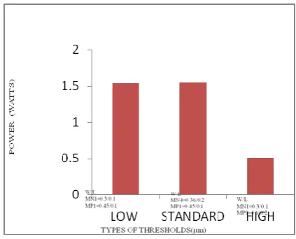
Fig 4 Describes about the power analysis in different types of threshold for 1V. It consists of Low, Standard, and High Threshold. By using the Micro-wind tool, the inverter layout for the given W/L ratios is drawn and the power is calculated from it. PMOS and NMOS W/L ratios value differ for each threshold region. The results are taken for each threshold region and comparison is done to see which threshold consumes less power. Then it is plotted by using the graph for easy comparison of the threshold regions. From the graph, we can find that the Low threshold consumes a power range of 1.5 Watts and Standard threshold consumes a power range of 1.58 Watts. High threshold is having the low power and it consumes 0.5 Watts. We can conclude that high threshold is better than the low threshold and standard threshold
Fig.1.Standard Threshold
Fig.2. High Threshold
© 2016, IRJET | Impact Factor value: 4.45 | ISO 9001:2008 Certified Journal | Page 1018 Fig 5 Describes about the power analysis in
different types of threshold for 1.2V. It consists of Low, Standard, and High Threshold. By using the Micro-wind tool, the inverter layout for the given W/L ratio is drawn and the power is calculated from it. PMOS and NMOS W/L ratios value differ for each threshold region. The results are taken for each threshold region and comparison is done to see which threshold consumes less power. Then it is plotted by using the graph for easy comparison of the threshold regions. From the graph, we can find that the Low threshold consumes a power range of 4.5 Watts and Standard threshold consumes a power range of 1.5 Watts. High threshold is having the low power and it consumes 0.8 Watts. We can conclude that High threshold is better than the low threshold and standard threshold. From the two graphs we can find that high threshold is having the low power and it is better for consuming low power consumption. High threshold is used for fast transition. It gives the transitions from low to high range. Finally, we can conclude that, Compare to the low and standard threshold, high threshold is having the better consumption and transition range.
2. IMPLEMENTAION OF CROSS COUPLED STRUCTURE
Fig 6 shows the circuit diagram of cross
coupled structure. In this two PMOS, NMOS, inverters are located. VDD is given at a rate of 1.2V. Two PMOS and NMOS are connected by using cross coupled structure. For NMOS one is cross coupled with input and other with output. Two inverters are connected between the input and output. When IN1 and VDD gets lowered the pull down transistors becomes weak and it cannot overcome the strength of the pull-up transistors and output becomes failed. To strengthen the pull-down transistors, ttransistors need to be upsized by several orders of magnitude for converting sub-threshold to sub-threshold voltages. Another method is, to use low threshold voltage for pull-down transistors and high threshold voltage for pull-up transistors in which it limits the reduction of delay. The problem is that when voltage across diode is constant, it causes
the delay scalability. To overcome this, forward bias is applied to the pull-down transistors to reduce the delay. When input is high output is low. When ‘1’ is given at input it produces the output ‘0’.
3. IMPLEMENTAION OF CURRENT MIRROR STRUCTURE
Fig7 shows the circuit diagram of current mirror structure. In this, three PMOS, inverters, and two NMOS are located. VDD is given at a rate of 1.2V. Two PMOS are cross coupled and one PMOS is connected to the inverter and output. One NMOS is connected with input and other is connected with output. In this when input is 0 output also 0. Logic error is detected when the cioutput is also 0. Logic error is detected when the output is also 0. Circuit is in the ON stage. When current mirror is controlled by sensing the logic error detection power is reduced. When PMOS in NOR gate cannot be switched off, static current is larger so we can reduce the size of PMOS and NMOS devices which slow down the output transition. Static current can be reduced by reducing the size of PMOS and NMOS transistor
[image:3.595.342.554.478.649.2]© 2016, IRJET | Impact Factor value: 4.45 | ISO 9001:2008 Certified Journal | Page 1019 Fig 5: Power Analysis in Different Types of Threshold
Inverter for 1.2V
Table1. Summary Of The Transistor Sizing For 1v
Table 2. Summary Of The Transistor Sizing For 1.2 V
[image:4.595.305.546.98.292.2]which will lead to increase in delay. It leads to fast range wide conversion. It has less contention and it provides potential for achieving small delay, low switching energy, and delay scalability.
Fig.6 Cross Coupled Structure
Fig.7 Current Mirror Structure
3.IMPLEMENTATION OF PROPOSED LEVEL
[image:4.595.306.546.323.521.2]SHIFTER
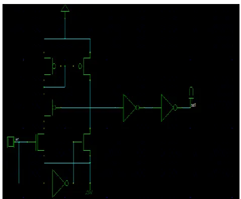
Fig 8 shows the circuit diagram of proposed level shifter. In this proposed level shifter, it is combined with current mirror technique. The implementation is done for the cross coupled structure and current mirror circuit in below figures 5.4, 5.5 to find which produces the better power consumption. Then, Current Mirror technique is used in level shifter because it yields better power consumption. In this circuit, in1 and in2 are the inputs and out1 is the output. VDD is given at a rate of 1.2V. In1 is given to the inverter and in2 is given to the level shifter circuit. Level shifter circuit is
W/L LOW STANDARD HIGH
NMOS 0.3/0.1 0.36/0.2 0.3/0.1
PMOS 0.45/0.
1
0.45/0.1 0.6/0.2
W/L LOW STANDARD HIGH
NMOS 0.3/0.1 0.36/0.2 0.3/0.1
PMOS 0.45/0.
1
[image:4.595.47.279.351.436.2]© 2016, IRJET | Impact Factor value: 4.45 | ISO 9001:2008 Certified Journal | Page 1020
combined with current mirror .technique to give the output. Level shifter is used in multi-supply because different blocks are working on different voltages so when a signal passes from one voltage domain to another voltage domain level shifter is needed particularly from low voltage domain to high voltage domain. Level shifter will shift the voltage from low voltage domain to high voltage domain or high voltage domain to low voltage domain. High voltage domain can read the logic ‘0’ or ‘1’ accurately. Usually level shifters are inserted when it is crossing from
low voltage domain to high voltage domain.
[image:5.595.55.287.308.529.2]
Fig 8.Circuit Diagram of Proposed Level Shifter
4 RESULT AND DISCUSSION
Fig 9 shows the implementation of cross coupled structure. By using the circuit diagram of Cross Coupled CMOS we got the implementation. In this input is in1 and output is out1. When input is high, output is low. The output starts from the 0 ns and it maintains constant at 1ns and it shows the little drop voltage from 0.5ns to 0.9ns. It consumes a power range of 46.434 µw.
Fig 10 shows the implementation of Current Mirror. By using the circuit diagram of Current mirror
we got the implementation. In this, input is in1 and output is out1. When input is low output also low. The output starts from 0 ns and rise at 0.1 ns and falls at 0.2 ns. The constant value maintains at 0ns. It consumes a power range of 28.351 µw.
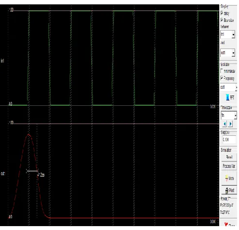
Fig 11 shows the implementation of proposed level shifter. Here the level shifter is combined with technique current mirror and it produces the output. In1 is given to the inverter and in2 is given to the level shifter circuit. Out1 starts from lower level and it got raises to the above level. This shows that the voltage shifted from the sub-threshold level to the threshold level. Sub-threshold level is the level in which it occurs below the gate region. Threshold level is the level in which it occurs above the gate region. This shows that the out1 is produced in the form of level shifting. Out3 is produced in the form of the inverter because one input is connected to the inverter. So by inserting the current mirror technique in the level shifter circuit the voltage is shifted and it consumes a power range of 31.860 µw.
[image:5.595.344.589.414.603.2]© 2016, IRJET | Impact Factor value: 4.45 | ISO 9001:2008 Certified Journal | Page 1021 Fig 10 Implementation of Current Mirror Structure
Fig 11 Implementation of Proposed Level Shifter
5. CONCLUSIONS
Thus the level shifter is used for converting the
deep sub-threshold region to the above threshold region. Low power consumption is possible, by power analysis method. By using the Micro-wind tool, the inverter layout for the low, high, standard threshold is done and the power is calculated. From the power analysis we can find that high threshold is having the
low power consumption. While shifting from one region to another region small number of delay occurs. To avoid delay, two methods are used. One method is by using, low threshold voltage for pull-down transistors and high threshold voltage for pull-up transistors in which it limits the reduction of delay and lead to larger area. Another method is, using mixed threshold device, it reduces the delay, switching energy and leakage power for wide range conversion. The circuit of cross coupled CMOS and current mirror is compared to know which is having the low power consumption. Then the current mirror technique is inserted in the level shifter to have the low power and fast transition.
REFERENCES
[1] Marco Lanuzza, and Pasquale Corsonello, “Fast and Wide Range Voltage Conversion in Multi Supply Voltage Designs” IEEE Transactions on Very Large Scale Integration (VLSI) Systems, vol.23, no.2, pp.388-391, February 2015.
[2] Jun Zhou, and Chao Wang, “An Ultra-Low Voltage Level Shifter using Revised Wilson Current Mirror for Fast and Energy Efficient Wide-Range Voltage Conversion from Sub-Threshold to I/O Voltage” IEEE Transactions on Circuits and Systems, vol.62, no.3, pp.697-706, March 2015.
[3] Ching Ji Huang, and Yuan Hua Chu, “A Wide-Range Level Shifter using Modified Wilson Current Mirror Hybrid Buffer” IEEE Transactions on Circuits and Systems, vol.61, no.6, pp.1656-1665, June 2014.
[4] S.Rasool Hosseini, and Mehdi Saberi, “A Low Power Sub-Threshold to Above Sub-Threshold Voltage Level Shifter” IEEE Transactions on Circuits and Systems, vol.61, no.10, pp.753-757, October 2014.
[image:6.595.37.284.118.355.2]