WRL
Research Report 90/1
Noise Issues in
the ECL Circuit Family
research relevant to the design and application of high performance scientific computers. We test our ideas by designing, building, and using real systems. The systems we build are research prototypes; they are not intended to become products.
There is a second research laboratory located in Palo Alto, the Systems Research Center (SRC). Other Digital research groups are located in Paris (PRL) and in Cambridge, Mas-sachusetts (CRL).
Our research is directed towards mainstream high-performance computer systems. Our prototypes are intended to foreshadow the future computing environments used by many Digital customers. The long-term goal of WRL is to aid and accelerate the development of high-performance uni- and multi-processors. The research projects within WRL will address various aspects of high-performance computing.
We believe that significant advances in computer systems do not come from any single technological advance. Technologies, both hardware and software, do not all advance at the same pace. System design is the art of composing systems which use each level of technology in an appropriate balance. A major advance in overall system performance will require reexamination of all aspects of the system.
We do work in the design, fabrication and packaging of hardware; language processing and scaling issues in system software design; and the exploration of new applications areas that are opening up with the advent of higher performance systems. Researchers at WRL cooperate closely and move freely among the various levels of system design. This allows us to explore a wide range of tradeoffs to meet system goals.
We publish the results of our work in a variety of journals, conferences, research reports, and technical notes. This document is a research report. Research reports are normally accounts of completed research and may include material from earlier technical notes. We use technical notes for rapid distribution of technical material; usually this represents research in progress.
Research reports and technical notes may be ordered from us. You may mail your order to:
Technical Report Distribution DEC Western Research Laboratory, UCO-4 100 Hamilton Avenue Palo Alto, California 94301 USA
Reports and notes may also be ordered by electronic mail. Use one of the following addresses:
Digital E-net: DECWRL::WRL-TECHREPORTS
DARPA Internet: [email protected]
CSnet: [email protected]
UUCP: decwrl!wrl-techreports
the ECL Circuit Family
Jeffrey Y. F. Tang and J. Leon Yang
January, 1990
Copyright
1990, Digital Equipment Corporation
1. Introduction
Noise in electrical systems is unavoidable. In a digital system, the main concern is that the noise has to be controlled so as not to cause a false switch resulting in system malfunction.
Noise margins are different for different circuit families. For example, the noise margin in CMOS is much better than that in NMOS circuitry because of the better transfer characteristic which results from replacing the depletion FET with a PFET. Because of the larger voltage swing, the MOS circuit families have in general much better noise margins than the ECL circuit family. Roughly speaking, the voltage swing ratio between MOS and ECL is about 10 to 1. In MOS circuit families the power consumption is mainly AC, especially in CMOS, while in the ECL circuit family DC power is the main concern. For a high power single chip ECL processor, the noise problem is further exacerbated by the high DC current demand. The immediate problem that arises is the IR drop on the power bus which in fact is the single most important noise source.
In this document, the noise margin definition, DC noise margin for ECL gates, and noise sources in the ECL environment will be discussed.
2. DC Noise Margin
In this chapter, our definition of noise immunity and unity gain noise margin will be introduced. The interpretation of noise margin in terms of the transfer curve of a basic gate is also discussed. Specifically, the transfer equation for a basic ECL gate is derived and the noise margin variation is discussed.
2.1. Definition
Noise immunity is defined as the amount of noise required at the input of the first receiving gate to cause a false switch in the subsequent gates of an infinite chain. This is depicted in Figure 2-1(a). For example, the noise immunity of a chip input receiver is the amount of cross talk, ringing, etc. that can be tolerated on the board without causing a false switch of the receiver. Since the output of a receiver is often latched, one can consider the infinite chain being replaced by the latch.
Gn+1 Gn
G1
Vn Vn
Vn
G1 Gn Gn+1
Vn
(a)
(b) G2
G2
Figure 2-1: An infinite chain of gates defining (a) noise immunity and (b) noise margin
Noise immunity is always larger than noise margin, since it only guarantees that the first receiving gate will not false switch. Noise margin more conservatively considers the cumulative effect of noise at the inputs to each gate. In practice, noise margin is a better measure. In this report we will concentrate mainly on DC noise margin. Keeping the DC noise within the noise margin guarantees functional cir-cuits.
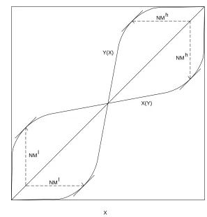
Figure 2-2 shows the transfer relation of a non-inverting gate. Both y(x), x(y), and x=y are plotted. Noise margin is defined as the distance in x (or y) from the slope-of-one point of y(x) (or x(y)) to the y=x line. Since y(x) and x(y) are symmetric with respect to the y=x line, a different way of saying this is that the edge of the largest square that can be fit into the lobes defines the noise margin. In Figure 2-3, it is demonstrated that this is in fact the same definition as depicted in Figure 2-1(b). A similar definition exists for an inverting gate by simply rotating the diagram 90 degrees.
Assume V in Figure 2-1(b) equals the noise margin (NM). As shown in Figure 2-3, starting from then
’
first input x at perfect high level and subtract NM to x0 0 which is the input level as seen by the gate, the
’
output is obtained at y through the transfer curve y(x). Since y is again degraded by NM, y1 1 1 is seen at the next input gate and x is obtained through the transfer curve x(y). Going down the paths, it eventually2
’
converges to a loop which starts at x , the slope-of-one point of x(y), to x2n 2n, the slope-of-one point of
’
y(x), to y2n+1, to y2n+1 and returns to x . If V is greater than NM, it will converge to the low side after2n n some number of gates and cause a false switch.
X(Y) Y(X)
X Y
NMl l NM
NMh
[image:7.612.169.466.112.423.2]h NM
Figure 2-2: The transfer curve of a non-inverting gate
2.2. A Basic ECL Gate
A basic ECL gate structure is shown in Figure 2-4.
Let us define the normalized input, x, output, y, and voltage swing, s, as vin−vref
x = , (1)
vT vo −Io×Rc
y = = , (2)
vT vT
and
vs −It×Rc
s = = , (3)
vT vT
X(Y)
Y(X) NM
NM Y
X
NM
l
l NM
x x
x x
x 2n
2 0
2n
x 0’
’
2
y y y
y y
2n+1 3 1
2n+1 3’
y1’ ’
’
Figure 2-3: The transfer paths of a series of non-inverting gates each having a noise source equal to NM
In the simplest approximation, I and Io ~ocan be expressed as Vbe2
I = I exp ( ),o s (4)
vT Vbe1
I~o= I exp ( ).s (5)
vT
The ratio of the two output currents becomes I~o Vbe1−Vbe2 vin−vref
= exp ( ) = exp ( ) = exp(x). (6)
Io vT vT
Since the outputs are connected to bases of either the emitter followers in the ECL configuration or the next gate in the CML configuration, the base currents are negligible. Hence,
Vcc
v ~v
R R
ref
Vee I
~o
I t
c c I
v in
v
o
o o
Q1 Q2
Figure 2-4: A basic ECL gate
From Equations (7) and (6), we get It
I = .o (8)
1 + exp(x)
From Equations (2), (3) and (8), the transfer equation is derived as −s
y = . (9)
1 + exp(x)
The slope of the curve, which is the gain of the gate, can be derived as
dy s
G = = . (10)
dx exp(−x) +2 + exp(x)
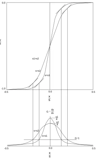
Plotting the transfer curve and the gain with both y and x normalized to s, universal transfer curves for the basic ECL gate are obtained for two different normalized voltage swings, s1 and s2, as shown in Figure 2-5.
Note that both the transfer curve and its derivative, the gain, depend only on s, the voltage swing which is normalized to the thermal voltage v . The larger the voltage swing, the narrower the transition region, theT higher the voltage gain at threshold (x=0) and, obviously, the larger the noise margin.
To derive the noise margin as a function of the voltage swing, we replot the transfer curve of a non-inverting gate in Figure 2-6 with the geometrical representations of noise margins. Setting G, the gain, to one we get
h l
xg = ln(s−2) and x =g −ln(s−2) (11)
0.0
s y
-1.0
0.5 0.0
x
-0.5
s
-0.5
s x
0.0 0.5
dy dx G
G 1 s=s1
s=s2
s=s2 s=s1
[image:10.612.128.436.98.604.2]s2 4 s1 4 s1>s2
t g t
x = y + 0.5 s
y
0.0 0.0
l g x xl
x
0.5s -0.5s
-s
xh h
xg
t t
x -x =
NMl l l NM = x - gh th xh
a s
2
a a
[image:11.612.161.467.89.432.2]b
Figure 2-6: The transfer curve of a non-inverting gate with the geometrical representations of noise margins
h l
−xg xg
2>>e and 2>>e . (12)
The superscripts indicate whether the logic level is either high or low.
Combining Equations (11) and (12), this assumption can be reduced to
s >> 2.5. (13)
For all practical purposes, this is always true. For example, for 125°C and a voltage swing of 500 mV, s ~ 14.58, one sees that Equation (13) is well satisfied. Since the transfer curve is symmetric, we shall derive the high noise margin only. From Figure 2-6, the high noise margin is simply
s
h
NM = −a−b, (14)
2
s
h h
where a =|y(x )t |= from Equation (9), and b = x = ln(st −2). Thus,
s−1
s s
h h h
NM = xt −xg = − −ln(s−2). (15)
l
Similar derivation for the low noise margin, NM , yields the same formula.
2.3. Noise Margin Variation
As pointed out in the previous section, noise margin for an ECL gate is only a function of the normalized voltage swing. Noise margin will only vary through variations of the normalized voltage swing.
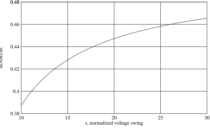
The derivative of high noise margin with respect to s is
h
dNM 1 1 1
= + − . (16)
2
ds 2 (s−1) s−2
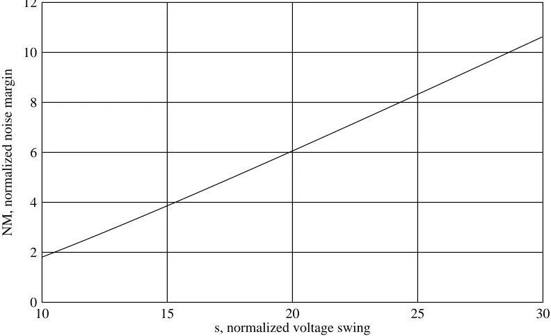
Equations (15) and (16) are plotted in Figures 2-7 and 2-8 respectively. Once the voltage swing of an ECL differential pair is known, the noise margin and its derivative with respect to the swing can be easily determined from the plots.
10 15 20 25 30
s, normalized voltage swing 0
12
2 4 6 8 10
[image:12.612.59.455.293.535.2]NM, normalized noise margin
Figure 2-7: Normalized noise margin versus normalized voltage swing
10 15 20 25 30 s, normalized voltage swing
0.38 0.48
0.4 0.42 0.44 0.46 0.48
d(NM)/ds
Figure 2-8: Derivative of normalized noise margin versus normalized voltage swing
274 282 308 310 317 850 750
271 263 247 236 229
23.53 T v [mV]
25.85 30.58 34.30 36.58 0
27
125 155 85
400 500 600
201 111 156
105 93 85
149 135 126 79 120
194 179
162 169 Voltage Swing [mV]
Temperature [C]
[image:13.612.99.506.84.332.2]Noise Margin [mV]
3. DC Noise Sources
The nature of noise and various noise source types in an ECL environment will be discussed. Here, two types of noises are distinguished, intrinsic and extrinsic. Intrinsic noise is the type of noise associated with specific circuit configurations such as multiple fan-in, series gating, etc. Extrinsic noise is the type of noise associated with the circuit environment, such as ohmic drops on metal lines, temperature dif-ferences, short and long range process variations, etc.
3.1. Definition
As depicted in Figure 3-1, anything that causes v -voh refor vref-volto degrade is defined as a noise source.
h
The degradation of the former causes high noise margin NM to degrade while the degradation of the
l
latter causes low noise margin NM to degrade. For example, if a certain IR drop causes all v , v , andoh ol vrefto shift up by∆, there is no degradation of the noise margin. But if it only causes vrefto shift up by∆,
h l
NM decreases while NM increases by∆.
v ref
v ol oh v
ref
v 0.5Vs
0.5Vs v
[image:14.612.102.454.311.415.2]oh ol v
Figure 3-1: Definition of noise for a differential pair.
3.2. Intrinsic Noise
Intrinsic noise occurs in certain types of circuit configurations. In this section we will discuss three basic types of noise arising from current sharing, incomplete switching and Vbevariations of level shifting.
3.2.1. Current Sharing Noise
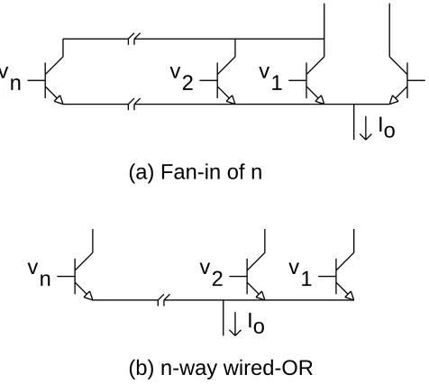
Noise arising from current sharing is ubiquitous in ECL designs. Typical examples are gates with mul-tiple fan-in, wired-OR (emitter-ORing) and emitter-ANDing (in multi-emitter decoders, diode decoders, or EFL circuits), as depicted in Figure 3-2.
The fundamental problem here is that any of the n-way input transistors can possibly take all I or 1/n I .o o From the basic Equation (4), the difference in Vbeas a result can be expressed as
∆Vbe= v ln(n).T (17)
o I
Io
(c) 6-way emitter-ANDing (b) n-way wired-OR
v
2 v1
v n
o I
(a) Fan-in of n n
v
1 v 2
[image:15.612.98.336.61.274.2]v
Figure 3-2: Typical examples of circuits with current sharing noise
3.2.1.1. Multiple Fan-In
n-transistors m-transistors
ref v
R R
o ~o
Vee I
~o
Vcc
I t
c c Io
v
in v2 v1
Figure 3-3: A generalized ECL gate
Figure 3-3 depicts an ECL gate with fan-in of n on the input side and m transistors in parallel on the reference side. These transistors are of the same size. Analogous to the derivation of Equations (6) and (9), if we assume that all n inputs are switching together, we have
I~o n
= exp(x), (18)
Io m
[image:15.612.95.549.355.557.2]−s −s
y = = . (19)
n n
1 + exp(x) 1 + exp[x + ln( )]
m m
n
Assuming n > m, the transfer curve is shifted by ln( ) toward the negative x direction. This is shown in
m
[image:16.612.99.264.71.110.2]l l
Figure 3-4 as y . In unnormalized terms, this means that the low noise margin NM has decreased and the
n
h
high noise margin NM has increased by an amount v ln( ). For m equal to one, this is exactly the sameT
m
as Equation (17). This is the worst case for the low noise margin but not for the high noise margin. Similar to Equations (11) and (15), the unity-gain point and the low noise margin are obtained as
n
l
x =g −ln(s−2)−ln( ) (20)
m
and
s s n
l
NM = − −ln(s−2)−ln( ). (21)
2 s−1 m
ln(n/m)
h y y
0 l y
xgl xgh
y
0.0 0.0
x
0.5s -0.5s
-s
ln(m)
[image:16.612.68.448.200.655.2]If one and only one of the n input transistors is switched against the m parallel reference transistors while all other n-1 inputs stay at the highest possible low x but within the noise margin, Equation (19) becomesL
−s −s
y = ≈ , (22)
1 n−1 1 + exp[x−ln(m)]
1 + exp(x)+ exp(−|xL|)
m m
assuming
n−1 n−1 l n−1 1
exp(−|xL|) < exp(x ) = g << 1 , (23)
m m n s−2
which is a similar condition as dictated by Equation (13).
l
Note that x < xL g is required to satisfy the low noise margin. In this particular case, the transfer curve is shifted by ln(m) towards the positive x direction. Therefore, the high noise margin has decreased and the low noise margin has increased by v ln(m) as shown in Figure 3-4. Similarly, the unity-gain point andT the high noise margin are obtained as
h
xg = ln(s−2) + ln(m) (24)
and
s s
h
NM = − −ln(s−2)−ln(m). (25)
2 s−1
From Equations (21) and (25), one sees that if m is set to√n, the high noise margin is the same as the low noise margin, and the loss of noise margin as compared to the basic gate becomes v ln(T √n) = 0.5 v ln(n).T This is only one half of that described in Equation (17).
If the inverting output is considered, as shown in Figure 3-5, the result is just the opposite. Where noninverting outputs suffer losses of high noise margin, inverting outputs suffer losses of low noise margin by the exact same amount.
Here are the guidelines:
•The effect of having n input transistors (or one input transistor with n times the size) switched against one reference transistor is to shift the reference voltage down by v ln(n). For aT noninverting output, it means the low signal level suffers a degradation of v ln(n), but theT high signal level suffers no degradation. However, for an inverting output it means the high signal level suffers a degradation of vT ln(n), but the low signal level suffers no degradation. •For a gate with a fan-in of n, the loss of noise margin can be reduced to 0.5 v ln(n) if theT
reference transistor is sized up by√n as compared to the input transistors. When the tran-sistor is resized, losses of noise margin for high and low signal levels are equal for both inverting and noninverting gates. However, increasing transistor size will naturally increase capacitances. Tradeoffs between DC noise margin and AC perfomance must be considered.
3.2.1.2. Wired-OR Configurations
-s
-0.5s 0.5s
x
0.0
0.0
y
h y y
0 yl
ln(m)
[image:18.612.128.432.112.428.2]ln(n/m)
Figure 3-5: The inverting transfer curve of a generalized gate
shifted up by v ln(n). As depicted in the figure, if vT refis shifted up by 0.5v ln(n), the resulting level willT be exactly in the middle of the worst case output levels, which is in the center of the lowest high (one transistor on) and the highest low (n transistors on).
v o
Q1 Q2 v
ref
Io vn
oh v
1-on
ol v n-on
n-on ref v
(a) v
v2 1
ln(n) T v 0.5
(b) v ln(n)
ln(n) T v
T
[image:18.612.58.519.524.673.2]There are two ways of achieving this goal. One can either literally shift the reference voltage up by 0.5v ln(n) with customed circuitry, or, as described in the first guideline above, one can size up theT reference side transistor, Q , by2 √n. Here are similar guidelines:
•For an n-way wired-OR driving a differential pair, the loss of noise margin is only 0.5 v ln(n) if the reference transistor Q is sized up byT 2 √n as compared to the input transistors Q of the differential pair. If the reference transistor remains the same size as the input1 transistors, for noninverting gates there is no loss of noise margin for high inputs, but the loss of noise margin for the low inputs will be v ln(n).T
•If the n-way wired-OR is not driving a complex gate with multiple fan-in where simple resiz-ing cannot be done without affectresiz-ing other inputs, the loss of noise margin takes the full value of v ln(n). In this case, the important parameter is the sum of n for wired-OR and number ofT OR inputs at the lower level.
3.2.1.3. Emitter-ANDing
For emitter-ANDing, similar optimization to wired-ORing can be applied if it is driving a differential pair. For example, as depicted in Figure 3-2(c), the output of the 6-way decoder has its output low level shifted up by v ln(6). Assuming the output is to be compared to a reference voltage, one can shift up theT reference by 1/2v ln(6) to halve the noise.T
Other situations may arise from application to application. Based on what has been discussed, one can easily figure out the loss of noise margin due to current sharing type circuits.
3.2.2. Incomplete Switching Noise
Incomplete switching is defined as shown in Figure 3-7. The problem here is that the degraded upper tree ′
current results in a loss of low noise margin. If we defineρ= I / I , then the loss of low noise margin ist t simply
l
∆NM = v (1s − ρ) , (26)
where v is the swing corresponding to I .s t
Multi-level series gating is the obvious candidate. Both two-level and three-level series gatings will be
’
discussed. The degradation of I will also be considered, as well as the method of compensating thist incomplete switching noise.
3.2.2.1. Two-Level Series Gating
Figure 3-8 shows one case of a multi-level series gated ECL gate where the lower level consists of a simple differential pair. Here, the concern is that when the current is steered through transistor Q in thea
’ ’
worst case, what is the relation between I and I ? Ideally, if I = I there is no loss of noise margin due tot t t t the extra level of series gating because the voltage swing for the upper level remains the same. Consider
’
the single-ended case where v =vb ref. Referring back to Figure 2-6, the worst case I occurs when v -vt a ref
h
is at x . In this situation the inputs have lost all the noise margin and are at the unity-gain point.g From Equations (6) and (11), we get
′ It
h
= exp(x ) = sg −2, (27)
upper tree lower tree ’ t I t I I t <
Figure 3-7: The definition of incomplete switching
v a t I ref v n
1- way
Qb a Q b v ’ t I a ii ) ~v
ref i ) v =
) ( It - It’ vs
s
[image:20.612.161.473.258.417.2]v (1 - I ’ I t )t
Figure 3-8: Two-level series gating
or
′ It s−2
= . (28)
It s−1
As depicted in Figure 3-8, where the thick lines represent the unperturbed signal levels, the amount of loss in the low noise margin can be expressed as
′ It vs
l
∆NM = v (1s − ) = . (29)
It s−1
Note that the high noise margin is in fact slightly improved since vohcan only become more positive due to the incomplete switching.
In the case where v =~v , where the gate is being differentially driven, the worst case occurs when v is atb a a
h l
xg and v is at x . Similar to the above derivation, we haveb g
′ 2
It (s−2)
= (30)
2
and
vs
l
∆NM = . (31)
2
(s−2) + 1
Note here that the differential signal swing only needs to be half the voltage swing since all common-mode noise is excluded. In fact, the noise margin of a half swing differential drive is much better than a full swing single-ended drive. Figure 3-9 depicts another case of two-level series gating where the lower level has a fan-in n . Assuming that the reference transistor is properly sized up by2 √n according to the2
′
guideline discussed in section 3.2.1, the worst case I occurs when all of the n inputs are at the unity-gaint 2 point corresponding to the multiple fan-in case as described by Equation (20). With n/m=√n , the current2 ratio becomes
′
It 1
l
= exp(−x ) = sg −2, (32)
′ It−It √n
2
which is the same as Equation (27). Accordingly, the loss of noise margin is the same as that in Figure 3-8 which is described by Equation (29). The degradation of the tree current due to the case of a second level multiple fan-in is the same as that of a simple second level pair driven differentially. This is naturally true considering the way the down-shift of the unity-gain point was derived. All we really need to differentiate is whether the second level is driven differentially or single-endedly.
2 n - way I
t ’
I t 1- way
[image:21.612.185.544.364.529.2]n vref ) t I ’ (1 - I t vs s v ) ’ - I t t I (
Figure 3-9: Two-level series gating with multiple fan-in on the lower level
3.2.2.2. Three-Level Series Gating
A three level series gated structure is shown in Figure 3-10. Based on the previous discussion, there are ′′
three possible relations between I and I , depending on whether the lower levels are driven differentiallyt t or single-endedly.
Case 1: if all lower levels are driven single-endedly, from Equation (28), we get ′′
It s−2
2
= ( ) . (33)
1 2 3 ref ref ’ ’ vref t
’- It ’’ )
’ b ’ ’ ’ ’
ii ) ~v
ii ) ~v a Q v a ’ ’ ’ I )
I t
= i ) v a v b b Q Qb v a i ) v =
t I n
1- way
t I ( I t vs s v (1 - It
a v
Qa
R c
[image:22.612.158.519.87.366.2]R cs
Figure 3-10: Three-level series gating
Case 2: if one of the lower levels is driven differentially and one single-endedly, from Equations (28) and (30) we get
′′ 2
It s−2 (s−2)
= . (34)
2
It s−1 (s−2) + 1
Case 3: if all lower levels are driven differentially, from Equation (30) we get
′′ 2
It (s−2)
2
= ( ) . (35)
2
It (s−2) + 1
3.2.2.3.αDegradation
In Figure 3-11, a path of a three level tree is shown. Assuming the current switches one hundred percent to the path shown, there is still the degradation of current due to the base current as we move up the tree.
n
The percentage degradation in the voltage swing can be expressed asρ= (1− α), where n is the number of levels of series gating. Ifα= 0.99, each extra level causes a loss of low noise margin of one percent of the voltage swing. Note that the effect is the same as that of the multi-level series gatings.
I t I
t I
t
2
= =
= 3
t I ’
’ t I
’’ t I
2nd level 1st level
3rd level I
t ’
R cs R
[image:23.612.185.357.89.423.2]’ c
Figure 3-11: αdegradation
n
An alternative is to modify the ratio of R and Rc cs such that R =c α Rcs so the degraded tree current generates the desired swing. There are three problems to this solution. Unless the layout grid is fine enough, one might not be able to resolve the 3% difference in resistances in the case ofαcompensation. In addition, the matching is degraded. Secondly, in the case of multi-level series gatings, since one does not always get the worst case condition, the added swing slows down the switching speed. Most seriously, βusually is not well controlled. It is difficult to predict the value forα.
Here are the guidelines:
l
•All cases of multi-level series gating result in a loss of low noise margin, as∆NM =v (1s − ρ), where ρis the ratio between current actually flowing through the resistor load and the total tree current.
•If the incomplete switching gate drives a simple differential pair similar to that discussed in a wired-OR situation, the reference voltage of the driven gate can be shifted to halve the noise. •The ratio of R to Rc cs can be modified to compensate the current degradation. Care should
3.2.3. V Variations of Emitter Followers
beThe emitter follower plays a very important role in ECL designs. It drives the capacitive load and shifts the signal level down to the desired value. One of the most important matchings in ECL designs is, in fact, the matching of the current density of the emitter follower, which guarantees matching of the diode drops in various parts of the circuits.
3.2.3.1. Pull-Down Resistors
In some ECL designs, a -2 volt power supply commonly referred to as Vee2is used to generate the current source for emitter followers. As depicted in Figure 3-12, one sees that the current of the emitter follower changes as the output switches states. This results in variations of the diode drop Vbeand hence a loss of noise margin as depicted in part (b) of the figure. Again, thick lines in the figure show the unperturbed levels. Assume that the emitter follower and the pull-down resistor are sized with respect to some mean current I . In order to balance both the high and the low side, it is required thato
Ioh Io
∆h = v ln( )T ≡ ∆l = v ln( ) T . (36)
Io Iol
vref ref v (c) (b) I o ol I oh I I o h il v be_l v vbe_h vih l (a) I o sized according to I
be v R il v ih v ol v oh v ee2
V = Ioh I ol
[image:24.612.61.522.249.536.2]R
Figure 3-12: Pull-down resistors for emitter followers
As depicted in part (c) of the figure, I is simply the geometric mean of Io ohand I .ol The value of the resistor is determined by
√(voh−vee2) (vol−vee2)
R = , (37)
Io
and the loss of noise margin can be easily derived as
voh−vee2
∆= v ln(T √ ) . (38)
For example, if v =-0.9, v =-1.4, Voh ol ee2=-2.0, and v =0.03, thenT ∆=9.1 mV. Strictly speaking, the for-mula needs to be iterated to take into account the fact that the vohand volvalues are changed as Vbeis modified. But the computation error is very small and is hence neglected here. Note that the IR drops on the power distribution and the power supply variations are not accounted for here. In later sections where IR drops are discussed, the noise discussed here will be revisited.
3.2.3.2. Fan-Out
The fan-out issue is usually not a concern unless the fan-out is large or the tree current of the driven gate is large. Figure 3-13 shows two situations of fan-out. Part (a) consists of a pull down resistor while part (b) consists of a real current source.
ih v v I be il v ol v oh v ee2 V R n
fanout* Ib
R
o
sized according to I = I oh Iol
v vih
[image:25.612.126.553.233.416.2]* I b fanout n V voh vol vil be I o (a) (b) ee1
Figure 3-13: Multiple fan-out
The basic problems are exactly the same as that discussed in the previous section. For part (a), the equations for high and low output current are expressed as
voh−Vee2
I = + noh fan−out×I ,b (39)
R and
vol−Vee2
I = .ol (40)
R
For part (b), the equations for high and low output currents are I = I + noh o fan−out×I and I = I , respec-b ol o tively. Given a desired current I , one can easily figure out the loss of noise margin by the followingo equations
Io
h
∆NM = v ln( )T Ioh and
Iol
l
In practice, the emitter follower will not be resized unless the fan-out current loading is extremely large. Since the fan-out current loading is only active when output is in the high state, the extra loss of the high noise margin can be simply expressed as
Ioh Infan−out×Ib
h
∆NM = v ln( ) =T −v ln(1+ ).T I + noh fan−out×Ib Ioh
For example, if the fan-out current loading is 10% that of I , the extra loss of noise margin on top of theoh emitter follower is only about 2.86 mV at 85°C. So if 3 mV is allocated in the noise budget for fan-out, it is equivalent to say that nfan-outx I has to be less than 10% of I .b o
3.3. Extrinsic Noise
Extrinsic noise is the result of the realistic environment where the circuit operates. The variations of the environment parameters cause the signal levels to drift, resulting in loss of noise margin. The noises caused by the IR drops in interconnect lines and the different types of variations that cause changes in device parameters or drifts of signal levels will be discussed.
3.3.1. IR Drops
The issue of IR drops on the power distribution is particularly a problem in ECL designs for two reasons: small DC noise margin and large DC current. In this section, the noise implications of different types of IR drops will be discussed.
3.3.1.1. IR Drops on the Top Rail
When an IR drop∆occurs on the top rail (the Vccsupply line) between the sending gate and the receiving gate reference generator,∆amount of either high or low noise margin is lost, depending on the polarity of the drops. Figure 3-14 depicts the situation corresponding to a loss of low noise margin and a gain of high noise margin.
v oh
ol v
[image:26.612.59.393.502.676.2]ref v
It can be seen from the figure that if the polarity of ∆ is reversed, a gain of low noise margin at the expense of high noise margin results. In theory, this type of noise can be halved, provided that the differential pair is properly sized. In practice, this is hard to do since ∆ might not be a well managed quantity. If multiple fan-in exists, there is no way to optimize the gate because inputs are coming from different parts of the chip.
Here is the guideline:
•IR drops on the top rail always translate into a change of (v -voh ref) or (vref-v ), causingol direct loss of either the high or low noise margin.
3.3.1.2. IR Drops on the Bottom Rail
The bottom rail, Vee1, is the reference rail for all current sources. A band gap generator generates a regulator voltage which is one diode drop plus a voltage swing (v +v ) above the bottom rail. The mainbe s effect of IR drops on Vee1bus is to cause a change in current generated by current sources.
V Generator Upper tree
C.S. for EF
ref
vR R
v vR
= R v V
Reg
v s
v v
s be
V cc
[image:27.612.95.530.272.504.2]V ee1
Figure 3-15: IR drops on the bottom rail, Vee
Figure 3-15 depicts three different situations: a current source for a tree, a current source for an emitter follower and a current source for a reference generator. Also shown in the figure is that the voltage across the current source resistors becomes v -s∆due to the IR drop.
In the case of a tree, the voltage swing is degraded by∆. Using the notation before, this is equivalent to ρ= 1-∆/ v . A loss of low noise margin ofs ∆results. The discussion in the previous section applies.
In the case of a current source for an emitter follower, the change in current due to the IR drop induces a change in the Vbeof the emitter follower, resulting in signal degradation. The loss of noise margin is
∆NM = v ln(1T − ∆/v ).s
The noise associated with reference generators will be discussed in Section 3.4.
The IR drop on the other bottom rail, Vee2, directly affects the emitter followers with a pull-down resistor as discussed in section 3.2.3.1. In most digital circuits, this is the only place Vee2is used. From Equation (38) we see that ∆is subject to both vohand volvariations which result from V , Vcc ee1, and Vee2 varia-tions. In the worst case, the equation can be re-written as
(voh− ∆v )oh −(vee2+∆vee2)
∆= v ln(T √ ), (41)
(vol− ∆v )ol −(vee2+∆vee2)
where ∆voh and ∆vol are functions of ∆Vcc and ∆Vee1. As discussed earlier, ∆v =oh ∆Vcc and ∆v =ol ∆V +cc ∆Vee1, since they are translated directly into variations of the signal levels. Let us plug in some numbers here. Assuming v =-850 mV,oh ∆v =150 mV, v =-1350 mV,oh ol ∆v =175 mV, vol ee2=-2.0 V, ∆vee2=100 + 150 = 250 mV (i.e. 5% of vee2and IR drop on the Vee2line), and v =30 mV (T=85T °C), the loss of noise margin,∆is 0.5 v ln(3.33) = 18 mV.T
In chapter 4, the concept of virtual Vccand statistical distribution of the∆Vcc and∆V ’s will be intro-ee duced. Equation (41) will be revisited and modified.
3.3.1.3. IR Drops on Signal Nets
Two cases of IR drops occurring on signal nets are depicted in Figure 3-16. In general, the IR drop induced by the base current is less of a concern than the IR drop induced by emitter current. But when the signal net is long or the fan-out is large, the product of I and R is no longer negligible, and the degrada-tion of signal levels has to be considered. In practice, the case one must pay attendegrada-tion to is the long wired-OR lines. The left half of Figure 3-16 shows that ∆ , the IR drop, causes a down shift of both signal levels. Assuming that the reference voltage stays at the unperturbed level, a loss of high noise margin of∆results.
r r
I a
v a
a b
b a
v o
v b I
b
[image:28.612.125.488.462.619.2]I o
Figure 3-16: IR drops on signal nets
The current ratio for the differential pair is derived as Ia va−vb I ra a−I rb b
= exp( ) exp(− ) = exp( x− δ), (42)
Ib vT vT
I ra a−I rb b va−vb
whereδ= , and x = .
vT vT
Similar to the case of a basic ECL gate, the transfer curve in this case is derived as −s
y = , (43)
1 + exp(x− δ)
where s and y are the normalized voltage swing and output. This equation is not straightforward to solve since I and I are functions of x. Let us make the following observations. At the threshold where I = I ,a b a b the mid-point of the transfer curve is shifted by an amount
δ= 0.5 I (ro a−r ) ,b (44)
whereδ> 0 if r > r , anda b δ< 0 if r < r .a b
If we assume that the dependence ofδ on x is weak near the unity-gain point, similar to the derivation
h l h l
before, we have x = ln( sg −2 ) +δhand x =g −ln( s−2 ) +δl, whereδh=δ(x ) andg δl=δ(x ).g
h
At x , we haveg
s−2 1
I =a I , I =o b Io s−1 s−1 and
s−2 1
δh Tv = ( ra− r ) I .b o (45)
s−1 s−1
l
Similarly at x , we haveg
1 s−2
I =a I , I =o b Io s−1 s−1 and
1 s−2
δl Tv = ( ra− r ) I .b o (46)
s−1 s−1
If δh > 0, a loss of high noise margin occurs. On the other hand, if δl < 0, a loss of low noise margin occurs.
s−2
For example, if r =0 there is a loss of high noise margin ofb r Ia o≈r I , while the low noise margin hasa o
s−1
1 s−3
gained by r I . If r =r =r there is a loss of high noise margin ofa o b a r Ia o≈r I and a loss of low noisea o
s−1 s−1
margin of r I . This slight asymmetry is a result of the approximation.a o
Here are the guidelines:
•If a finite resistance exists between the emitters of a differential pair and the common node that connects to the lower tree, the threshold voltage and the noise margins are modified according to Equations (44) (45) and (46).
•For the non-inverting output, the resistance between the emitter of the input transistors and the common node tends to decrease the high noise margin, while the resistance on the other side tends to decrease the low noise margin.
•For the inverting output, the result is the reverse. The resistance between the emitter of the input transistors and the common node tends to decrease the low noise margin, while the resistance on the other side tends to decrease the high noise margin.
3.3.2. Variations of Device Parameters and Operating Environment
Three different types of variations will be addressed: process variations, temperature variations and power supply variations. In short, the first two types of variations give rise to device parameter variations while the last type affects circuits that depend on V -Vcc ee1 and/or V -Vcc ee2. The main concern for a circuit designer is to understand how his or her circuits will be affected by the variations and how some of the variations can be minimized by circuit design and layout matching techniques.
In ECL designs, basic matchings are expected of (a) transistor characteristics of both input and reference devices, (b) top and bottom resistors in a tree, and (c) V ’s of emitter followers. Since the short rangebe process variation is small, good trackings of input transistors and reference transistors can always be expected, as these transistors are usually physically adjacent. Only when a tree structure is physically apart do we need to consider variations in the transistor characteristics. By the same token, the top and bottom resistors in a tree are also well matched if they are laid out the same way. Except for the α degradation discussed earlier, the voltage swing is translated from the bottom resistor to the top resistor one for one even though the current may vary. In most cases, matching considerations for both (a) and (b) are not much of a problem.
The matching of (c) ensures the correct levels for both signals and references. Intrinsic noises related to (c) were discussed in section 3.2.3. In the extrinsic case, there is the change of Vbedue to direct varia-tions of either temperature or processing nonuniformity. There is also the indirect change of Vbedue to resistance variations of the current source resistor. Let us derive the equations. Assuming the voltage across the current source resistor, V , is fixed, the current is simply I = V / R , where R is the meanR o R o o value for the resistance. The change of current due to the change of resistances follows
∆Io ∆Ro
=− . (47)
Io Ro
The change of Vbecan be derived as
1± ∆Io ∆Ro
∆V = v lnbe T = v ln ( 1T ± ) . (48)
Io Ro
3.3.2.1. Process Variations
Process variation is a strong function of the technology. In descending order of degrees of variations, there are lot to lot variations, wafer to wafer variations within a lot, and long range and short range variation within a die. Usually, one only worries about the lot to lot variation which gives the worst case tolerances, and the short and long range variation which concerns tracking of devices in close vicinity and on opposite corners of the chip.
Types
ppoly
(within a slice) Resistor
be
V +3 mV -1.2 mV / C
( 5-wide ) Implant
( 3-wide )
Implant +5%
+12% + 8% + 5%
+20%
+2% +2% +2% ( 8-wide )
( 8-wide ) +20% +5% Tolerances
Process variation
(lot to lot) Process variation
Temperature Coefficient
Temperature variation ppoly
% / C
800
800 600
0.1 Implant
600
Implant 4K 4K
0.29
Metal
0.4 - 0.1
[image:31.612.200.518.182.561.2]TC
Table 3-1: Device parameter tolerances due to process and temperature variations
All device parameters are subject to process variations. Table 3-1 shows an example of typical depen-dencies of selected device parameters on process and temperature variations. Note that the table is by no means complete and these numbers will vary depending on the technology.
the particular types. Taking the 8-µm wide 800 Ω poly resistor and the 8-µm wide 600 Ω implant resistors, for example, the worst case loss of noise margin is about 7 mV at 85°C.
3.3.2.2. Temperature Variations
Depending on the operation environment, temperature variations occur resulting in variations of device parameters. There are two types of variations: local variations (temperature gradients due to hot spots), and global variations (changes of operating temperature).
On-chip temperature gradients occur when hot spots consuming significantly larger than average power exist. Since the Vbediode drop has a negative temperature coefficient in the range of -1.2 to -1.5 mV/C, the Vbedifference is 24 to 30 mV for two junctions with a temperature gradient of 20°C. Depending on which junction has a higher temperature, the driving gate or the receiving gate reference generator, it can either cause a loss of low or high noise margin of ∆ V , since it translates directly into a shift of thebe signal level and/or the reference level.
Since no chip package is ideal, some finite thermal resistance always exists. The seriousness of this type of noise is largely a function of the packaging technology and the power consumption of the chip. Given a package technology and an estimated worst case temperature gradient, the potential loss of noise margin is figured into the noise budget.
Temperature variation as a whole is a slightly different issue. For example, the chip has to be guaranteed to work over a junction temperature from 27 to 125°C in typical commercial specification, and from 0 to 155°C for military specification. For noise margin the concerns are twofold: the variation of the output of the band gap generator which relates to the voltage swing, and the variation of the thermal voltage related noises. The guideline here is to figure out the worst case junction temperature and its associated worst case noise.
There are other device parameters that change with process and/or temperature variations. For example, the transistor current gainβcan vary 20% from lot to lot and it increases with increasing temperature. If a particular circuit design is based on some averageβ, the loss of noise margin resulting from the drift of the operating point due to the variation ofβshould be considered in the noise budget. For example, when a PNP current mirror is used, one has to estimate the average β to compensate for the base current in order to mirror the desired amount of current. In such a situation, the percentage variation of the mirrored current resulting from theβvariation should be included as a noise source.
3.3.2.3. Power Supply Variations
Power supply variation depends on a lot of factors. It is usually included in the chip specification. Circuit designers assume, for example, that no more than plus or minus five percent variation occurs on the power supply. It is the job of the package and board designers to guarantee the specification. Note that the power supply variations of concern here are global in the sense that all circuits on-chip see the same effect while the variations caused by local IR drops were considered in the previous section.
3.4. Noise from Reference Voltage Generation and Distribution
Usually on a chip, there are two units which are related to generation of reference voltages: the generation and distribution of Vcsor Vreg, the regulated voltage which is one diode drop above V ; and the genera-cs tion of V ’s from Vr reg or V . The circuits used to generate Vcs cs or Vreg usually are referred to as the master reference generators, and the circuits used to generate V ’s usually are referred to as the slaver reference generators.
3.4.1. Noise Associated with Master Reference Generators
Noise associated with master reference generators is essentially noise associated with IR drop on the bottom rail, as shown in Figure 3-15. Of course, base current also generates IR drop, but it is much smaller than IR drop on the bottom rail. In practice, a master reference generator services a number of slave reference generators which are arranged physically in such a fashion that the total IR drops are limited. It is a trade-off between the design constraints and the noise budget. An example will be given in Chapter 4.
3.4.2. Noise Associated with Slave Reference Generators
On the other hand, noise associated with slave reference generators is essentially generated by base cur-rent. V ’s are our notation for reference voltages applied to the bases of the differential pairs. Vr r0is the reference for the CML level. V , V , and Vr1 r2 r3are the ECL levels with one, two and three diode drops from the CML level, respectively.
In Figure 3-17, (a) shows the generation of V , (b) shows a basic CML gate where the signal levels arer0 generated, and (c) shows the relation between the output high and low and the reference voltage Vr0 where the thick lines represent the ideal, unperturbed levels. Superscript r indicates those notations are with respect to reference.
Vol h
R Ics
R 2
(a)
I Io
Ics
R
Voh
r r
o r
r
r r0
r0 V V
r0 V
[image:33.612.138.500.475.660.2](c) (b)
Notice that I varies from Io o maxto Io minas output varies from Vohto V , and Iol o minwill be zero if the output is not shifted down to lower levels. The signal levels, Vohand V and the reference level, Vol r0can be expressed as
r
r V I
R r r s o
V =r0 − (Ics + I ) =o − (1 + ),
r
2 2 Ics
Iomax V =oh −R Iomax=−Vs
Ics and,
Iomin
V =ol −R (I + Ics omin) =−V (1 + ),s (49)
Ics
r r
where R Ics = R I = V , the logic swing, is assumed. The loss of noise margin follows ascs s
r
Iomax Io
h
∆NM = Voh−Vr0−V /2 =s −V (s − ),
r
Ics 2Ics and
r
Io Iomin
l
∆NM = Vr0−Vol−V /2 =s −V (s − ). (50)
r I
2Ics cs
Note that a loss of noise margin occurs when ∆NM < 0. The complication here is that the difference
r
between Iomaxand Io depends on the state of the gates. From the above equations, we see that the worst
Iomax Io_FO Iomin
r
h
case loss of high noise margin is ∆NM =−V ( ) =s −V ( s + ) for I =0. Let us define fan-outo
Ics Ics Ics
(FO) as the current loading in the unit of I /csβ. The loss of the high noise margin becomes V (FO+1)/s β. The "1" in the numerator is to account for the base current of the level shifter, if there is one. If the CML gate is driving an identical gate ( I ’s are the same), then FO will correspond to the actual number ofcs driven gates. For β=100 and FO=4, 5% of the voltage swing is lost to noise in the worst case. This corresponds to 30 mV for a 600 mV voltage swing.
r
Io max Iomin
r r
l
The worst case loss of the low noise margin is∆NM =−V (s − ) for I = Io o max. By comparison,
r I
2Ics cs r
Io max Iomax 2 Iomin
h l
we see that if = + , ∆NM ≈ ∆NM in the worst case, and the fan-out for the reference
r I I
2Ics cs cs
r
voltage Vr0is twice that of the circuit fan-out, assuming Ics = I and Ics ominis negligible. Here are the guidelines:
•The loss of high noise margin due to the generation of Vr0 and CML signal levels is V (FO+1)/s β. The loss of low noise margin is the same if the fan-out for the Vr0 generator,
r r
FO =2*FO*Ics/I .cs
r
•If one desires a higher fan-out for the Vr0generator, one simply sizes up Ics to allow larger
r r r
[image:34.612.53.520.109.335.2]I . FO will be scaled by the ratio of Io cs and I , by definition.cs
Figure 3-18 shows the generation of Vr1and V . The only difference between Figure 3-18(a) and (b) isr2
r
levels. Here we will derive the noise associated with V , the result of which can be easily generalized tor1 Vr2and V .r3
Q ef r ef Q r r R 2 Ief I I Ics 2 R Ief cs I R Io Io3 ef I cs r1 V h l ef Q oh V Vol r r r r r r r o2 I V V Ior
V V R R Rr ef r r Rr Rr o2 I Io3 o r
I = Io2 + Io3
[image:35.612.98.555.87.544.2](a) (b) (c) (d) r1 r2 r1 r2
Figure 3-18: Vr1and Vr2and generation
Similar to the Vr0discussion, the signal levels V , V , and Voh ol r1can be expressed as
r r r r
r I + I V I I
R r ef o r s ef o r
V =r1 − (Ics + )− φ =− (1 + + )− φ,
r r
2 β 2 Ics Ics
I + Ief omax Ief Io
h h
V =oh −R (I + )cs − φ =−V (1 + + )s − φ ,
β Ics Ics
and,
I + Ief omin I + Ief omin
l l
V =ol −R (I + )cs − φ=−V (1 + )s − φ,
β Ics
r r
r
V Is omax Io Vs γr
h h r
∆NM = Voh−Vr1−V /2 =s − ( − )− (γ − )−(φ −φ),
r
β Ics 2Ics β 2
and
r
Vs Io Iomin Vs γr
l r l
∆NM = Vr1−Vol−V /2 =s − ( + )− ( − γ)−(φ −φ), (51)
r
β 2Ics Ics β 2
whereγis the ratio of the follower current, I , to the tree current, I .ef cs
Note that except for the 1/βfactor, the first terms in ∆NM are the same as those for V . For the samer0 fan-out condition, the noise generated is two orders of magnitude lower in the Vr1 case. For FO=20 (or
r
FO =40), V =500 mV ands β=100, the loss of noise margin due to the first term is only about 1.05 mV.
h l r
The second terms are of opposite sign in ∆NM and ∆NM . If γ is between 1 and 3, then let γ=4,
r
| γ − γ/2| ≤1. In the worst case, the loss of noise margin from the second term is V /sβ. So forβ=100, a loss of noise margin of 1% of the voltage swing results. For V =500 mV, it is about 5 mV.s
r r r
The third terms involve the Vbedrops of the emitter followers, Qef and Qef. φ is the Vbedrop for Qef
r r h l
with I =Ie ef+I .o φ andφ are the Vbedrops of Qefwhere I equals I +Ie ef omaxand I +Ief omin, respectively. As in the case of emitter follower sizing for pull-down resistors discussed in Section 3.2.3.1, similar sizing can be applied to minimize Vbevariation, which results in better noise margin.
In practice, the emitter followers for either the signals or the V ’s may not be resized simply because ofr the complication and the small benefits.
r
Let us assume that the emitter followers are sized according to I and Ief ef only . We have the following: I + Ief omax
h h
φ =φ+ v lnT =φ+∆φ , Ief
I + Ief omin
l l
φ=φ+ v lnT =φ+∆φ, Ief
and
r r
Ief + Io
r r
φ =φ+ v lnT =φ+∆φ
r
Ief
whereφcorresponds to the Vbedrop at design current density. From Equation (51), the worst case loss of
r
high noise margin occurs when∆φ=0.
It follows that the losses of noise margin from the third term are I + Ief omax 1 (FO + 1)
h(3rd)
∆NM =−v lnT = v ln(1 + )T
Ief β γ
and
r r r
Ief + Iomax 1FO Ics
l(3rd)
∆NM =−v lnT = v ln(1 + ),T (52)
r β r r
Ief γ Ics
r
where as previously defined FO and FO are the number of fan-out of I /csβ current loads, "1" in the
h(3rd) r
numerator for ∆NM accounts for current loadings for the level shifter, andγ andγ are the emitter
l
follower to tree current ratios. Notice that variation of φ was ignored here since Iomin is usually very
r
r
the third terms are the same if the FO =2FO. Fan-out of signals causes high noise margin to degrade
r r
while fan-out of Vr1causes low noise margin to degrade. For 2FO=FO =40,β=100, andγ=2γ=4, the loss of noise margin at 85°C is about 2.86 mV. Since this noise is quite small, it is usually not worth resizing the emitter followers.
Here are the guidelines:
•The contribution of the first term in Eq. (51) to the loss of high noise margin due to the
2
generation of Vr1and the ECL signal levels is V (FO+1)/s β . The loss of low noise margin is
r r
the same if the fan-out for the Vr0generator, FO =2*FO*Ics/I . Note that the loss of noisecs margin is a factor ofβsmaller as compared to the Vr0level.
Vs γr
•The contribution of the second term in Eq. (51) to the loss of noise margin is Max| − γ |.
β 2
Whenever there is a loss of the high noise margin from this contribution, there is a gain of the low noise margin of the same amount and vice versa. It is the worst case that counts. •The contribution of the third term in Equation (51) to the loss of noise margin is described by
Equation (52). The fan-out of the signal contributes to the loss of high noise margin while the fan-out of Vr1contributes to the loss of low noise margin.
4. Noise Compensation Method: Resistor Trimming
In the last chapter we discussed various DC noise sources. For a given chip design, once the boundary conditions are fixed, circuit design guidelines and a noise budget can be established using the guidelines provided by the last chapter to ensure sufficient DC noise margins. For example, the metal systems of the technology (the number of metal layers and resistivities of different layers) and the power consumption of the given chip design set the worst case lower bound of the IR drop; the maximum allowable fan-in or wired-OR determine its related noise budget; and the maximum temperature gradient set the worst case Vbedifference. In the case where the noise budget is tight, one has three options. One may increase the voltage swing or cut the IR drop budget by lowering the power consumption; however, this results in slower gates. Another alternative is to limit the fan-in or levels of series gating. This approach decreases functionality of the gates. In this chapter, a noise compensation method through resistor trimming [1] [3] will be discussed. In the ideal case, the ohmic drop related DC noise can be totally trimmed away, without resulting in slower gates.
4.1. The Basic Idea: The Ideal Case
Figure 4-1(a) depicts the basic idea for resistor trimming. The left part of Figure 4-1(a) shows a simple CML gate where a resistor is added to the top of the tree. Also shown is the Vcs generator supplying a reference for generating the current for the tree. The right part of Figure 4-1(a) shows a similar arrange-ment for a Vr0generator which can be anywhere else on the chip. The following discussions also apply to the ECL levels.
r
Because of the ohmic drops, the V ’s for the gate and for the V generator arecc r ∆Vccand∆Vcclower than the ideal Vcc supply for the chip. In order to compensate for the difference, trimming resistors Rtrimand
r
Conceptually, if ∆V ’s are exactly known and the voltage drop across Rcc trim can be tuned exactly, IR drops on the Vcc line can be completely compensated. As shown in the figure, there are∆ee’s in the Vee lines such that the voltage drop across the current source resistor, R , is not exactly V , the voltagecs s swing, but Vs± ∆ee. Note that∆Vccis always positive while∆eein the Veelines can be either positive or negative. If we further assume that∆V ’s are exactly known, by the same token, Ree cscan be trimmed to exactly compensate the voltage swing V .s
r VEE+ VEE+ s+V V be V + s be V ee ee r
VEE+ Vee’ Vee VEE+ V ee’ Veer
ref ref s V ol V oh
V virtual_Vcc
Vs V (b) 1 2 cc V VCC Vr trim R cc Vr trim V R cs R R L r r L R V R
R R r
trim trim
V
Reg V Reg
cs r R L cc virtual_V cc
V V ccr
VCC - VCC
[image:38.612.91.452.170.659.2]-(a)