SOFT SWITCHING MODEL OF INTERLEAVED BUCK
CONVERTER
1
R. PREMALATHA, 2 Dr. P. MURUGESAN
1
Asstt Prof.,Faculty of Electrical Engineering Research Scholar Sathyabama University, Chennai, India,
2 Prof.& Head , Department of Electrical Engineering ,S.A Engineering College, Chennai, India,
E-mail: [email protected], [email protected]
ABSTRACT
This paper presents the modeling and simulation of interleaved buck converter (IBC) with open and closed loop operation having low switching losses of ripple with 0.012 and improved step-down conversion ratio, which is suitable for the application where the input voltage is high. As Cuk, Sepic and Zeta converters the two active switches are connected in series and a coupling capacitor is employed in the power path. The proposed IBC shows the voltage stress across all active switches is half of the input voltage before turn on or after turnoff. The capacitive discharging and switching losses can be reduced considerably to have higher efficiency, higher step-down conversion ratio, higher switching frequency and a smaller output ripple compared with a conventional IBC. The model of Interleaved buck converter system are presented.
Keywords: Active Switch; Coupling Capacitor; Interleaved Buck converter; Phase Shift; Soft-switching; Zero voltage switching
1. INTRODUCTION
An Nonisolated DC/DC converter Fig.1.1 shows the step-down DC/DC converter. When switch M
is on for the duration of dTs, power is transferred
from source to load and filter inductor L is charged .When switch M is off for a duration
(1-d)Ts, the diode D becomes forward-biased and
forms a conduction path for the filter inductor current. The voltage across the filter inductor is the reverse of the output voltage. By using filter inductor volt-second balance rule,
(VDC-Vo)dTs=Vo(1-d)Ts (1.1)
Vo = dVDC (1.2)
As observered from equation (1.2), the regulated
output voltage (Vo) is lower than the input
voltage(VDC).
Interleaved Buck Converter has lots of attention due to its simple and low control complexity in application where no isolation , step-down conversion ratio, and high output current with low ripple are required [1]-[5].In the conventional IBC all active switches suffer from the input voltage, and hence, high-voltage devices rated above the input voltage should be used. High-voltage rated devices have generally poor characteristics such as high cost, high on-resistance, high forward voltage drop, severe reverse recovery, etc.
Figure1.1.Step-Down (Buck) Converter
Due to the hard switching condition, the cost becomes high and the efficiency becomes poor. For higher power density and for fast response, the
converter operates at higher switching
frequencies[6] and also ,the higher switching frequencies increase the switching losses associated with turn-on, turn-off, and reverse recovery which in turn reduce the efficiency.
advantages, by the addition of passive and active
components. In [13] and [14] IBC with two or coupled inductors where introduced which operates at continuous conduction mode (CCM), the current stress is lower than that of discontinuous conduction mode IBC.
In this paper, a novel IBC, which is suitable for the applications where the input voltage is high and the operating duty is below 50%, is proposed. In the conventional IBC, the active switches are connected in parallel but in this converter two active switches are connected in series and a coupling capacitor is employed in the power path. The two active switches are driven with phase shift angle of 180° and the output voltage is regulated by adjusting the duty cycle at a fixed switching frequency. The proposed IBC operates at CCM, the current stress is low. The voltage stress across all active switches before turn-on or after turn-off, during the steady state is half of the input voltage.
Hence, the capacitance discharging and switching losses are reduced. The voltage stress on the freewheeling diode, conversion ratio and output current ripple are lower than that of exiting converter.
The circuit operations, their relevant analysis results, and the conclusion for the proposed system is given in the forth coming sections.
2. INTERLEAVED BUCK CONVERTER
2.1 Block Diagram
The Fig.2.1 shows the block diagram of closed loop interleaved buck converter which is an nonisolated DC/DC converter .The block diagram is similar to a conventional IBC, the active switches are connected in parallel but in this converter two active switches are connected in series , the output DC is given to the gain and summed by the set voltage .Thus obtained output is given to the PI controller and then compared to trigger the active switches of interleaved buck converter. The two active series switches used is MOSFET, in the interleaved buck converter (IBC) block.
2.2 Main Circuit
Fig.2.2. shows the circuit diagram of the proposed IBC. The structure is similar to a conventional IBC, the active switches are connected in parallel but in this converter two active switches are connected in series and a coupling capacitor is employed in the power path. The two active
switches M1 and M2 are driven with phase shift
angle of 180°.The converter is controlled by PI Controller. The control system response increases
with increasing proportional gain. The integral response will continually increase over time to drive the Steady-State error to zero. Thus PI Controller is preferred.
2.3 OPERATIONAL PRINCIPLE
Each switching period is divided into four modes, for the operation of this converter some assumptions are made as follows:
a.The output capacitor Co and coupling capacitor CB
shouldbe large, as it act as voltage source.
b. The L1 and L2 inductors are equal.
c.All MOSFETs are ideal.
Figure2.1 Block Diagram Of Closed Loop Buck Interleaved Converter
Figure2.2 Circuit Diagram Of Buck Interleaved Converter
The four modes of operations are explained below, Mode I:
In this mode M1 is turned ON, the current of L1 , iL1(t), flows through M1 , CB , and L1 and the voltage
of the coupling capacitor VCB is charged. The
current of L2, iL2(t), freewheels through D2.During
this mode, the voltage across L1, VL1(t),is the
difference of the input voltage VS, voltage of
coupling capacitor VCB, and the output voltage Vo is
positive. The voltage across L2, VL2(t),is negative output voltage Vo. Hence, iL1(t) and iL2(t), increases and decreases linearly from the initial value. The voltages are expressed as,
VL2(t) = - Vo, (2.2)
VD1 = VS - VCB. (2.3)
Mode 2:
In this mode M1 is turned OFF at t1. Then, iL1(t) and iL2(t) freewheel through D1 and D2 , VL1(t) and VL2(t) becomes the negative Vo, and hence iL1(t)
and iL2(t) decrease linearly. The voltages are
expressed as
VM1(t) = VS - VCB (2.4) and
VM2(t) = VCB. (2.5) Mode 3:
In this mode M2 is turned ON, D2 is turned OFF.
At this time, iL1(t) freewheels through D1 ,CB, M2
and L2. During this mode VCB is discharged,
VL2(t) = VCB – Vo and is positive, VL1(t)= -Vo, iL2(t) and iL1(t) increases and decreases linearly. Mode 4:
In this mode M2 is turned OFF and its operation is
same as the mode 2.
2.4 PI CONTROLLER
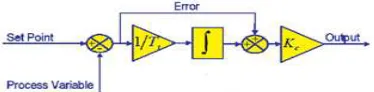
Proportional Response:
The difference between the set point and the process variable is called proportional component. This difference is referred to as the Error term. The ratio of output response to the error signal
determines the proportional gain (Kc). The control
system response increases with increasing proportional gain. If the proportional gain is too large, the process variable will begin to oscillate. If Kc is increased , the oscillations will get larger and the system will become unstable and may even oscillate out of control.
[image:3.595.84.271.533.579.2]
Figure.5.Block Diagram Of PI Control Algorithm
Integral Response: The integral component sums the error term slowly. The integral response will continually increase over time to drive the Steady-State error to zero. The difference between the process variable and set point is the final Steady-State error which is called integral windup. The integral action saturates a controller without the controller driving the error signal toward zero.
The PI controller output is equal to the control input to the plant, in the time-domain is as follows:
(2.6)
The PI controller transfer function is found by taking the Laplace transform of Equation(1).
(2.7) Kp=
Proportional gain = Integral gain The PI
controller transfer function is found by taking the Laplace transform of Equation(1).
3. SIMULATION RESULTS
The simulation is done using Matlab simulink and the results are presented here. The Open Loop IBC and Closed Loop IBC is shown in Fig.3.1 and Fig3.5. Input voltage of 220 V DC for Open and Closed Loop Circuit with disturbance at 0.04sec was shown in Fig.3.2 and 3.6. Output voltage of 48 V for Open and Closed Loop Circuit with disturbance was shown in Fig.3.3 and 3.7. Output current for Open and Closed Loop Circuit with disturbance was shown in Fig.3.4 and 3.8. When a sudden disturbance given to the input the closed loop circuit output voltage and current vary for a short time and settels down quickly compared to the open loop due to the presence of the controller in the circuit. Fig.3.9.shows the output ripple voltage of 0.012.
Figure3.1 Open Loop Buck Interleaved Converter Circuit With Disturbance.
Figure 3.3.Outputt Voltage For Open Loop Circuit With Disturbance.
Figure 3.4.Outputt Current For Open Loop Circuit With Disturbance.
Figure 3.5. Closed Loop Buck Interleaved Converter Circuit With Disturbance.
Figure 3.6.Input Voltage For Closed Loop Circuit With Disturbance.
Figure 3.7.Outputt Voltage For Open Loop Circuit With Disturbance.
Figure 3.8.Outputt Current For Closed Loop Circuit With Disturbance.
Figure 3.9.Outputt voltage ripple for pi with Open Loop Circuit.
4. EXPERIMENTAL RESULT
An Interleaved buck converter was built and tested for open loop and closed loop for 220VDC as input and output of 48Vdc.The hardware layout is shown in Figure 4.1.The hardware consists of power circuit and control circuit. The switching
pulse for M1and M2 are shown in Figure 4.2 and
4.3.The output voltage of 48V is shown in the CRO in Figure 4.4. The hardware is done using the ICs 89C2051, an computer hardware with software embedded called Embedded System an important component designed to perform a dedicated application, IR 2110,IRF840.The hardware is tested with resistive load with C-Filter and the results are presented here.
Figure 4.1. Hardware Snap Shot
Figure 4.2. Switching Pulse For M1(5v)
Figure 4.4.Output voltage (48v)
5.CONCLUSION
The Interleaved Buck Converter Open and Closed Loop is modeled and simulated using Matlab simulink. The results of simulation and hardware are presented in this paper. This converter has advantages like Zero voltage switching, improved step down ratio and reduced losses with a ripple of 0.012. The results of modified circuit was presented. The variation of output 48V DC with the variation with the input voltage 220V DC with disturbance was simulated. The simulation results are in line with the predictions.
REFERENCES
[1] P.L.Wong, P.Yang and F.C.Lee, Performance improvements of interleaving VRMs with coupling inductors, IEEE Trans. Power Electron 168 (2001), 499A507.
[2] R.L.Lin , C.C. Hsu , and S.K. Changchien , Interleaved four phase buck based current source with isolated energy recovery scheme for electrical discharge machine , IEEE Trans. Power electron, 24(2009), 2249A2258. [3] C. Garcia, P. Zumel, A.D. Castro, and J.A.
Cobos, Automotive DC to DC bidirectional converter made with many interleaved buck stages, IEEE Trans. Power electron., 21( 2006),578A 586.
[4] J.H. Lee, H.S Bac, and B . H. Cho, Resistive control for a photovoltaic battery charging system using a microcontroller , IEEE Trans. Ind Elec to iron , 55 (2008), no. 7, pp. 2767 to2775.
[5] Y.C. Chuang , High efficiency ZCS buck converter for rechargeable batteries, IEEE trans. Ind. Electron. 57, (2010) 2463A2472.
[6] C.S. Moo,Y.J.Cinen, H.L.Cheng, and
Y.C.Hiseh,Twin buck converter with Zero to voltage to transition,IEEE TRANS . IND. Electron. 58(2011) ,2366A237.
[7] X.Du and H.M.Tai,Double-frequency buck
converter, IEEE
Trans.Ind.Electron.,56(2009),1690A1698.
[8] K.Jin and X.Ryan, Zero-voltage-switching-multiresonant three-level converters, IEEE Trans. Ind. Electron., 54(2007), 1705A1715. [9] J.P.Rodrigues, S.A.Mussa, M.L.Heldwein, and
A.J.Perin,Three level ZVS active clamping PWM for the DC-DC buck converter,IEEE Trans.Power Electron.,24(2009),2249A2258. [10] X.Ruan, B.Li, Q.Chen, S.C.Tan, and
C.K.Tse,Fundamental considerations of
three-level DC-DC converters:
Topologies,analysis,and control,IEEE
Trans.Circuit Syst, 55(2008),3733A3743. [12] C.T.Tsai and C.L.Shen, Interleaved
soft-switching coupled-buck converter with active-clamp circuits, Proc.IEEE Int.Conf.Power
Electron. and Drive System.,
54(2009),1113A1118.
[13] J.Y.Lee, Y.S.Jeong, and B.M.Han, An isolated
DC/DC converter using high-frequency
unregulated LLC resonant converter for fuel
cell applications, IEEE
Trans.Ind.Electron.,58(2011),2926A2934. [14] M. Roslan, K. H. Ahmed, S. J. Finney, and
B.W.Williams, Improved instantaneous
average current-sharing control scheme for parallel-connected inverter considering line impedance impact in microgrid networks,
IEEETrans. Power