A Low-Voltage Single-Supply Level Converter for
Sub-VTH /Super-Sub-VTH Operation: 0.3V to 1.2V
Majid Moghaddam
Faculty of Electrical and Computing Engineering, Shahid
Beheshti University, G.C., Tehran, Iran
Mohammad Eshghi
Faculty of Electrical and Computing Engineering, Shahid
Beheshti University, G.C., Tehran, Iran
Mohammad Hossein Moaiyeri
Faculty of Electrical and Computing Engineering, Shahid
Beheshti University, G.C., Tehran, Iran
ABSTRACT
Digital sub-threshold circuits are significant for ultra-low power (ULP) applications. Operating circuits at ultra-low voltage levels leads to the less power per operation. An optimized method is separating the logic blocks based on performance requirement and utilizing multiple-supply voltage (VDD) for each blocks. In order to prevent an enormous static current in these multi-VDD circuits, voltage
level converters are required. The advantages of single-supply level converter (SSLC) over dual-supply level converter (DSLC) are on the grounds of pin count, congestion in supply routing, complexity and overall system cost. In this paper, a novel sub-threshold single-supply voltage level converter (S_SSLC) based on dynamically-controlled body biasing technique is presented. In this work, a dynamically-controlled body biasing is utilized for setting the threshold voltages of the transistors in order to reduce the delay. This dynamic design can convert an input signal at sub-threshold/super– threshold region ranging from 0.3v-1.2v to 1.2v as output. Simulation results at 180nm CMOS technology node demonstrate the superiority of the proposed design compared to the conventional SSLC designs.
Key Words: Digital sub-threshold circuits, ultra-low power, single-supply level converter, dynamically-controlled body biasing technique.
1. INTRODUCTION
ULTRA-LOW POWER systems include circuits that work in the sub-threshold region. Operation of sub-threshold circuits at ultra-low voltage (ULV) leads to considerably lower power consumption. Sub-threshold circuits need lower energy for the activity of transistors compared to circuits in strong inversion region. Nowadays, with regards to modern industry and expensive energy, power saving is very significant in most applications and circuits especially in the applications that do not need very high performance. For instance, the performance requirements for micro-sensor nodes are very low. Most micro-sensor node applications require very long battery lifetimes because it is not possible to recharge or replace batteries frequently.
Most portable electronics that are used for consumer applications require a low-power Digital Signal Processor (DSP) or Microcontroller Units (MCU). In order to provide lower power consumption, lowering the supply voltage (VDD)
leads to decrease dynamic power quadratically [1-5].
Low-power design methods comprise different levels such as system, register transfer logic (RTL), logic, circuit and device levels [6], [7]. There are some techniques such as reducing theswitching activity [8] or voltage scaling [9] for ultra-low power requirement of some portable application nodes, but these techniques are still almost inefficient. To overcome with this, digital sub-threshold logic is very helpful [8], [9]. Microprocessors, wireless sensor networks and some circuits that work with ultra-low voltage, require a level converter (LC) for communication with I/O circuits and other circuits that work at high-supply voltage. I/O circuits have to work at high supply voltage because of the needed noise-immunity. Even if we assume that there is no noise, by sending low-voltage signal from core logic and microsensor node to I/O circuits, when the signal state is logic ‘1’, the PMOS transistors in I/O circuits will not turn OFF completely and consequently the static current will increase.
In this work, a novel single-supply voltage level converter for sub-threshold logic based on the body biasing technique is proposed. The proposed sub-threshold single-supply level converter (S_SSLC) is appropriate for converting input signals from sub-threshold region, while other existing single-supply level converters are not practical at ULV. This S_SSLC by utilizing body biasing technique can convert input signal from 0.3v-1.2v to 1.2v. Moreover, the proposed LC consumes ultra- low power compared to other single-supply level converters. The advantages of SSLC over DSLC are on the grounds of pin count, congestion in supply routing, complexity and overall system cost [10].
The rest of the paper is organized as follows: In section 2, the related works are reviewed. In section 3, the proposed design is presented and section 4 contains the simulation results and discussion. Also, this section describes the temperature variation affect for operation of proposed LC as compared to conventional LC. Finally, section 5 concludes the paper. Section 6 shows references of the paper.
2. RELATED WORKS
Figure 1 and Figure 2 illustrate the conventional in [11] and SSLC design in [12]. Conventional and SSLC designs do not work in the sub-threshold region. This section discusses about conventional single-supply level converters and their problems in converting ultra-low voltages to required high-voltage.
Fig 1: Schematic of the conventional SSLC [11].
Fig 2: Schematic of the SSLC in [12].
When the input signal is ultra-low voltage, in the conventional LC in Figure 1, pull-down strength of M1 transistor is weak compared to strength of pull-up transistor (M2). Also, increasing the width (W) of M1 is not sufficient for a correct conversion. Furthermore, in this conventional LC, since the input signal has been connected to the gate of PMOS and NMOS transistors (M1, M2), in theultra-low-voltage input, M1 and M2 turn ON simultaneously, so the static current is increased. Utilizing the voltage doubler leads to increase the strength of the pull-down transistors [13], however, the boosting efficiency of the voltage doubler is substantially diminished in sub-threshold operation [14].
Also, in the SSLC of [12], shown in Figure 2, when the input signal (Vin) is logic ‘1’, the M5 transistor turns ON and the node “ob” is discharged. So, the node “VOUT” is charged to
VDDH. Since the node “ob” is discharged, M7 transistor
according to Figure 2 turns ON and a static current path is created from high-supply voltage (VDDH) to ground. Therefore, power consumption is increased. Figure 3(a) explains the level conversion steps of the SSLC in [12]. M5 transistor pulls down the node “ob”, when the input voltage signal is changed to logic ‘1’, resulting in turning M3 transistor ON. It should be noted that both up and pull-down transistors (M5 and M4) turn ON simultaneously in step 1 of Figure 3(a). For discharging node “ob,” the flowing drive-current through M5 should be larger than the flowing current through M4. If both M5 and M4 operate under comparable gate-source voltage (|VGS|), this demanded can be easily compensated by suitably sizing the transistors. However, when the input signal is in the sub-threshold region, the drive current of M5 transistor decreases exponentially as
(a)
(b)
Fig 3: Failure mechanism of the SSLC of [12] when ultra-low voltage input is applied. (a) Level conversion steps of SSLC. (b) Level conversion fails in ultra-low voltage input due to weak pull down.
the gate voltage is diminished. Therefore, the pull-down strength of M5 that has sub-threshold input signal is very weak compared to pull-up strength of M4 that has high-voltage input signal. Furthermore, in such a condition, device sizing techniques are unpractical to provide strong pull-down enough for level conversion. Hence, it fails to discharge node “ob” as shown in Figure 3(b). Therefore, the SSLC of [12] is impractical in sub-threshold region. Furthermore, in this design, according to Figure 2, a reverse current flows when the input signals are lower than 70% of VDDH (i.e. Vin=0.85V when VDDH=1.2V). As a result, SSLC design in [12] is not low-voltage and suitable for ultra-low power applications. In the next section, a novel single-supply voltage LC is proposed that can work at low voltages.
3. THE PROPOSED LC STRUCTURE
Conventional level converters are impractical to communicate as interface between sub-threshold logic and I/O circuit. The proposed sub-threshold single-supply level converter (S_SSLC) is shown in Figure 4. It is able to convert sub-threshold input signals to the high-voltage level (VDDH) as output.
BS BSn DS DSn TH
THn
V
V
V
V
0
(1)BS BSp DS DSp TH
THp
V
V
V
V
0
(2)For converting sub-threshold input signal to 1.2v as output, the strength of input transistor (M2) must overcome M6 transistor. To this end, the proposed design utilizes dynamic control body-biasing for increasing the strength of input transistor (M2) byconnecting its bulk to Vin-low (see Figure 4). Also, the bulk of all PMOS transistors is connected to VDDH in order to increase their threshold voltage (VTHp) according to Eq. (2). This is helpful for weakening M6 transistor and increasing the strength of M2 transistor. When the Vin-low is logic ‘1’, the body-source voltage (VBS) for
M2 is increased, so according to (1), the VTHn is reduced. Therefore, the proposed S_SSLC could convert input signal from 0.3V to 1.2V.
The proposed S_SSLC has two main stages. The first stage utilizes diode-connected NMOS (M7) to enable dependable conversion across variation and temperature with ultra-low voltage input signal. The second stage is a cross-coupled differential inverter (M8-M11), which convertsthe output of the first stage from 0, VDDH-VTH to full voltage swing (0, VDDH) as final output (VOUT). Threshold voltage (VTH) and the size of transistors for proposed design can be briefly described as follows:
[image:3.595.43.280.435.612.2]TheVTHof NMOS and PMOS transistors are set for correct conversion. According to Figure 4, when input signal is logic ‘0’, M1 turns ON then M6 turns ON, leading to turning ON M8. So the output node through M8 is discharged to ground. Therefore, there is no problem for level converter. When input
Fig 4: Schematic of the proposed S_SSLC.
Table 1: Simulation results at VDDH =1.2 v.
Level Converter
Vin- low (V)
Total Power
(nW)
Average Delay
(ns)
EC 1 (fJ)
Static Power (nW)
Proposed 0.4 565.1 10.1 5.7 1.24
Conventional 0.4 892.7 35.8 31.95 1.37
1
EC: Energy Consumption
signal is logic ‘1’, the input transistor (M2) should overcome M6 to pull down the input node of M8 and help to turn ON M5 for charging the output node. Since M2 has a sub-threshold input, the bulk of M2 is connected to input signal
(Vin-low) to decrease its VTH when input signal is logic ‘1’.
Also, the bulk of all PMOS transistors are connected to VDDH
with this purpose to increase their VTH according to (2). Furthermore, in the proposed S_SSLC, NMOS diode-connected transistor (M7) is utilized to increase M2 ability as compared to M6. Thus, proposed S_SSLC could perform at sub-threshold regime.
The higher VTH will reduce the switching power and consequently, the static power is reduced by decreasing the leakage current of OFF transistors [1]. Low gate capacitance
(Cg) in weak inversion leads to switching power reduction
[16]. In the proposed design, the size of all PMOS and NMOS transistors except M10 and M11 are chosen to the minimum technology size (180 nm: 400 nm). The length (L) of M10 and M11 are different. Since utilizing body-biasing by connecting the body of all PMOS to VDDHand using auto dynamically- controlled body-biasing for M2 is enough to increase the its strength and provide correct conversion. Furthermore, using diode-connected NMOS (M7) creates a voltage drop (VTHn) for supply voltage of the stage one and helps to increase the capability for converting low-voltage inputs. In other words, the diode-voltage drop across M7 leads to more increasing VTHp for M5 , M6 and M3. Also, increasing the length of the M10 and M11 (LM10=LM11= 360 nm) in the second stage of the proposed design ensured that the strength of M8 and M9 is increased, since the input signal of M8 and M9 in the second stage is over the sub-threshold range. The properties of the proposed S_SSLC can be expressed briefly as follows: 1. Designing a novel SSLC structure.
2. Practical in converting sub-threshold input signals. 3. Utilizing body biasing and suitable setting the size of the transistors, in order to increase the efficiency and performance.
4. Decreasing the pin count, congestion in supply routing, complexity and overall system cost.
4. SIMULATION RESULTS AND
DISCUSSION
In this section, the simulation results of the proposed design and comparison with other existing single-supply level converters are presented. For this purpose, each cell is optimized and simulated at 180 nm bulk CMOS technology node using Cadence Virtuoso tool.
consumption (EC, power × delay) and specifically less leakage power consumption. Furthermore, the proposed design also converts 0.3V input signal, consequently it is low-voltage and low-power.
Figure 5 shows that the proposed LC successfully converts 0.4V input signal to 1.2V
Figure 6 illustrates the delay simulation of the proposed design versus input signal for converting the input signal from Vin-low to Vout at 1.2VVDDH.
The Proposed S_SSLC for an input signal between 0.3V-0.4V, adds less than 25 ns delay, however, these delays are appropriate for many sub-threshold applications [17-19]. Utilizing M7 as a diode-connected in the first stage of the proposed LC leads to a VTHn voltage drop for supply voltage of the first stage. Therefore, theVDDHis not static during the transition time [1]. Also, the bulk of input transistor (M2) is connected to input signal (Vin-Low) in order to create dynamically-controlled body biasing. Furthermore, the bulk of all PMOS transistors are connected to VDDH.
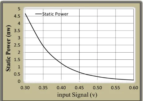
[image:4.595.318.549.73.237.2] [image:4.595.318.553.272.446.2]These proposed techniques are helpful for weakening PMOS transistors (M3 and M6) compared to NMOS transistor (M2). Because, NMOS transistor (M2) has low-voltage input signals (Vin-Low). The higher VTH will reduce the utilized energy during the transition time and also the leakage current of OFF devices is reduced. Thus, the power consumption of the proposed S_SSLC is reduced. The static and total power results of the proposed S_SSLC are shown in the Figure 7 and Figure 8.
Fig 5: waveforms of the proposed level converter. Vin- low = 0.4V at 10MHZ and VDDH = 1.2 V.
Fig 6: Delay simulation of proposed LC for a conversion from Vin-low to Vout at 1.2 v single supply voltage (VDDH).
Fig 7: Static power dissipation versus input signal for Proposed LC at 1.2 v single supply voltage (VDDH).
Fig 8: Total power simulation versus input signal for proposed LC at 0.4V, 10MHZ input signal (Vin- low) and VDDH = 1.2 V. Minimum power point is occurred between ranging 0.35 to 0.4 V.
As the input signal is increased, static current through M3 is reduced. Minimum power point (MPP) for proposed design is occurred between 0.35V and 0.4V, so the proposed design is suitable for low-voltage applications.
4.1
Temperature Variations Effects
The temperature variation may considerably influence the characteristics of the sub-threshold LC. These variations may affect the threshold voltage and sub-threshold swing. The conventional LC is not functional at lower than 0.4 V input signal. So, the effect of temperature variations on the proposed design and conventional design for 0.4 V input signal is investigated.
[image:4.595.50.282.381.540.2] [image:4.595.50.279.574.732.2]Fig 9: Simulated results of total power versus temperature variation for proposed design and conventional design at 0.4V, 5MHZ input signal and VDDH=1.2V.
5. CONCLUSION
In this paper, a novel single-supply voltage level converter has been presented. This design was significant for decreasing the supply routing, complexity and overall system cost. It was simulated in 180 nm bulk CMOS technology. In this proposed design also, dynamically-controlled body-biasingwas utilized
for input NMOS transistor that has low-voltage inputs to decrease its threshold voltage. Furthermore, the bulk of all PMOS transistors were connected to VDDHto increase their threshold voltage. As a result, the proposed design could convert sub-threshold input signal to 1.2V as output. The proposed design successfully and reliably up-converted the input signal voltage ranging 0.3V to 1.2V into 1.2V. Therefore, it was appropriate for sub-threshold applications. Also, the minimum power point (MPP) for the proposed design was near the 0.4V supply voltage. Other existing single-supply level converters were not low-voltage and practical for converting the sub-threshold input signals. SSLC in [12] was non-functional at input-signal voltage lower than 0.85V. Also, the conventional design was non-functional at input lower than 0.4V. The EC (Energy Consumption) for our proposed design was 83% lower than conventional LC. Furthermore, the proposed design was robust against temperature variation.
6. REFERENCES
[1] S. N. Wooters, B. H. Calhoun and T. N. Blalock “An Energy-Efficient Subthreshold LevelConverter in 130-nm CMOS,” IEEE Trans. Circuits Syst. II, Exp. Briefs, vol. 57, no. 4, pp. 290 – 294, Apr. 2010.
[2] A. Wang, A. Chandrakasan, and S. Kosonocky, “Optimal supply and threshold scaling for subthreshold CMOS circuits,” in Proc. IEEE Comput. Soc. Annu. Symp. VLSI, 2002, pp. 5–9.
[3] I. J. Chang, J.-J. Kim, and K. Roy, “Robust Level Converter for Sub-Threshold/Super-Threshold Operation: 100 mV to 2.5 V,” IEEE Trans. Very Large Scale Integr. (VLSI) Syst, vol. 19, no. 8, pp. 1429 – 1437, Aug. 2011.
[4] H. Soeleman and K. Roy, “Ultra-low power digital subthreshold logic circuits,” in Proc. ISPLED, 1999, pp. 94–96.
[5] A. Wang, B. H. Calhoun, A. P. Chandrakasan, Sub-threshold Design for Ultra Low-Power Systems, 233 Spring Street, New York, NY 10013, USA, 2006. [6] K. Navi, M. H. Moaiyeri, R. Faghih Mirzaee, O.
Hashemipour, and B. Mazloom Nezhad, “Two new low-power full adders based on majority-not gates,” Elsevier, Microelectronics Journal, Vol. 40, No. 1, pp. 126-130, Jan. 2009.
[7] M. H. Moaiyeri, R. Faghih Mirzaee, K. Navi, T. Nikoubin, and O. Kavehei, “Novel Direct Designs for 3-Input XOR Function for Low Power and High-Speed Applications,” Taylor and Francis, International Journal of Electronics, Vol. 97, No. 6, pp. 647-662, Jun. 2010. [8] A. Wang and A. Chandrakasan, “A 180-mV subthreshold
FFT pro-cessor using a minimum energy design methodology,” IEEE J.Solid-State Circuits, vol. 40, no. 1, pp. 310–319, Jan. 2005.
[9] H. Soeleman and K. Roy, “Ultra-low power digital subthreshold logic circuits,” in Proc. Int. Symp. Low Power Electron. Des. (ISLPED), 1999, pp. 94–96. [10] Q. A. Khan, S. K. Wadhwa and K. Misri., “A Single
Supply Level Shifter for Multi-Voltage Systems,” 19th Internation Conference on VLSI Design, pp. 557-560, 2006.
[11]R. Puri, L. Stok, J. Cohn, D. S. Kung, D. Z. Pan, D. Sylvester, A. Srivastava, S. Kulkarni, “Pushing ASIC Performance in a Power Envelope,” DAC-40: ACM/IEEE Design Automation Conference, pp. 788-793, Anaheim, CA, June. 2003.
[12]J. Y. An, H. S. Park and Y. H. Kim, “Level Up/Down Converter with Single Power-Supply Voltage for Multi-VDD Systems,” the semiconductor technology and science journal, vol.10, no.1, March, 2010.
[13]A. Chavan, E. M. Donald, Electrical and Computer Engineering Department, University of Texas at El Paso IEEEAC paper 2007.
[14]J. Kil, J. Gu, and C. Kim, “A high-speed variation-tolerant interconnect technique for sub-threshold circuits using capacitive boosting,” IEEE Trans. Very Large Scale Integr. (VLSI) Syst., vol. 16, no. 4, pp. 456–465, Apr. 2008.
[15]S. Narendra, V. De, S. Borkar, D. Antoniadis, and A. Chandrakasan, “Full-chip subthreshold leakage power prediction and reduction techniques for sub-0.18µm CMOS,”IEEE J. Solid-State Circuits, vol. 39, no. 3, pp. 501–510, Mar. 2004.
[16]Y. Taur and T. H. Ning, Fundamentals of Modern VLSI Devices. Cambridge, U.K.: Cambridge Univ. Press, 1998.
[17]B. Zhai, S. Pant, L. Nazhandali, S. Hanson, J. Olson, A. Reeves, M. Minuth, R. Helfand, T. Austin, D. Sylvester, and D. Blaauw, “Energy-efficient subthreshold processor design,” IEEE Trans. Very Large Scale Integr. (VLSI) Syst., vol. 17, no. 8, pp. 1127–1137, Aug. 2009.
[18]J. Kwong, Y. Ramadass, N. Verma, and A. Chandrakasan, “A 65 nm sub-vt microcontroller with integrated SRAM and switched capacitor DC–DC converter,” IEEE J. Solid-State Circuits, vol. 44, no. 1, pp. 115–126, Jan. 2009.
![Fig 2: Schematic of the SSLC in [12].](https://thumb-us.123doks.com/thumbv2/123dok_us/8076947.781170/2.595.314.549.74.398/fig-schematic-sslc.webp)