International Journal of Emerging Technology and Advanced Engineering
Website: www.ijetae.com (ISSN 2250-2459, ISO 9001:2008 Certified Journal, Volume 8, Issue 2, February 2018)
117
Implementation of Optical Exor & Exnor Operation Using
Multiplexer
Kamal K. Upadhyay
Department of Electronics & Communication, University of Allahabad, India
Abstract—As the receiving end of an optical network opto electronics conversion of data takes place for the processing purpose. Electronic processing of high speed data dissipates huge amount of heat energy. this heat is directly proportional to the elements which are used in any circuit . huge numbers are elements used in any circuit design it means no huge amount of heat dissipation. This problem can be solved by reducing the number of element in the same circuit. In this proposed model the above said problem can be reduced.
Keywords— Multiplexers(mux), Optical logic gate, cross phase modulation(XPM), cross gain modulation(XGM).
I. INTRODUCTION
In the present society where we live is full of digital equipments wherever we see, as we are living and experiencing the information era. In today’s world huge amount of data is being generated, transported and processed. Optical fiber is the medium used for transportation of data at very high rate. For electronics processing, opto-electronic conversion of data takes place at the receiving end high data rate signal processing result in increased consumption of power and heat generation from electronic integrated circuit. It is stated in few papers (notomi et al.2011)[1]; Shancham et al.(2008)[2] that even the electronic transportation of high speed data among the processing nodes consumes major chunk of energy. These are the limiting factors in expanding high speed data networking and processing. If data is being transported in optical domain it should also be processed in optical domain and hence the elimination of opto electronic conversion and development of all optical processing is need of the hour. The main advantage of all optical data processing is its high data rate, low power consumption and fast dynamics. Optical logic gates are building blocks of the photonic processing circuits. In recent years extensive research has been done in designing of all optical logic gates like AND (Li et. Al. 2009)[3] OR(Singh et al.
2014)[4], NOT (Singh et al. 2013)[5], NAND (Mohammadnejad et. Al. 2009) [6] and NOR (Hamie et.
Al. 2002)[7].
[image:1.612.339.539.284.380.2]
But all of the them used near about similar design to implement and no one try to reduced the circuit elements. In the proposed model we used multiplexer to design the logic gate ( EXOR , EXNOR). In the current paper a novel design of 2 derived logical operations.
Fig. 1 Symbolic diagram of EXOR and EXNOR gates
EXOR and EXNOR which will save space if incorporated in more complex circuits. And also reduced the problem of heat dissipation, because more heat dissipation can harm the integrated circuit. A multiplexer is a kind of digital circuit having n input and one output known as n:1 multiplexer, also known as many to one circuit. It has 2^n- input mux has n select lines. Fig 1 shows
the basic symbolic diagram of the proposed model
.
II. PRINCIPLE OF OPERATION AND MODEL FORMULATION
In the proposed model the logical operation EXOR and EXNOR are achieved with the help of Multiplexer. The red line shows the input data A while the representation of data B is by green colour other than these two input A ,B data all zero and All one are shows by Input data 0 and input data 1 respectively. In fig 2 the block diagram of proposed model is designed here data A is given in select line of multiplexer and input 1 is given as first input of multiplexer and input zero given to second input of multiplexer output comes from here gives which is further input as second arm of multiplexer 2 while in first arm of mux 2 input B is given which combine in multiplexer. Multiplexer process
the input data and gives the output P which is B output
International Journal of Emerging Technology and Advanced Engineering
Website: www.ijetae.com (ISSN 2250-2459, ISO 9001:2008 Certified Journal, Volume 8, Issue 2, February 2018)
118
[image:2.612.336.550.154.366.2]Similarly the output of mux 1 given to first arm to the multiplexer 3 and in the second arm of multiplexer 3 is data B given as input both the data processed by multiplexer and gives the output Q i.e which is standard form of EXNOR gate.
[image:2.612.68.266.221.603.2]Fig. 2 block diagram of proposed model
TABLE 1.
FUNCTIONAL TABLE FOR EXOR GATE
Serial no.
INPUT DATA
A
INPUT DATA
B
OUTPUT
P= B
1. 0
0 0
2. 0
1 1
3. 1
0 1
4. 1
1 0
TABLE 2.
FUNCTIONAL TABLE FOR EXNOR GATE
Serial no.
INPUT DATA
A
INPUT DATA
B
OUTPUT
Q=
1. 0
0 1
2. 0
1 0
3. 1
0 0
4. 1
1 1
Formulation
Here A and B are inputs having data values (0011) and (0101) repectively
When data B is given as select lines of MUX 1. The mux process is described as follow.
INTERMIDIATE RESULT FROM
MUX 1 = 1x + 0xB
=
This result given as input for mux 2 and data B works here as select line. MUX 2 processed as follow and gives the result X as output.
P = Bx + xA
P = B+A
P = A
Above output P verified by standard result
Similarly,
International Journal of Emerging Technology and Advanced Engineering
Website: www.ijetae.com (ISSN 2250-2459, ISO 9001:2008 Certified Journal, Volume 8, Issue 2, February 2018)
119
Q = x +AxB
Q = +AB
Q = A
Above output Q verified By standard result of Output of EXNOR gate.
III. THEORITICAL ANALYSIS
The Refractive index of the active region of a SOA is determined by the carrier density N of SOA, so pump signal propagating through the active region of SOA decreases its carrier density [8] and modulates the refractive index which in turn gives rise to phase modulation of the probe beam. Similarly XGM also takes place due to gain saturation of SOA. The dynamics of SOA are:
= -R(N)-Vg.g(N).Nph ----(1)
G(N) = (N-N0) ----(2)
Where N is the carrier density , J is the injection current density, R(N) is the recombination rate, Vg is the group
velocity of light , g(N) is the material gain coefficient, Nph
is photon density, e is the electron charge, d is the active layer thickness and Nph is photon density. Γ is the
confinement factor 𝛔g is the differential gain, V is the
volume of the active region of SOA and N0 is the carrier
density for transparency. Gain per unit length of SOA is written as:
G =ℾ.g(N)–α --- (3)
Where α is the total loss coefficient per unit length. The overall gain for entire length of SOA increases exponentially and is described as:
Gs = eg.L ----(4)
Where L is the length of the active region of SOA.
Here in this proposed design all the inputs signal(pump,probe1,probe2) are generated through mode lock laser (MLL) . Mode lock laser generate a Gaussian pulse. If u(t) represents a Gaussian field amplitude.
(5)
Where t0 is pulse width and TFWHM is the full width at
half maximum (singh et al. 2015)[9]
The input of the external mach-zehnder type modulator is optical Gaussian pulse the insertion loss is 5 dB and chirp factor is 0.5. this chirp factor induces phase change. It is calculated as:
= (7)
Where c is the chirp factor, s is the intensity of light and Ø is an optical instantaneous phase of incoming light. Binary input sequences (A, B, C, probe1, probe 2) are generated by PRBS( pseudo random bit sequence ) generator. This binary sequence is then fed in to electrical generator. The raised cosine pulse represents a binary bit which is generated by electrical signal generator.
(8)
In above equation Amax represents the maximum value of
the output electrical signal representing a binary number 1, TB is a binary bit period and α represents the pulse width
parameter. Through mach-zehnder modulator the electrical raised cosine pulse modulates the optical Gaussian pulse. Hence the refractive index changes due to change in carrier density N of the active region of SOA. Following equation represents the dynamics of SOA ( Bass et al.2001 )[10].
(9)
Where N is the carrier density, R(N) is recombination rate ,d is the thickness of the active region, e represents charge on electron. Nph denotes photon density , J is
injection current density and group velocity of light is represented by vg. g(N) shows gain coefficient of material.
(10)
where⎾ shows the confinement factor, volume of active region represented by V and σg denotes the differential
gain.
(11)
Above equation represents the net gain (Singh et al. 2015). Where α is the loss coefficient. The total gain is calculated at the location las :
(12)
To find the average power ( Pav(N,T)) is integration of
International Journal of Emerging Technology and Advanced Engineering
Website: www.ijetae.com (ISSN 2250-2459, ISO 9001:2008 Certified Journal, Volume 8, Issue 2, February 2018)
120
(13)
(14)
(15)
The power of SOA for length L can be written as
(16)
Therefore
(17)
(18)
Equation 14 denotes the change in the carrier density changes the phase of the signal. Where αEF is the line width
enhancement factor.
IV. RESULT AND DISCUSSION
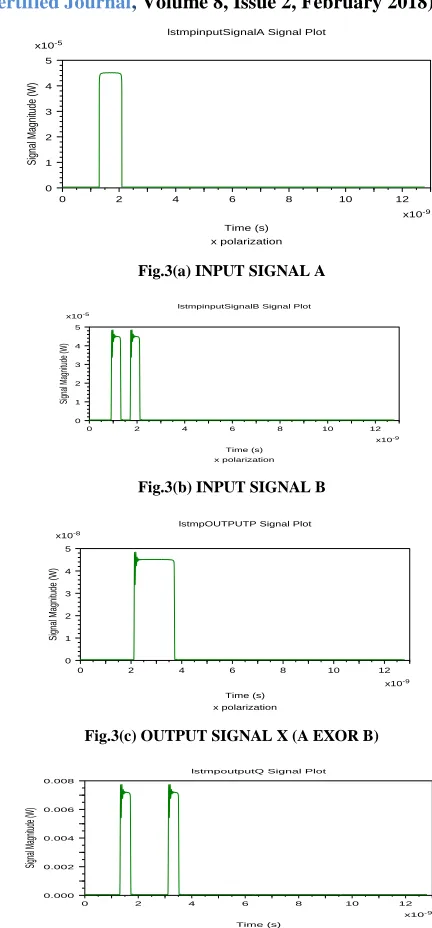
The proposed design of photonic circuit works at 10 Gbps data rate. All three Mux’s used in this design have similar values Fig. 3a-b represents the input signals, and the output signals represented by fig. 3c and 3d. P is the EXOR of inputs A and B. and it is verified by truth table Table1. Fig. 3c shows the output signal P. Fig 3d shows the output of EXNOR for the Input A and Input value B and verified by the truth table of EXNOR gate which is presented by table 2The output signals shown here are actually the low power probe signals which are the inverted copy of their high power pump signals after passing through SOA. Therefore these overshoots occur for the rising edge of the high power pump signal which corresponds to falling edge of probe signal for the same instance of time. Both rising edge of the pump signal as well as the falling edge of the probe signal experiences high gain due to the presence of high population of carriers for that period of time. One of the reasons for high population of carrier for that particular time period is the absence of high power pump signal just before the overshoot. The overshoot is actually instigated by the high power signal.
lstmpinputSignalA Signal Plot
x polarization
x10-9
Time (s)
0 2 4 6 8 10 12
x10-5
S
ig
na
l M
ag
ni
tu
de
(W
)
0 1 2 3 4 5
Fig.3(a) INPUT SIGNAL A
lstmpinputSignalB Signal Plot
x polarization
x10-9
Time (s)
0 2 4 6 8 10 12
x10-5
Si
gn
al
M
ag
ni
tu
de
(W
)
0 1 2 3 4 5
Fig.3(b) INPUT SIGNAL B
lstmpOUTPUTP Signal Plot
x polarization
x10-9
Time (s)
0 2 4 6 8 10 12
x10-8
S
ig
na
l M
ag
ni
tu
de
(W
)
0 1 2 3 4 5
Fig.3(c) OUTPUT SIGNAL X (A EXOR B)
lstmpoutputQ Signal Plot
x10-9
Time (s)
0 2 4 6 8 10 12
Sig
na
l M
ag
nit
ud
e (
W
)
0.000 0.002 0.004 0.006 0.008
[image:4.612.49.273.122.301.2] [image:4.612.328.544.124.588.2]International Journal of Emerging Technology and Advanced Engineering
Website: www.ijetae.com (ISSN 2250-2459, ISO 9001:2008 Certified Journal, Volume 8, Issue 2, February 2018)
121
To evaluate the performance of the incorporated logic gates the extinction ratio and the quality factor for various lengths of active region of SOA and confinement factor of SOA are plotted. Extinction ratio is the ratio of two optical powers, power of bit 1 to the power of bit 0. For an efficient optical system the power gap between 1 and 0 should be large enough to facilitate the correct identification of the obtained bit. Therefore higher value of ER denotes better system performance. Extinction ratio is defined as the ratio of minimum output peak power of bit 1 to the maximum peak output power of bit 0 (Chattopadhyay 2011)[11].
V. CONCLUSION
An implementation of EXOR and EXNOR optical gates in a single photonic circuit is done success-fully in this manuscript. Multiple optical gates onto a single chip will lead to optical signal processing in the future and electronic circuitry will be replaced by the optical circuitry. With the development of photonic circuitry it is now possible to get any digital result in optical domain. The very basic two input one output optical line selector can be integrated to form a part of more bigger and complex photonic circuit. Development of photonic circuits like these are leading towards all optical signal processing which is the ultimate goal.
REFERENCES
[1] Notomi, M., Shainya, A., Nozaki, K., Tanabe, T., Matsuo, S., Kuramoch, E., Sato, T., Tanyama, H., Sumikura, H.: Low power nanophotonic devices based on photonic crystals towards dense photonic network on chip. IET Circ. Device Syst. 5, 84–93 (2011).
[2] Shancham, A., Bergman, K., Carloni, L.P.: Photonic networks-on-chip for future generation of networks-on-chip mul-tiprocessors. IEEE T. Comput. 57, 1246–1260 (2008)
[3] Shancham, A., Bergman, K., Carloni, L.P.: Photonic networks-on-chip for future generation of networks-on-chip mul-tiprocessors. IEEE T. Comput. 57, 1246–1260 (2008)
[4] Singh, P., Dixit, H.K., Tripathi, D.K., Mehra, R.: Design and analysis of all optical inverter using SOA-based mach-zehnder interferometer. Optik 124, 1926–1929 (2013).
[5] Singh, P., Tripathi, D.K., Jaiswal, S., Dixit, H.K.: Design of all optical buffer and OR gate using SOA-MZI. Opt. Quant. Electron. 46, 1435–1444 (2014).Bowman, M., Debray, S. K., and Peterson, L. L. 1993. Reasoning about naming systems. .
[6] Mohammadnejad, S., Chaykandi, Z.F., Bahram, A.: MMI-based simultaneous all optical XOR-EXOR-Or and XEXNOR-NOT multilogic gate for phase based signal. IEEE J. Quantum Elect. 50, 1014–1018 (2014)
[7] Hamie, A., Sharaiha, A., Guegan, M., Pucel, B.: All optical logic EXNOR gate using two cascade semicon-ductor optical amplifiers. IEEE Photonic Tech. L. 14, 1439–1441 (2002).
[8] Kumar, A., Kumar, S., Raghuwanshi, S.K. :Implementation of full adder and full subtractor based on electroopto effect in Mach-zehnder interferometers. Opt.Commun., 324 ( 2014).
[9] Song, H.J., Lee, J.S., Song, J.I.: Single up conversion by using a cross phase modulation in all optical SOA-MZI wavelength converter. IEEE Photonic. Tech. L. 16, 593–595 (2004).
[10] Bass, M., Enoch, J.M., Stryland, E.W.V., Wolfe, W.L.: Handbook of Optics. McGraw-Hill, USA (2001).