N A N O E X P R E S S
Open Access
Automatic hammering of nano-patterns on
special polymer film by using a vibrating AFM tip
Xiaodong Hong
1*, Yongkang Yang
2and You Wang
2,3*Abstract
Complicated nano-patterns with linewidth less than 18 nm can be automatically hammered by using atomic force microscopy (AFM) tip in tapping mode with high speed. In this study, the special sample was thin
poly(styrene-ethylene/butylenes-styrene) (SEBS) block copolymer film with hexagonal spherical microstructures. An ordinary silicon tip was used as a nano-hammer, and the entire hammering process is controlled by a computer program. Experimental results demonstrate that such structure-tailored thin films enable AFM tip hammering to be performed on their surfaces. Both imprinted and embossed nano-patterns can be generated by using a vibrating tip with a larger tapping load and by using a predefined program to control the route of tip movement as it passes over the sample’s surface. Specific details for the fabrication of structure-tailored SEBS film and the theory for auto-hammering patterns were presented in detail.
Keywords:Automatic nanolithography, Atomic force microscopy, Poly(styrene-ethylene/butylenes-styrene)
Background
Nano-sized patterns can be created on sample surface using a variety of different surface modification techniques. As a complement to conventional photo and electron-beam lith-ography, atomic force microscopy (AFM) nanolithography appears to be a unique tool with nanometer accuracy. High resolution AFM nanolithography also provides the ability to create various specialized site-specific nano-patterns or localized functional surface structures; with the integration of additional measurement modules, it allows for the phys-ical and morphologphys-ical qualities of surface undulations to be immediately characterized. This combined fabrication and characterization function in AFM nanolithography allows convenientin situ and in-line pattern creation and characterization [1-6].
There are many AFM nanolithography techniques for surface modification. Some techniques rely on mechanical (contact) interactions between the probe and the sample [6-9]. Various hard or soft materials can be directly removed by the typical mechanical [9,10] or thermomecha-nical [11] scratching technique. In this field, soft polymer
materials are widely used as masking or resisting materials in the fabrication of many devices, and polymer films have been also used to create patterns in their surfaces by an AFM tip with a radius of about 10 nm [12,13]. Sohn and Willett [14] described a novel technique for plowing pat-terns in masks or resistance material on an arbitrary sub-strate, in which material can then be deposited for the fabrication of metallic nanostructures. Cappella and Sturm presented a dynamic plowing nanolithography method (DPL) [15-17]. In their method, surface modification oc-curred through plastic deformation of the material surface after being plowed by a vibrating tip. They also compared DPL with indentation by means of force displacement curves; results showed that the border walls surrounding the lithographed structures using DPL method were much bigger than those created through indentation. Another branch of AFM nanolithography involves the flow of elec-trical current between the probe (or tip) and the sample. In this field, local oxidation of silicon surfaces is used as a very promising lithographic method by which to create a modi-fied surface at a nanometer scale. Garcia et al. [6] studied the effects and results for the reproducibility, voltage de-pendence, and kinetics for when oxidation occurred by using dynamic force microscopy modes. In another study involving electrical current and oxidation, Perez-Murano et al. [7] adopted a local oxidation method to grow silicon * Correspondence:[email protected];[email protected]
1
College of Materials Science and Engineering, Liaoning Technical University, Fuxin 123000, China
2
Materials Physics and Chemistry Department, Harbin Institute of Technology, Harbin 150001, China
Full list of author information is available at the end of the article
nanostructure [18] are suitable for hammering nano-patterns in their surfaces by using vibrating AFM tip manually. In the tailored SEBS films, hexagonal-spherical polystyrene (PS) plastic microdomains are embedded in poly(ethylene/butylenes) (PEB) rubber matrix. When the PS microdomain arrays are selectively indented by AFM tip hamming under hard tapping conditions, either imprinted or embossed patterns can be generated. The complete process is documented in our paper titled‘AFM tip hammering nanolithography’ (ATHN) [19]. However, manual AFM tip hammering lithography has some rough qualities and restrictive limitations: it is a slow, tedious and complicated nanolithography method and prone to error, which limits its promise in potential applications. Based on our studies in ATHN, an improved AFM tip hammering nanolithography method is proposed in this article. The method improves upon the capabilities for AFM tip hammering via a different process, which results in improving the hammering speed and precision greatly. Complicated nano-patterns can now be hammered out by using automatic methods in accordance with the prepro-grammed routes. The system allows for high-speed, high resolution, and exact duplication in the hammering of various complicated nano-patterns on tailored SEBS film surfaces. The specifics for the method, the process and examples are presented in the following work.
Methods
Materials
Poly(styrene-ethylene/butylenes styrene) triblock copoly-mer, coded as Kraton G1650, manufactured by Shell Co. (Shell Oil Co., Houston, TX, USA), with PS’s molecular
weight of 10,300 g/mol and PEB’s of 53,300 g/mol,
polydispersity of 1.19, and polystyrene content of 29 wt.%. Xylene and cyclohexane were used as supplied from TEDIA Co. Ltd. (Fairfield, OH, USA).
Preparation of sample films
The powder of SEBS G1650 was dissolved in xylene to form a solution with concentration of 0.3 wt.%. After drop-casing the solution onto freshly cleaved mica surface, monolayer SEBS films of 35 nm thick were prepared. The film thick-ness was measured using an AFM tip scratch technique that we previously developed, and the detailed description of the measurement procedure is given elsewhere [20].
necessary according to the judgment of naked eyes in the whole solvent vapor annealing process. The sample was annealed for about 40 h.
Equipment and software
A MultiMode NanoScope IIIa SPM (Veeco Instruments, Plainview, NY, USA) and a commercial probe NSG 10 (NT-MDT Company, Zelenograd, Moscow, Russia) with a force constant of 5.5 to 22.5 N/m were used, and resonant frequency of tip was around 255 kHz. Nanolitho-graphy software version 5.12 [21] was used for automatic-ally controlling the predefined routes in the hammering of the nano-patterns, and Microsoft Visual C++ Compiler (Microsoft Corporation, Shanghai, China) was needed to write the program.
Results and discussion
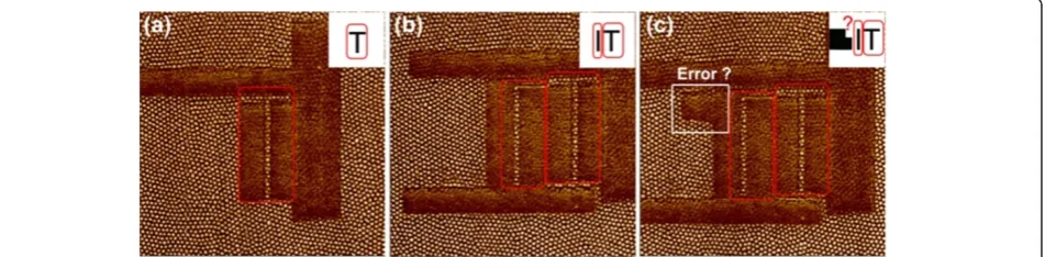
Shown in Figure 1a is AFM phase image of the as-cast morphology of a 35-nm thick SEBS G1650 thin film pre-pared from solution in xylene. The brighter domains in AFM phase images correspond to PS phase. It can be seen from Figure 1b that after being annealed in cyclo-hexane vapor for about 40 h, the poorly ordered PS cylinders have transformed into well-ordered hexagonal PS spheres. Using structure-tailored monolayer SEBS thin film as media, ATHN [19] was developed. An oscil-lating AFM tip in tapping mode was used as a nano-hammer forging the special sample surface to ‘write’ ei-ther imprinted or embossed patterns with a sub-20-nm linewidth resolution. Figure 1c shows an embossed letter ‘H’pattern made up of a single array of PS spheres with a diameter of 20 nm, which was generated by ATHN using manual procedure.
in the same way. Figure 2c shows an obvious fault in the attempted hammering of the letter ‘H’ character. The error means the failure of manual writing the embossed pattern-word HIT. The failed hammering process high-lights obvious shortcomings and drawbacks with ATHN manual procedure, such as complicated operation, low efficiency, and error-prone.
In order to overcome these problems, an improved automatic system for the hammering of complex nano-patterns is proposed on the basis of Nanolithography Software 5.12 [21]. Next, nanolithography software was introduced simply. The nanolithography feature allows for the performing tip moving in nanometer accuracy. Lithography programs direct the microscope for inscrib-ing or movinscrib-ing items on a sample surface. Nanolithogra-phy is achieved by using a tip as a hammering tool to create nano-patterns on the sample surface. Microsoft C programming language, along with NanoScriptTMmacro litho functions, is used to manipulate the tip-to-hammer the sample surface. NanoScriptTMmacro Litho functions were listed in the Nanolithography Software 5.12 [21], provided by Veeco Instruments Inc.
The scan size command defines the allowable dimen-sions for the lithographic image. For complete control of lithography functions, the physical limits must be carefully predefined so that the executive commands do not exceed those limits.
Generally speaking, the choice of the probe is dependent on the sample and the AFM technique. For this study, an ordinary, commercially available silicon probe NSG-10 was selected for hammering patterns on structure-tailored thin SEBS film. During the nanolithography process, AFM is operated on tapping mode, and the cantilever, driven by a dither piezo actuator, vibrates near its resonance fre-quency. The vibration amplitude is kept constant by a feedback loop that changes the distance between the sam-ple surface and the cantilever. Changes in theZ-piezo ex-tension are used to reconstruct the topography of the sample. In order to create patterns on the sample surface, the modulation amplitude given to the dither piezo sud-denly increases the value ofVreadingto the value ofVwriting.
With the oscillation amplitude suddenly increased, the de-formation of the thin SEBS film is achieved by increasing the tapping load on the tip. Under the condition of fixed free amplitude (A0), setpoint amplitude (A) was reduced;
amplitude ratio (A/A0) was also reduced to less than 0.6,
[image:3.595.57.539.89.210.2]so as to decrease the average tip-to-surface separation [3] and to increase the maximum force exerted on the sample when the tip hammers with larger force, elastic, and plas-tic deformations occur on the SEBS film surface and lith-ography patterns can be achieved. In this hammering experiment, the empirical value of setpoint was set at 0.9 for generating the nano-patterns. Meanwhile, in order to avoid as much further indentation to the sample surface
[image:3.595.64.540.587.704.2]Figure 2Processes for hammering of embossed patterns by manual ATHN.(a) fabricating letter T, (b) fabricating letter I, and (c) making an error in the process of fabricating letter H and failing to generate the entire pattern of HIT. Image size: 2.0 × 2.0μm2.
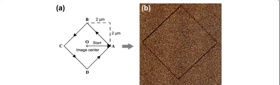
and an example for generating diamond was represented in the following. The diamond pattern was designed in Figure 3a; according to the matching program, the tip hammered the film surface after moving 2 μm from the center of the scan field to create a diamond with a diag-onal scale of 4μm. The matching C program was listed as the following:
#include < litho.h>
extern“C”__declspec(dllexport) int macroMain()
{
LITHO_BEGIN
LithoDisplayStatusBox(); // displays litho status box LithoScan(false); // turns off scanning
LithoCenterXY(); // moves tip to the center of the field // declares cyclic variable
int i = 1;
double size = 2.0; //declares translation distances of 2
μm fromOtoA
double rate = 1.0; // declares the rate of 1μm/s for
moving tip
double vSetPoint = 0.90; // declares a Setpoint of 0.9 for when hammering surface
LithoTranslate( size, 0, rate); // moves the tip to the
first corner (A)
LithoSet(lsSetpoint,vSetPoint); // sets the Setpoint value at 0.9
for(i = 1;i < =5;i++) // hammers the same patterns repeatedly for five times
normal scanning
[image:4.595.59.539.558.704.2]The command sentence of Lithoset(lsSetpoint,vSetPoint) was used to set the tapping load for the AFM tip, and the sentence double vSetPoint = 0.90 was used to modulate thesetpointvalue at 0.9 for hammering nano-patterns. As shown in Figure 3a, the LithoTranslate (size, 0, rate) com-mand was used to move the tip from centerOto pointA by a distance of 2 μm; the command of LithoTranslate (−size, size, rate) moved the tip from pointAtoBto ham-mer sideABof the diamond by declaring the parameters− size, size or movements in negativeXand positiveY, and the moving rate was 1.0μm/s by declaring the sentence of double rate = 1.0. The tip then proceeded to hammer the remaining sides of the diamond shape (sides BC, CD and DA) onto the sample surface. A loop program for (i = 1; i < =5;i++) was written into the program so that the tip continued to hammer the pattern route continuously for five times to improve surface indentation and resolution, creating much clearer patterns. After the AFM tip com-pleted all the sentences or commands in the above pro-gram, a perfect diamond pattern on the structure-tailored thin SEBS film was generated automatically, as shown in Figure 3b. Besides the simple patterns, more complicated imprinted or embossed high resolution nano-patterns can also be generated by using the automatic hammering method, simply by designing and changing the defined corresponding program that controls the tip movement route. Figure 4a-c shows a variety of more complicated
patterns; Figure 4a shows an imprinted five-pointed star, Figure 4b shows an embossed word HIT, and Figure 4c shows imprinted Chinese characters with minimum line-width of 18 nm. All the nano-patterns prove that auto-matic hammering method can be used to fabricate more complicated patterns with high resolution and speed.
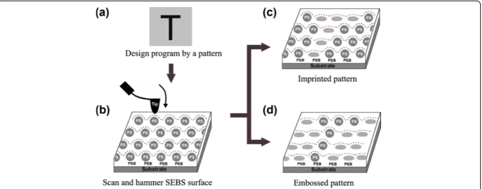
[image:5.595.56.539.90.210.2]A schematic process for the automatic hammering lithography is shown in Figure 5a-d. First and foremost, a computer program is of upmost importance for a per-fect outcome, so a corresponding program is designed for ‘writing’a pattern, i.e.,‘T’, represented in Figure 5a. The next step involves scanning over the SEBS film sur-face to confirm the suitability for AFM tip hammering, and the sample surface is scanned in light tapping mode to select a large area suitable for hammering. Shown in Figure 5b is the hexagonal-spherical PS microdomains embedded in the PEB matrix. The curved dash lines over PS spheres represent an AFM tip indented surface under
light tapping conditions (non-lithographed SEBS surface); Lastly, the sample surface was hammered by oscillating AFM tip with a predefined route and load by the program. The plastic PS microdomains can therefore be selectively hammered from spheres to ellipsoids, and the indentation contrast between the spherical and ellipsoidal PS microdo-mains gives rise to either imprinted T pattern (Figure 5c) or embossed T pattern (Figure 5d).
In the past studies of mechanical force nanolithography [15-17,22,23], tip plowing causes a significant reduction in the practical linewidth resolution, with cantilever torsion producing edge irregularities or sidewalls of piled up deb-ris on each side of a scratch line. The edge irregularities can be overcome on SEBS films with hexagonal-spherical microstructure by using ATHN manual procedures [19]; while the hammering process and overall operation are very difficult, being limited to hammering individual lines in any single step of the procedure. This costs much time,
[image:5.595.60.540.488.676.2]Figure 4AFM phase images of nano-patterns by automatic hammering technique.(a) imprinted 5-pointed star pattern; (b) embossed pattern-word HIT; (c) imprinted Chinese characters. Image size: 2.0 × 2.0μm2.
the corresponding design program can be hammered re-peatedly to duplicate the same patterns for many times, and the pattern size can also be changed easily through adjusting the program parameters. This new automatic hammering method overcomes some common drawbacks of previous AFM nanolithography methods [15-17,22,23], such as expertise operating skill, expensive diamond tips, tip wearing, and low efficiency. Most importantly, it is well known that the existence (or absence) of a spot of the local indentation can represent‘0’or‘1’of a digital mode in a data storage context. The preexisted dot array pattern and shape memory effect of this block copolymer media therefore offer particular applicability in the field of high density data storage should we are able to selectively in-dent dot-array patterns at predefined positions using this newly developed auto-hammering method, which will be reported later. The limitation of the present hammering nanolithography is that the writing media has to be the specially tailored block copolymer films.
Conclusions
A high-speed automatic nanolithography technique is pro-posed in this article, in which a vibrating AFM tip is used to generate both imprinted and embossed nano-patterns with 18 nm linewidth resolution on structure-tailored thin SEBS block copolymer film. In the process for generating the complex nano-patterns, the route path of the tip move-ment is precisely controlled in accordance to a predefined computer program. Results show that this technique allows any complex high resolution nano-patterns to be ham-mered on thin SEBS film of spherical microstructure using conventional AFM instrumentation in tapping mode, or-dinary silicon tip, and appropriately designed pattern pro-gram. In comparison with conventional mechanical force nanolithography, this automatic nanolithography technique has some advantages, such as having no edge irregularities or sidewalls around the imprint pattern and having high resolution and high efficiency. Therefore, the auto-hammering method will become a promising lithography technique in the near future and has the potential for appli-cation in the fields of data storages, microelectronics, nano-technology, and miniature sensors.
Competing interests
The authors declare that they have no competing interests.
Shuter for manuscript check and revision.
Author details
1College of Materials Science and Engineering, Liaoning Technical University,
Fuxin 123000, China.2Materials Physics and Chemistry Department, Harbin Institute of Technology, Harbin 150001, China.3Key Laboratory of
Micro-Systems and Micro-Structures Manufacturing, Ministry of Education, Harbin 150001, China.
Received: 17 May 2012 Accepted: 22 July 2012 Published: 13 August 2012
References
1. Jin X, Unertl WN:Submicrometer modification of polymer surfaces with a surface force microscope.Appl Phys Lett1992,61:657.
2. Xu QB, Stewart M, Ryan D, Willson CG, Whitesides GM:New approaches to nanofabrication: molding, printing, and other techniques.Chem Rev2005,
105:1171.
3. Garcia R, Perez R:Dynamic atomic force microscopy methods.Surf Sci Rep 2002,47:197.
4. Garcia R, Magerle R, Perez R:Nanoscale compositional mapping with gentle forces.Nat Mater2007,6:405.
5. Garcia R, Martinez RV, Martinez J:Nano-chemistry and scanning probe nanolithographies.Chem Soc Rev2006,35:29.
6. Garcia R, Calleja M, Perez-Murano F:Local oxidation of silicon surfaces by dynamic force microscopy: nanofabrication and water bridge formation. Appl Phys Lett1998,72:2295.
7. Perez-Murano F, Abadal G, Barniol N, Aymerich X, Servat J, Gorostiza P, Sanz F:Nanometer-scale oxidation of Si(100) surfaces by tapping mode atomic force microscopy.J Appl Phys1995,78:6797.
8. Gan YJ, Wong HY, Lee WP:A novel atomic force microscopy based lithography system for automated patterning via anodic oxidation.
Compos Part B: Eng2011,42:456.
9. Tseng AA:Removing material using atomic force microscopy with single- and multiple-tip sources.Small2011,7:3409.
10. Vettiger P, Despont M, Drechsler U, Durig U, Haberle W, Lutwyche MI, Rothuizen HE, Stutz R, Widmer R, Binnig GK:The“Millipede”-more than thousand tips for future AFM data storage.IBM J Res Dev2000,44:323. 11. Pires D, Hedrick JL, De Silva A, Frommer J, Gotsmann B, Wolf H, Despont M,
Duerig U, Knoll AW:Nanoscale three-dimensional patterning of molecular resists by scanning probes.Science2010,328:732.
12. Jegadesan S, Sindhu S, Valiyaveettil S:Easy writing of nanopatterns on a polymer film using electrostatic nanolithography.Small2006,2:481. 13. Kunze U, Klehn B:Plowing on the sub-50 nm scale: nanolithography
using scanning force microscopy.Adv Mater1999,11:1473. 14. Sohn LL, Willett RL:Fabrication of nanostructures using
atomic-force-microscope-based lithography.Appl Phys Lett1995,67:1552. 15. Heyde M, Rademann K, Cappella B, Geuss M, Sturm H, Spangenberg T,
Niehus H:Dynamic plowing nanolithography on polymethylmethacrylate using an atomic force microscope.Rev Sci Instrum2001,72:136. 16. Cappella B, Sturm H:Breaking polymer chains by dynamic plowing
lithography.Polymer2002,43:4461.
17. Cappella B, Sturm H:Comparison between dynamic plowing lithography and nanoindentation methods.J Appl Phys2002,91:506.
18. Wang Y, Hong XD, Liu BQ, Ma CY, Zhang CF:Two-dimensional ordering in block copolymer monolayer thin films upon selective solvent annealing.
Macromolecules2008,41:5799.
20. Hong XD, Gan Y, Wang Y:Facile measurement of polymer film thickness ranging from nanometer to micrometer scale using atomic force microscopy.Surf Interface Anal2011,43:1299.
21. NanoLithography Software Version 5.12:Digital Instruments Veeco Metrology Group 2001. http://www.google.com.hk/url?sa=t&rct=j&q=NanoLithography +Software+Version+5.12.
22. Tseng AA, Shirakashi J, Jou S, Huang JC, Chen TP:Scratch properties of nickel thin films using atomic force microscopy.J Vac Sci Technol B2010,
28:202.
23. Irmer B, Blick RH, Simmel F, Godel W, Lorenz H, Kotthaus JP:Josephson junctions defined by a nanoplough.Appl Phys Lett2051,1998:73.
doi:10.1186/1556-276X-7-456
Cite this article as:Honget al.:Automatic hammering of nano-patterns on special polymer film by using a vibrating AFM tip.Nanoscale Research Letters20127:456.
Submit your manuscript to a
journal and benefi t from:
7 Convenient online submission 7 Rigorous peer review
7 Immediate publication on acceptance 7 Open access: articles freely available online 7 High visibility within the fi eld
7 Retaining the copyright to your article