N A N O E X P R E S S
Open Access
Strained GaAs/InGaAs Core-Shell Nanowires
for Photovoltaic Applications
K. Moratis
1, S. L. Tan
2,3, S. Germanis
1,4, C. Katsidis
1, M. Androulidaki
4, K. Tsagaraki
4, Z. Hatzopoulos
4,5, F. Donatini
3,6,
J. Cibert
3,6, Y. -M. Niquet
2, H. Mariette
3,6and N. T. Pelekanos
1,2,3,4*Abstract
We report on the successful growth of strained core-shell GaAs/InGaAs nanowires on Si (111) substrates by molecular beam epitaxy. The as-grown nanowires have a density in the order of 108cm−2, length between 3 and 3.5μm, and diameter between 60 and 160 nm, depending on the shell growth duration. By applying a range of characterization techniques, we conclude that the In incorporation in the nanowires is on average significantly smaller than what is nominally expected based on two-dimensional growth calibrations and exhibits a gradient along the nanowire axis. On the other hand, the observation of sharp dot-like emission features in the micro-photoluminescence spectra of single nanowires in the 900–1000-nm spectral range highlights the co-existence of In-rich enclosures with In content locally exceeding 30 %.
Keywords:Core-shell GaAs/InGaAs nanowires, Nanostructure characterization, Micro-Raman, Photoluminescence, Cathodoluminescence, Micro-photoluminescence
Background
Semiconductor nanowires (NWs) and NW-based het-erostructures are currently under extensive research, due to the unique properties and prominent quantum phe-nomena emerging from them. For instance, there are numerous reports of NW structures containing quantum dots, which can act as efficient sources of single photons or entangled photon pairs [1–5]. Another application area where NW arrays attract wide interest is in next-generation cost-effective and high-efficiency photovoltaic (PV) devices, based on two main reasons: first, their re-laxed lattice-matching requirements, due to easy strain accommodation at the NW free surface, providing flexi-bility in substrate selection and band-gap engineering. Second, the possibility for lesser material utilization, due to enhanced light absorption in NW arrays, based on their inherent anti-reflecting properties [6], increased light trapping within the array [7], and resonant wave-guiding properties [8]. Recently, a single-junction solar cell based on InP NWs [9] with an efficiencyη≈13.8 %
and a single GaAs NW PV device [10] with η≈40 % have been reported, showing the real potential of NW solar cells to compete directly with other thin-film solar cell technologies. Another direction worth exploring for NW solar cells is the possibility to utilize piezoelectric (PZ) fields present in strained NW heterostructures, in order to obtain enhanced NW-based PV devices. As first estimated by Boxberg et al. [11], a significant axial PZ field of 60–80 kV/cm can develop in InAs/InP core-shell NWs, which can be used for efficient carrier sweeping towards the device electrodes. As we have recently shown in [12], axial PZ fields of the order of 7–8 kV/cm may even exist in core-shell GaAs/AlGaAs NWs, having a very small lattice mismatch of 0.05 %. Such fields are already significant for the operation of a PV device and should be taken into account in any related device work. In this work, we report on the preliminary results of the growth and characterization of strained core-shell GaAs/ InGaAs NWs, a NW heterostructure which is expected to exhibit pronounced PZ effects.
Methods
GaAs/InGaAs core-shell NWs are grown in a VG Semicon V80H III-As solid-source molecular beam epi-taxy (MBE) system via the vapor liquid solid (VLS) * Correspondence:pelekano@materials.uoc.gr
1Department of Materials Science and Technology, University of Crete, P.O.
Box 2208, 70013 Heraklion, Greece
2CEA, INAC, 17 rue des Martyrs, 38054 Grenoble cedex 9, France
Full list of author information is available at the end of the article
mechanism on n+ Si (111) substrates (manufactured by Siltronix). The native oxide-capped Si substrate is loaded into the MBE growth chamber without prior chemical treatment and is annealed in situ at 650 °C for 10 min in order to create pinholes in the native oxide layer that act as nucleation sites for GaAs NWs. The core-shell config-uration is achieved by first growing GaAs NWs (“core”) and then encapsulating the GaAs core by a two-dimensional (2D) epitaxial growth of InGaAs shell. A substrate temperature of 600 °C is used for the growth of the GaAs core NWs. Ga droplets are deposited in situ at a flux of 0.4 ML/s for 20 s to act as catalysts that initi-ate the VLS growth of the GaAs core NWs. Note that the Ga and As fluxes are quoted in terms of the equiva-lent 2D growth rates estimated from RHEED oscillation analysis during Ga- and As-limited GaAs growths on GaAs (100) surfaces. Following Ga droplet deposition, the shutter of the Ga Knudsen cell (K-cell) is closed for 20 s to allow Ga to relax on the substrate surface and form droplets of uniform diameter. The growth of the GaAs NWs is performed for 30 min using a Ga flux of 0.4 ML/s and an As/Ga flux ratio of ~2. These growth parameters result in GaAs core NWs with a diameter of ~60 nm, height of ~3μm, and density of 2 × 108cm−2. Following the growth of the GaAs core NWs, the InGaAs shell growth is initiated by exposing the sample to As flux for 10 min to remove the Ga droplets, while the As K-cell temperature is raised to increase the As/ Ga flux ratio to ~5. The substrate temperature is de-creased to 500 °C, which is optimal for 2D InGaAs growth. The InGaAs shell growth duration and In flux are varied for each sample in order to achieve NWs with different shell thicknesses and In to Ga stoichiometry. In total, three sets of samples have been grown in different days. Each set comprises three GaAs/InGaAs core-shell NW samples and one GaAs core NW reference sample. In the first set of samples, the InGaAs shell growth dur-ation is fixed at 40 min, while the In flux is varied to produce nominal In shell contents of 2, 5, and 9.5 %, based on 2D InGaAs thin-film calibrations. In the sec-ond and third sets of samples, the In flux is fixed with a beam equivalent pressure of 4.55 × 10⁻⁸ mbar, corre-sponding to a nominal In content of 9.5 %, while the InGaAs shell growth duration is varied, as summarized in Table 1. Finally, the InGaAs shell is passivated (from
oxidation when exposed to the air) by a 3-min growth of a thin GaAs cap layer, having an estimated thickness of about 3 nm.
The surface morphology and the structural character-istics of the NWs are investigated by performing field emission-scanning electron microscopy (FE-SEM) on the as-grown samples. The optical properties of the samples are studied by performing macro-PL measurements using a 325-nm He-Cd Kimmon laser. The macro-PL experimental setup consists of a closed circuit liquid He-cooled cryostat in which the sample is mounted and excited by a laser beam focused using a 10-cm quartz lens. The excitation power used for PL is limited to 0.23 mW because of photo-bleaching effects due to the activation of surface-related non-radiative channels [13], which are especially pronounced in the GaAs core NW reference samples. The PL signal is analyzed by a 0.5-m spectrograph with a 600 gr/mm grating and is recorded by a liquid nitrogen (LN)-cooled charge-coupled device (CCD) camera.
In addition, micro-Raman, cathodoluminescence (CL) and micro-PL measurements have been performed on individual GaAs/InGaAs core-shell NWs dispersed on Si substrate with gold metal grid to assist with the identifi-cation and tracking of individual NWs of interest. A Nicolet Almega XR micro-Raman setup is used for the micro-Raman measurements, which consists of a 473-nm diode laser with the beam focused to a spot size of 0.5μm using a ×100 microscope objective with 1.25 nu-merical aperture (NA). The Raman spectra are analyzed by a 2400-gr/mm grating and are recorded by a CCD camera. For the micro-PL measurements, the sample (with NWs dispersed on grid) is mounted on a LN flow cryostat and excited using the 750-nmcwline of a tunable Ti:Sapphire laser, with the beam focused to a spot size of ~1 μm using a ×40 microscope objective with 0.65 NA. The micro-PL signal is analyzed by a 0.75-m spectrograph utilizing a 600-gr/mm grating and is re-corded by a back-thinned LN-cooled CCD camera with high quantum efficiency. CL measurements at 5 K are car-ried out in a FEI Inspect F50 FE-SEM system, which is equipped with a Gatan cryogenic stage and a custom in-house-made light collection system. The CL mappings are recorded over a ±3-nm spectral window using a Horiba IHR 550 spectrometer equipped with a photomultiplier.
Results and Discussion
[image:2.595.57.291.667.732.2]As a further motivation for studying the GaAs/InGaAs NW heterostructure in view of PV applications, we plot in Fig. 1 the calculated PZ potential profile over a cross section of a core-shell NW with a 70-nm-wide GaAs core and a 40-nm-thick In0.05Ga0.95As shell. In this cal-culation, the structure is relaxed with Keating’s valence force field [14]. Then, the PZ polarization density is
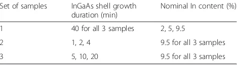
Table 1InGaAs shell growth duration and nominal In content of the samples grown for this study
Set of samples InGaAs shell growth duration (min)
Nominal In content (%)
1 40 for all 3 samples 2, 5, 9.5
2 1, 2, 4 9.5 for all 3 samples
computed from the strain tensor εijand Poisson’s equa-tion is solved for the PZ potential. A virtual alloy is as-sumed in the InGaAs shell (averaging the elastic and piezoelectric constants of InAs and GaAs). Details can be found in [14]. Aside from the axial component of the PZ polarization which can generate significant axial PZ fields, as mentioned above, we show in Fig. 1 that the lateral components of the PZ polarization give rise to the formation of periodic maxima and minima in the potential profile with a clear triangular symmetry. The potential difference between the maxima and minima is already ~100 mV in the given heterostructure, which is substantial enough to ensure that the photo-generated charge carriers will be efficiently separated in different parts of the NW, thus minimizing the carrier recombin-ation losses—a very important parameter in optimizing PV devices.
Typical FE-SEM images of core-shell GaAs/InGaAs NWs are shown in Fig. 2, where we observe that over 60 % of the NWs are grown along the [111] direction
perpendicular to the substrate, while the rest grow along inclined {111} crystallographic orientations, consistent with results reported previously for similar growth con-ditions [15, 16]. By closer inspection of the SEM images, most of the core-shell NWs display characteristic hex-agonal morphology with {110} lateral facets (cf. inset of Fig. 2a), as well as a small tapering effect with the NW diameter increasing by 5–10 % along the NW growth axis (cf. Fig. 2c). Among the SEM images of the three GaAs core NW reference samples, no significant vari-ation in the NW density and dimensions is observed from sample to sample, signifying a good control of the VLS growth conditions. The average diameter of the GaAs core NWs is 58 nm, the average length is 3 μm, and the density is in the order of 108nanowires per cm2. In the case of GaAs/InGaAs core-shell NWs, an InGaAs shell growth duration between 1 and 40 min results in average InGaAs shell thickness between 1 and 50 nm. On the other hand, the average NW length only in-creases gradually from 3 to 3.5 μm for InGaAs shell growth duration between 0 (i.e., without shell) and 40 min. This suggests that the growth rates at the NW tips are 5–10 times higher than at the lateral facets. Consequently, an InGaAs region forms around the tip, with a length about 5–10 times the InGaAs shell thick-ness. The higher growth rates at the NW tip can be attributed to “shadowing” effect and to varying growth rates at the different crystallographic planes of the tip and lateral facets.
Next, we attempt to characterize the actual incorpor-ation and distribution of In in the core-shell NWs. Energy-dispersive X-ray (EDX) analysis on a range of relatively large areas (1–105μm2) of the as-grown sam-ples reveal In contents that are in good agreement with the nominal values. For instance, EDX gives an In con-tent of 7.5 % for the sample of Fig. 2, compared with the 9.5 % nominal concentration. However, due to the rela-tively low NW density, most of the In signal in such EDX scans originates from the polycrystalline InGaAs
Fig. 1Piezoelectric potential profile for an electron in a cross section of a core-shell nanowire with 70-nm-wide GaAs core and 40-nm-thick In0.05Ga0.95As shell
[image:3.595.56.291.87.259.2] [image:3.595.60.541.577.702.2]2D layer formed at the interface with the Si substrate in between the NWs. In other words, the EDX results may not necessarily represent the true level of In incorpor-ation in the InGaAs NW shell. EDX measurements on single NWs were not conclusive because the In signal was below the detection limit of the system.
To further investigate the question of In incorporation and distribution in the NWs, micro-Raman measure-ments were performed on single NWs dispersed on a grid (Fig. 3). In Fig. 3a, typical micro-Raman spectra from a single GaAs/InGaAs core-shell NW are depicted and compared with a GaAs (111)B substrate. The NW spectra are obtained from three different points along the NW axis, as indicated in the optical microscope im-ages of Fig. 3b. Considering the small tapering of the NW, better distinguished in the SEM image of Fig. 3c, point 1 corresponds to the bottom part of the NW, and point 3 to the top part of the NW (“tip”). The In content can be estimated by comparing the positions of the pho-non peaks with the relations found in the literature [17] for the GaAs-like longitudinal optical (LO) and trans-verse optical (TO) phonon modes of InxGa1−xAs. In Fig. 3a, both phonon modes seem to shift to lower wave numbers as the NW is scanned from the bottom to the top, suggesting that the In incorporation increases along the growth axis towards the NW tip. For the particular NW in Fig. 3, the In contents deduced from the LO phonon peaks are 1.7, 1.7, and 3 % for pointsp1,p2, and p3, respectively, while the corresponding values from the TO phonon peaks are 2.7, 4.7, and 6.7 %, respectively. This highlights the fact that the In contents determined by the Raman shifts of the LO phonons are systema-tically lower than the values obtained from the TO pho-nons. We interpret this as an effect of strain in the InGaAs shells affecting the TO and LO phonons in op-posite directions [18]. To take into account this strain effect, we employ the average value of the In contents,
determined by the two phonon modes. Hence, the aver-age In content for the specific NW of Fig. 3 would be 2.2 % at the bottom, 3.2 % in the middle, and 4.8 % to-wards the top. Similar findings have been found in at least another 15 NWs studied, allowing us to conclude that the In incorporation in the core-shell structure ex-hibits gradients along the NW axis and is on average sig-nificantly smaller than what is nominally expected, which can be attributed to different In incorporation in the various crystallographic planes of the NW structure.
The above finding of smaller In incorporation in the NWs appears to agree with the emission properties of the as-grown samples. In Fig. 4a, we show a typical low-temperature PL spectrum from a core-shell NW sample with ≈50-nm shell thickness. Focusing first on the high energy side, we distinguish two GaAs core-related peaks at 1.509 and 1.500 eV, which are assigned as emission from GaAs-free-like excitons (FX) and excitons bound to neutral acceptors (A0X), respectively [19]. This assign-ment is justified by their temperature dependence, as shown in Fig. 4b, where we observe a rapid ionization of the A0X peak with temperature, while the FX line per-sists and dominates the whole spectrum. In Fig. 4c, we compare the FX emission peaks of the core-shell NWs with ≈50-nm shell thickness, an undoped GaAs bulk sample, and the reference GaAs NWs. A first observa-tion is that the FX peak of the reference GaAs NWs, sit-uated at 1.520 eV, is blueshifted by as much as 4.5 meV with respect to the FX position of bulk GaAs. This blue-shift is attributed to quantum confinement effects as the NW diameter decreases [20]. On the other hand, the FX peak of the core-shell NW sample is characteristically redshifted with respect to the reference GaAs NWs, and as shown in Fig. 4d, the redshift increases with the InGaAs shell thickness, clearly suggesting that it is caused by the strain imposed to the core by the shell layer. Similar redshifts have been observed previously in
[image:4.595.60.539.555.692.2]other systems including GaAs/AlGaAs NWs [12]. It can be shown [21] that the strain-induced variation of the gap in the core layer can be written as
EX ¼E0X−ðacþaυÞ⋅
c11−c12þ6c44
c11þc12þ2c44⋅f
1−η
ð Þ
− dffiffiffi 3
p ⋅ c11þ2c12
c11þc12þ2c44⋅f
1−η
ð Þ
where, aside from the elastic constants and deformation potentials of the core material, fis the lattice mismatch between GaAs and InGaAs and (1−η) is the cross-sectional area ratio between the InGaAs shell and the full core-shell structure, including the GaAs cap layer. The dependence on the shell thickness is contained in this area ratio. Using GaAs parameters [22], the average
core and core-shell NW diameters and a 3-nm GaAs cap layer thickness, we can reproduce the data as repre-sented by the solid line in Fig. 4d, assuming a lattice mismatch of ~0.1 %. This value corresponds to an aver-age In concentration in the shell layer of merely ~1.5 %, in good agreement with the micro-Raman results.
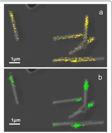
[image:5.595.57.541.88.475.2]Returning to the full PL spectrum of the core-shell NWs in Fig. 4a, the InGaAs shell gives rise to a broad emission spectrum from about 1.48 eV down to 1.23 eV. The intense PL peak around 1.46–1.47 eV, which is present in all core-shell NW samples with shell thick-nesses above 10 nm, cannot be attributed to donor-acceptor-type recombination [23] in the GaAs core for two reasons: firstly, because it dramatically acquires strength as the shell thickness increases, as visible in Fig. 4e, and secondly, based on the CL measurements
[image:5.595.71.251.590.642.2]that will be discussed next. In Fig. 5, typical CL mappings spectrally filtered at two different energies are shown from an ensemble of dispersed core-shell NWs on a grid. While the GaAs core emission at 1.508 ± 0.005 eV (top) seems to originate from nearly the whole length of the NW, the emission at 1.475 ± 0.005 eV (bottom) is localized on one end of the NW which, based on the slight tapering effect, corresponds systematically to the NW tip. As explained above, the NW tip consists of an InGaAs region of several hundreds of nanometers in length, without the GaAs core; based on its emission energy [24] and neglecting any confinement effect, the In content at the NW tip can be estimated around 4 %, again in good agreement with the micro-Raman results.
To understand the nature of the InGaAs-related emis-sion at energies below 1.4 eV, micro-PL measurements are performed on single NWs. Typical micro-PL spectra at 80 K as a function of power are shown in Fig. 6, where at low powers “sharp” dot-like emission features are observed at energies as low as 1.25 eV, strongly sug-gesting the existence of In-rich enclosures. From the en-ergy position, we can estimate that the local In content should be larger than 30 %. With increasing excitation power, a spectacular power-dependent evolution of the
spectra is observed, with the emission spectra blueshift-ing due to successive state fillblueshift-ing effects. The micro-PL signature differs not only from one NW to another but also between different parts of the same NW, suggesting the formation of In-rich enclosures in various parts of the NW. At this stage, it is not possible to distinguish whether the In-rich enclosures are in the form of chan-nels along the <112> direction [25, 26], or in the form of In shell aggregates in a quantum dot-like structure [27]. Ongoing high-resolution TEM measurements and time-resolved micro-PL will shed more light on the structural properties of the InGaAs shell and the morphology of the presumed In-rich enclosures mentioned above.
Conclusions
Strained core-shell GaAs/InxGa1−xAs nanowires with nominal In content between 2 and 9.5 % have been suc-cessfully grown on Si (111) substrates, with the majority of the nanowires growing vertical to the substrate. The as-grown nanowires are 3–3.5 μm long, have a density of about 108 cm−2, a core diameter of ~60 nm, and an InGaAs shell thickness ranging from 1 to 50 nm, depending on the shell growth duration. By applying a range of optical and structural characterization tech-niques, we conclude that the In incorporation in the nanowires is on average significantly smaller than the nominal In content estimated from 2D InGaAs growth calibrations. The In content also exhibits a gradient along the nanowire axis, with higher In content at the tip compared with the lateral facets, which can possibly be attributed to different In incorporation rates in the various crystallographic planes of the nanowire surface. Moreover, the dot-like emission spectra of single nano-wires show evidence of the formation of In-rich enclo-sures with an In content higher than 30 %.
Fig. 5(color online) Typical CL mappings at T = 5 K from a bundle of dispersed nanowires on Si, spectrally filtered at the indicated energies of (a) 1.508 ± 0.005 eV (top), where a relatively uniform emission attributed to the GaAs core is observed along the nanowire, and (b) 1.475 ± 0.005 eV (bottom) where strong emission from InGaAs is obtained at the nanowire tip. Thescale baris 1μm
[image:6.595.306.539.88.263.2] [image:6.595.58.291.388.665.2]Competing Interests
The authors declare that they have no competing interests.
Authors’Contributions
KM carried out the PL experiments, performed most of the analysis of experimental results, and drafted a first manuscript. SLT and ZH carried out the MBE experiments. SG performed the micro-PL; MA micro-Raman; FD cathodoluminescence, and KT, SEM, and EDX experiments. CK and YMN carried out the simulations. JC and HM made substantial contributions in the interpretation of data and revised critically the manuscript. NTP led the effort and produced the final manuscript. All authors read and approved the final manuscript.
Acknowledgements
This work is funded by the Chair of Excellence program of the“Laboratoire d’excellence LANEF in Grenoble (ANR-10-LABX-51-01)”and the European Social Fund and National resources through the THALES program “NANOPHOS,”the ARISTEIA II program“NILES,”and the PROENYL research project, Action KRIPIS, project MIS-448305.
Author details
1
Department of Materials Science and Technology, University of Crete, P.O. Box 2208, 70013 Heraklion, Greece.2CEA, INAC, 17 rue des Martyrs, 38054
Grenoble cedex 9, France.3UniversitéGrenoble Alpes, F-38000 Grenoble,
France.4Microelectronics Research Group, IESL-FORTH, P.O. Box 1385, 71110
Heraklion, Greece.5Department of Physics, University of Crete, P.O. Box 2208, 70013 Heraklion, Greece.6CNRS, Institut NEEL, F-38000 Grenoble, France.
Received: 10 December 2015 Accepted: 21 March 2016
References
1. Borgström MT, Zwiller V, Müller E, Imamoglu A (2005) Optically bright quantum dots in single nanowires. Nano Lett 5:1439–43. doi:10.1021/nl050802y 2. Holmes MJ, Choi K, Kako S et al (2014) Room-temperature triggered single
photon emission from a III-nitride site-controlled nanowire quantum dot. Nano Lett 14:982–986. doi:10.1021/nl404400d
3. Kats VN, Kochereshko VP, Platonov AV et al (2012) Optical study of GaAs quantum dots embedded into AlGaAs nanowires. Semicond Sci Technol 27:015009. doi:10.1088/0268-1242/27/1/015009
4. Kwoen J, Watanabe K, Ota Y et al (2013) Growth of high-quality InAs quantum dots embedded in GaAs nanowire structures on Si substrates. Phys status solidi 10:1496–1499. doi:10.1002/pssc.201300316
5. Singh R, Bester G (2009) Nanowire quantum dots as an ideal source of entangled photon pairs. Phys Rev Lett 103:1–4. doi:10.1103/PhysRevLett.103.063601 6. Hu L, Chen G (2007) Analysis of optical absorption in silicon nanowire arrays
for photovoltaic applications. Nano Lett 7:3249–52. doi:10.1021/nl071018b 7. Tsakalakos L, Balch J, Fronheiser J et al (2007) Strong broadband optical
absorption in silicon nanowire films. J Nanophotonics 1:013552. doi:10.1117/1.2768999
8. Lin C, Povinelli ML (2009) Optical absorption enhancement in silicon nanowire arrays with a large lattice constant for photovoltaic applications. Opt Express 17:19371–81. doi:10.1364/OE.17.019371
9. Wallentin J, Anttu N, Asoli D et al (2013) InP nanowire array solar cells achieving 13.8% efficiency by exceeding the ray optics limit. Science 339(80-):1057–1060. doi:10.1126/science.1230969
10. Krogstrup P, Jørgensen HI, Heiss M et al (2013) Single-nanowire solar cells beyond the Shockley-Queisser limit. Nat Photonics 7:306. doi:10.1038/NPHOTON.2013.32
11. Boxberg F, Søndergaard N, Xu HQ (2010) Photovoltaics with piezoelectric core-shell nanowires. Nano Lett 10:1108–12. doi:10.1021/nl9040934 12. Hocevar M, Thanh Giang LT, Songmuang R et al (2013) Residual strain and
piezoelectric effects in passivated GaAs/AlGaAs core-shell nanowires. Appl Phys Lett 102:191103. doi:10.1063/1.4803685
13. Shi X, Tu Y, Liu X et al (2013) Photobleaching of quantum dots by non-resonant light. Phys Chem Chem Phys 15:3130–2. doi:10.1039/c3cp43668c 14. Niquet Y (2006) Electronic and optical properties of InAs∕GaAs nanowire
superlattices. Phys Rev B 74:155304. doi:10.1103/PhysRevB.74.155304 15. Giang LTT, Bougerol C, Mariette H, Songmuang R (2013) Intrinsic limits
governing MBE growth of Ga-assisted GaAs nanowires on Si(111). J Cryst Growth 364:118–122. doi:10.1016/j.jcrysgro.2012.11.032
16. Kehagias T, Florini N, Kioseoglou J et al (2015) Nanostructure and strain properties of core-shell GaAs/AlGaAs nanowires. Semicond Sci Technol 30:114012. doi:10.1088/0268-1242/30/11/114012
17. Islam MR, Verma P, Yamada M et al (2002) Micro-Raman characterization of starting material for traveling liquidus zone growth method. Japanese J Appl Physics, Part 1 Regul Pap Short Notes Rev Pap 41:991–995. doi:10.1143/JJAP.41.991
18. Stergiou VC, Pelekanos NT, Raptis YS (2003) Piezoelectric effect on the optical phonon modes of strained cubic semiconductors: case of CdTe quantum wells. Phys Rev B - Condens Matter Mater Phys 67:1653041–16530415. doi:10.1103/PhysRevB.67.165304
19. Pavesi L, Guzzi M, Fisica D, et al. Photoluminescence of AlxGa1xAs alloys photoluminescence. J Appl Phys. 2011. doi: 10.1063/1.355769
20. Zhang G, Tateno K, Sanada H et al (2009) Synthesis of GaAs nanowires with very small diameters and their optical properties with the radial quantum-confinement effect. Appl Phys Lett 95:4–7. doi:10.1063/1.3229886 21. Ferrand D, Cibert J (2014) Strain in crystalline core-shell nanowires. Eur Phys
J Appl Phys 67:30403. doi:10.1051/epjap/2014140156
22. Vurgaftman I, Meyer JR, Ram-Mohan LR (2001) Band parameters for III–V compound semiconductors and their alloys. J Appl Phys 89:5815. doi:10.1063/1.1368156
23. Bogardus EH, Bebb HB (1968) Bound-exciton, free-exciton, band-acceptor, donor-acceptor, and Auger recombination in GaAs. Phys Rev 176:993–1002. doi:10.1103/PhysRev.176.993
24. O’Donnell KP, Chen X (1991) Temperature dependence of semiconductor band gaps. Appl Phys Lett 58:2924–2926. doi:10.1063/1.104723 25. Rudolph D, Funk S, Döblinger M et al (2013) Spontaneous alloy composition
ordering in GaAs-AlGaAs core-shell nanowires. Nano Lett 13:1522–1527. doi:10.1021/nl3046816
26. Heiss M, Fontana Y, Gustafsson A et al (2013) Self-assembled quantum dots in a nanowire system for quantum photonics. Nat Mater 12:439–44. doi:10.1038/nmat3557
27. Uccelli E, Arbiol J, Morante JR, Morral AFI (2010) InAs quantum dot arrays decorating the facets of GaAs nanowires. ACS Nano 4:5985–5993. doi:10.1021/nn101604k
Submit your manuscript to a
journal and benefi t from:
7 Convenient online submission
7Rigorous peer review
7 Immediate publication on acceptance
7Open access: articles freely available online
7 High visibility within the fi eld
7Retaining the copyright to your article