N A N O E X P R E S S
Open Access
Thickness dependency of field emission in
amorphous and nanostructured carbon thin films
Maziar Shakerzadeh
1, Edwin Hang Tong Teo
2and Beng Kang Tay
1,3*Abstract
Thickness dependency of the field emission of amorphous and nanostructured carbon thin films has been studied. It is found that in amorphous and carbon films with nanometer-sizedsp2clusters, the emission does not depend on the film thickness. This further proves that the emission happens from the surfacesp2sites due to large enhancement of electric field on these sites. However, in the case of carbon films with nanocrystals of preferred orientation, the emission strongly depends on the film thickness.sp2-bonded nanocrystals have higher aspect ratio in thicker films which in turn results in higher field enhancement and hence easier electron emission.
Keywords:Carbon films, Preferred orientation, Field emission
Background
Field emission (FE) from amorphous and nanostructured carbon thin films is widely studied in the past few years [1-7]. Understanding the emission mechanism and redu-cing the threshold field at which the emission occurs (Fth) are the main two subjects of interest. Amorphous
carbon (a-C) films are formed from carbon atoms ofsp2 andsp3hybridization [8]. Mechanical and physical prop-erties of a-C films strongly depend on thesp2percentage as well as the presence and size ofsp2(sub) nanoclusters embedded insp3matrix.
Different field enhancement mechanisms have been proposed for easy electron emission from carbon thin films. Robertson found that for different types of carbon films (hydrogenated, nitrogenated, etc.), there is an optimumsp2cluster size at which the emission occurs at the lowest possible Fth [8]. Based on this observation,
Carey et al. [2] have proposed that the large field en-hancement of carbon films is mainly due to the presence and distribution of conductive sp2nanoclusters embed-ded in insulative sp3matrix. The presence of a conduct-ive sphere embedded in an insulating matrix leads to small field enhancement. However, the presence of two
or more such spheres can further increase the
enhancement; for instance, the field enhancement of two conductive spheres in the bispherical coordination sys-tem was studied, and it was found that the presence of two gold spheres which are placed 5 nm apart from each other results in enhancements of 56 which can be increased to 400 for a 1-nm separation [9]. Based on this theory, the emission only occurs from the surface clus-ters and hence is independent of the thickness.
Despite the above-mentioned theory, Forrest et al. [3] studied the effect of different parameters including film thickness on FE of pure, nitrogenated, and hydrogenated a-C thin films. They found an optimum thickness for the lowest Fthin hydrogenated and nitrogenated carbon
films. Since there is no correlation between the surface microstructure and the film thickness, this finding is obviously in contradiction with the mechanism proposed by Carey et al. [2]. The only mechanism which can be used to describe the thickness dependency of FE is space-charge interlayer-induced band bending for semi-conductors [10]. Carrier depletion across the film thick-ness results in field enhancement at the Si/C interface; therefore, the electrons will be emitted from the conduc-tion band of the silicon substrate to highly curved conduction band of the film. At very thin samples, although emitted electrons possess very high energies, they still cannot overcome the emission barrier (the work function of the film). At very thick films, on the other hand, the electrons will lose energy while they are passing the film, and hence they cannot overcome the * Correspondence:ebktay@ntu.edu.sg
1
School of Electrical and Electronic Engineering, Nanyang Technological University, 50 Nanyang Avenue, Singapore 639798, Singapore
3
CINTRA, CNRS/NTU/THALES, UMI 3288, Research Techno Plaza, 50 Nanyang Drive, Border X Block, Level 6, Singapore 637553, Singapore
Full list of author information is available at the end of the article
emission barrier. Therefore, there is an optimum film thickness at which the emission occurs at the lowest possible field.
In another study, Zhao et al. [11] studied the thickness dependency of FE of a-C films. It was found that for a pure a-C film deposited at 200-V substrate bias, theFth
does not strongly depend on the film thickness. By chal-lenging the space-charge interlayer-induced band bend-ing model proposed by Forrest, they suggest that the F-N tunneling theory is the most suitable model to de-scribe the emission from a-C films.
More recently, the formation of preferred orientation [12-15] and the effect of this texture on properties of carbon films [16-18] attract lots of theoretical and ex-perimental attentions. In our previous work, we have shown that the formation of preferred orientation in the microstructure of the film results in an abrupt decrease in the Fth. It was discussed that the formation of
con-ductive sp2 channels throughout the thickness of the film results in the formation of high-aspect-ratio fila-ments which enhances the local field significantly.
In this paper, in order to reconfirm the mechanisms mentioned above, the thickness dependency of FE in amorphous (with different bonding structures) carbon films withsp2-bonded (sub) nanocrystals has been stud-ied. Besides, the thickness dependency of carbon films with nanocrystals of preferred orientation has been studied.
Methods
Filtered cathodic vacuum arc [19] was used to prepare different types of amorphous and nanocrystalline carbon films. Bonding structure of the films was controlled through controlling the negative substrate bias during the deposition. In order to fabricate carbon thin films with nanocrystals of preferred orientation, a carbon film deposited at 300-V substrate bias was irradiated by a sin-gle pulse of a 248-nm excimer laser with a pulse width of 23 ns. The laser energy was kept at 460 mJ/cm2. FE was tested in a parallel plate configuration with an in-dium tin oxide-coated glass as the cathode with an anode-cathode spacing of 100 μm in a pressure lower than 5 × 10⁻⁶Torr. In order to check the repeatability of the data, two samples were prepared at each condition. FE tests have been done on two different positions of every individual sample. More than ten measurements have been done on each test spot.
Results and discussion
Figure 1 shows the Raman spectra and thickness de-pendency of field emission from three different a-C films. The first film (Figure 1A,B) is a tetrahedral amorphous carbon film deposited at 100-V substrate film. As it can be deduced from the Raman spectra
(Figure 1B) which can be fitted by a single Breit-Wigner-Fano (BWF) curve centered at 1,560 cm−1, the sp3 con-tent of the film can be estimated to be about 75%.
More-over, there are no sp2 clusters formed in the
microstructure as no D band is required to fit the spec-tra [20]. Therefore, the film can be considered as a pure amorphous film. As it is shown in Figure 1A, there is no distinct relation between the film thickness and emission Fth, and the average Fthfor all thicknesses is about 32 to
35 V/μm. Very highFthcan be understood by
consider-ing the highsp3content of the films. Increasing the sub-strate bias to 1,000 V increases the sp2 content of the film to 60% (Figure 1D). However, since the Raman spectra can still be fitted by a single BWF curve centered at 1,531 cm−1, no clustering of sp2 bonded atoms is formed in the microstructure. As it is shown in Figure 1C, the emission from this film is still independ-ent of the thickness. However, it is noticeable that com-pared to the film deposited at the 100-V bias, an increase in the sp2content of the film decreases the Fth
dramatically. The averageFthin 1,000-V deposited films
is found to be 13 V/μm. However, increasing the depos-ition bias to 2,000 V results in the formation ofsp2 clus-ters embedded in the amorphous matrix with an in-plane cluster size of about 1 nm in diameter. The Raman spectra can be fitted by a G band centered at 1,542 cm−1 and a D band with an ID/IG of 0.35. The in-plane sp2
cluster size can be estimated considering theID/IG:
ID IG ¼C
=
λ L2a ð1Þ
whereCλ=is 0.0055 for the 514-nm laser which was used in this study. As it can be observed, similar to previous purely amorphous films, there is still no correlation be-tween the film thickness andFth. Moreover, the presence
of sp2 nanoclusters results in the reduction of average Fthto 10 to 11 V/μm.
Figure 3 shows the evolution ofFthof the 460-mJ/cm2
single pulse laser-irradiated carbon film as a function of film thickness. Despite the amorphous films, there is a direct relation between the film thickness and the Fth.
Films of 25-nm thick show relatively high Fth of about
12 V/μm. Increasing the film thickness to 150 nm decreases the Fth to about 4 V/μm. Further increase in
film thickness (250 nm) does not alter the emission threshold significantly. High-energy laser irradiation results in the formation of conductive channels through-out the thickness of the film which decreases the Fth
through the formation of high-aspect-ratio filaments.
Increasing the film thickness increases the aspect ratio of the filaments, and as it is shown in Figure 3A, the Fth
decreases. The film shows its lowest Fth at about
150 nm. However, further increase in film thickness does not affect theFthnoticeably. This can be due to the fact
that although the film thickness is increased, the average filament length and hence the aspect ratio is kept con-stant. This, in turn, is due to the non-homogeneity and non-continuity of conductive filaments throughout the thickness of the film.
Conclusions
Thickness dependency of the field emission of amorph-ous and nanostructured carbon thin films has been stud-ied in this work. It was found that regardless of the bonding structure and clustering of sp2-bonded atoms, emission threshold field is independent of the film thick-ness. However, the field emission from carbon films with nanocrystals of preferred orientation strongly depends on the film thickness. Increasing the film thickness results in the increase in the aspect ratio of conductive sp2
-bonded filaments and hence decreases the threshold field through increasing the enhancement factor.
Competing interests
The authors declare that they have no competing interests.
Acknowledgments
This work was supported by the Singapore Ministry of Education (MoE) grant no. T208B1204 (ARC13/08).
Author details 1
School of Electrical and Electronic Engineering, Nanyang Technological University, 50 Nanyang Avenue, Singapore 639798, Singapore.2Temasek
Laboratories, Nanyang Technological University, 50 Nanyang Avenue, Singapore 639798, Singapore.3CINTRA, CNRS/NTU/THALES, UMI 3288,
[image:4.595.57.290.87.313.2]Research Techno Plaza, 50 Nanyang Drive, Border X Block, Level 6, Singapore 637553, Singapore.
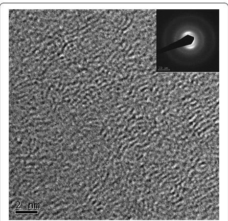
[image:4.595.59.539.553.701.2]Figure 2HRTEM images and the respective diffraction pattern (inset) of carbon films.Deposited at 300 V and irradiated by a 462.5-mJ/cm2laser.
Authors’contributions
MS and EHTT contributed on performing the experiments and writing the paper. Professor TBK contributed as the scientific advisor of the project upon performing the experiments. All authors read and approved the final manuscript.
Authors’information
MS is currently working as a research scientist in the Data Storage Institute (DSI). He is studying the mechanical electrical and thermal properties of carbon thin films and nanostructures. EHTT is working as NTU-DSO postdoc fellow studying electrical mechanical and thermal properties of
nanomaterials. TBK is a professor in the School of Electrical and Electronic Engineering, NTU. His team is working on the synthesis, characterization, and applications of nanomaterials and thin films.
Received: 29 November 2011 Accepted: 1 June 2012 Published: 1 June 2012
References
1. Carey JD, Forrest RD, Khan RUA, Silva SRP:Influence of sp2 clusters on the field emission properties of amorphous carbon thin films.Appl Phys Lett
2000,77:2006–2008.
2. Carey JD, Forrest RD, Silva SRP:Origin of electric field enhancement in field emission from amorphous carbon thin films.Appl Phys Lett2001, 78:2339–2341.
3. Forrest RD, Burden AP, Silva SRP, Cheah LK, Shi X:A study of electron field emission as a function of film thickness from amorphous carbon films.
Appl Phys Lett1998,73:3784–3786.
4. Hart A, Satyanarayana BS, Milne WI, Robertson J:Field emission from tetrahedral amorphous carbon as a function of surface treatment and substrate material.Appl Phys Lett1999,74:1594.
5. Ilie A, Ferrari AC, Yagi T, Robertson J:Effect of sp2-phase nanostructure on field emission from amorphous carbons.Appl Phys Lett2000,76:2627. 6. Ilie A, Hart A, Flewitt AJ, Robertson J, Milne WI:Effect of work function and
surface microstructure on field emission of tetrahedral amorphous carbon.J Appl Phys2000,88:6002–6010.
7. Satyanarayana BS, Hart A, Milne WI, Robertson J:Field emission from tetrahedral amorphous carbon.Appl Phys Lett1997,71:1430. 8. Robertson J:Diamond-like amorphous carbon.Materials Science and
Engineering: R: Reports2002,37:129–281.
9. Chaumet PC, Dufour JP:Electric potential and field between two different spheres.J Electrost1998,43:145–159.
10. Amaratunga GAJ, Silva SRP:Nitrogen containing hydrogenated amorphous carbon for thin-film field emission cathodes.Applied Physics Letters1996,68:2529–2531.
11. Zhao JP, Chen ZY, Wang X, Shi TS, Yano T:Thickness-independent electron field emission from tetrahedral amorphous carbon films.Appl Phys Lett2000,76:191–193.
12. McKenzie DR, Bilek MMM:Thermodynamic theory for preferred orientation in materials prepared by energetic condensation.Thin Solid Films2001,382:280–287.
13. Shakerzadeh M, Teo EHT, Sorkin A, Bosman M, Tay BK, Su H:Plasma density induced formation of nanocrystals in physical vapor deposited carbon films.Carbon2011,49:1733–1744.
14. Lau DWM, Moafi A, Taylor MB, Partridge JG, McCulloch DG, Powles RC, McKenzie DR:The structural phases of non-crystalline carbon prepared by physical vapour deposition.Carbon2009,47:3263–3270.
15. Teo EHT, Bolker A, Kalish R, Saguy C:Nano-patterning of through-film conductivity in anisotropic amorphous carbon induced using conductive atomic force microscopy.Carbon2011,49:2679–2682.
16. Shakerzadeh M, Xu N, Bosman M, Tay BK, Wang X, Teo EHT, Zheng H, Yu H: Field emission enhancement and microstructural changes of carbon films by single pulse laser irradiation.Carbon2011,49:1018–1024. 17. Tan CW, Maziar S, Teo EHT, Tay BK:Microstructure and through-film
electrical characteristics of vertically aligned amorphous carbon films.
Diamond Relat Mater2011,20:290–293.
18. Shakerzadeh M, Samani MK, Khosravian N, Teo EHT, Bosman M, Tay BK: Thermal conductivity of nanocrystalline carbon films studied by pulsed photothermal reflectance.Carbon2012,50:1428–1431.
19. Tay BK, Zhao ZW, Chua DHC:Review of metal oxide films deposited by filtered cathodic vacuum arc technique.Materials Science and Engineering: R: Reports2006,52:1–48.
20. Ferrari AC, Libassi A, Tanner BK, Stolojan V, Yuan J, Brown LM, Ridil SE, Kleinsorge B, Robertson J:Density, sp3 fraction, and cross-sectional structure of amorphous carbon films determined by X-ray reflectivity and electron energy-loss spectroscopy.Phys Rev B: Condens Matter2000, 62:11089–11103.
doi:10.1186/1556-276X-7-286
Cite this article as:Shakerzadehet al.:Thickness dependency of field
emission in amorphous and nanostructured carbon thin films.Nanoscale
Research Letters20127:286.
Submit your manuscript to a
journal and benefi t from:
7Convenient online submission 7Rigorous peer review
7Immediate publication on acceptance 7Open access: articles freely available online 7High visibility within the fi eld
7Retaining the copyright to your article