© 2016, IRJET | Impact Factor value: 4.45 | ISO 9001:2008 Certified Journal
| Page 700
Comparative Analysis of Different Space Vector Switching Scheme for
Five-Phase Voltage Source Inverter
G.RENUKA DEVI
1, V.AYYAPPAN
21
Department of Electrical & Electronics Engineering,
Manakula Vinayagar Institute of Technology, Puducherry-605 107, India
2
Hitec Solutions & Services, Puducherry-605 009, India
Email: [email protected]
---***---Abstract -
This paper presents the comparative analysis ofthree different SVPWM methods for a five-phase voltage source inverter (VSI) in matlab/simulink. Five-phase voltage source inverters are dominantly used to supply the five-phase drives which are used for high power applications. It is necessary to develop appropriate space vectors for the inverters to provide required output voltages to a five phase machine. In the SVPWM technique a large, medium and combinations of large and medium space vectors are detailed. The performances of the inverter with 5-phase are analyzed with these switching techniques. The output voltage, THD and lower order harmonics are observed through simulation. The performances of the inverter with the above switching vectors are compared for different modulation indices and the results are presented.
Key Words: Large space vectors, medium space vectors, large and medium space vectors, SVPWM, voltage source inverters.
1. INTRODUCTION
Multi-phase (phase order more than three) machine drives are gaining growing attention in recent years, due to their several inherent benefits such as reduced torque pulsation, harmonic content, current per phase without increasing the voltage per phase, higher reliability and increased power in the same frame as compared to their three phase counterpart. Multi-phase inverter fed induction motor drives has been found to be quite capable for high power ratings and other specific applications are extensively analyzed in [1-3]. These multiphase load requires a multiphase inverter as source for these loads. An inverter circuit topology uses two switches connected in series as one inverter pole. The number of inverter poles depends on number of phases. For example, a three-phase inverter will have three inverter poles whereas a five-phase inverter circuit will have five inverter poles. Therefore, appropriate PWM methods are necessary for five-phase inverters. A number of PWM techniques are available to control a two-level three-phase VSI. However, SVPWM has become the most popular one because of the easiness of digital implementation and better DC bus utilisation compared to sinusoidal PWM method. SVPWM for three-phase voltage source inverter has been extensively discussed in the literature [4]. The similar
© 2016, IRJET | Impact Factor value: 4.45 | ISO 9001:2008 Certified Journal
| Page 701
However, this situation can only be maintained up to acertain value of the input reference, which is considerably smaller than the maximum reference achievable with the given DC link voltage. In order to enable full utilisation of the available DC bus voltage, the scheme is further complemented with a different SVPWM method proposed [20-22], which enables smooth transition from application of four active vectors to application of only two vectors. To achieve full utilisation of the DC bus, ultimately has to go back to application of large vectors only. In this paper, a novel SVPWM strategy of five-phase VSI is developed. Five-phase voltage source inverters are dominantly used to supply the five-phase drives which are used for high power applications. It is necessary to develop appropriate space vectors for the inverters to provide required output voltages to a five phase machine. In the SVPWM technique a large, medium and combinations of large and medium space vectors are detailed. An attempt is made in this paper for various simulation results are obtained for five-phase inverter at different modulation indices. The effectiveness of this method is investigated based on the concept of full utilisation of the DC bus voltage, THD and low order harmonics for different active space vector combinations.
2. FIVE-PHASE VOLTAGE SOURCE INVERTER
The five-phase voltage source inverter power circuit is shown in Fig. 1. The inverter input DC voltage is considered promote on constant. The load is taken as star-connected and the inverter output phase voltages are denoted with lower case symbols (a,b,c,d,e), while the leg voltages have symbols in capital letters (A,B,C,D,E). The relationship between the machine's phase-to-neutral voltages and inverter leg voltages is given as follows
4 1 ( ) 5 5 4 1 ( ) 5 5 4 1 ( ) 5 5 4 1 ( ) 5 5 4 1 ( ) 5 5
a A B C D E F
b B A C D E F
c C A B D E F
d D a b c E F
e E A B C D F
V V V V V V V
V V V V V V V
V V V V V V V
V V V V V V V
V V V V V V V
(1)
During the operation of a SVPWM method for five-phase VSI as 25 = 32 possible switching configurations with 30 active
vectors and 2 zero vectors. A universal option is to use utilization level of the available DC bus voltage through the definition of the modulation index (M). Since analysis is here restricted only to the linear modulation region, modulation index is defined as the ratio of the fundamental component amplitude of the line-to-neutral inverter output voltage to one half of the available DC bus voltage.
0.5 dc
v M
v
(2)
3. SVPWM FOR FIVE-PHASE VSI
Decoupling transformation matrix for a five-phase system is given with:
1 cos cos 2 cos 3 cos 4
0 cos 2 cos 4 cos cos 3
2
1 sin sin 2 sin 3 sin 4
5
0 sin 2 sin 4 sin sin 3
1 1 1 1 1
2 2 2 2 2
c (3)
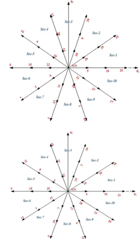
By applying (3) to the phase-to-neutral voltages of a five phase load (1), one obtains space vectors in the d1q1and
2 2
d q planes, Fig. 2. There are 32 space vectors in each
plane (30 active and 2 zero space vectors) and each space vector corresponds to one switching configuration. Space vectors are identified with decimal numbers in Fig.2. By converting each decimal number into a five-digit binary number, switching functions that define particular space vector are obtained. The most significant bit (MSB) of the binary number matches the value of the switching function
Va, the second MSB that of Vb, etc. Active space vectors can be classified into three different groups in accordance with their magnitudes that are termed short, medium and large space vectors. The magnitude of the short, medium and large space vectors are
© 2016, IRJET | Impact Factor value: 4.45 | ISO 9001:2008 Certified Journal
| Page 702
4
cos(2 / 5) 5
2 5 4
cos( / 5) 5
s dc
m dc
l dc
V V
V V
V V
(4)
Thus d1q1 and d2q2 planes can be visualized as being
composed of three different decagons, which are formed by these vector groups, and at the same time, each plane can be divided into 10 sectors (each spanning / 5). Important
benefit obtained with this vector space decomposition is decoupled harmonic mapping into two planes, since harmonics of the order 10k ±1 (k = 0,1,2,3…). Appear only in the d1q1 plane, while d2q2plane contains harmonics of
the order 10k ±3. Harmonic components of the order 5k that would normally appear as zero sequence components cannot exist due to the star connection of the load. Therefore, in order to generate pure sinusoidal output voltages, SVPWM technique must synthesize fundamental component in the
1 1
d q plane, while simultaneously keeping harmonic
components in the d2q2plane at zero average value. A
space vector PWM method, based on utilization of only two large active space vectors (2L), is considered first. This is the simplest extension of a three-phase SVPWM and only the first plane is considered in order to generate output voltages, based on the reference space vector. By using the same concept utilization in the medium space vectors of only two medium active space vectors (2M) for second plane is considered. Next, the number of active space vectors involved in the switching pattern is increased to four (2L and 2M). Nominal set of appropriate mathematical expressions are necessary to implement the three types of techniques are detailed in the following subsections.
3.
1
SVPWM USING LARGE SPACE VECTORS
In this section, the outer-most decagon of large space vectors in d1–q1 plane is considered. The input reference voltage vector is synthesised from two active vectors and zero space vectors respectively. The switching times are calculated by using the reference space vector Vref, magnitude of thelarger plane andsector (sec) number respectively. The switching time sequence of active and zero space voltage vectors is derived from the expressions (5) & (6).
[image:3.595.315.543.347.735.2](5)
Fig.3 shows the phasor diagram for large space vectors of five-phase VSI. Here, tal and tbl correspond to times of application of large space vectors. In sector 1, talis the time of application of the voltage space vector V25, while tblis the time of application of the voltage space vector V24. t0and t31 is the time of application of zero voltage vectors of V0 and
V31. For odd sectors, the sequence of the switching period is
(t0 tbl tal t31 t31 tal tbl t0), while in even sectors it is (t0 tal tbl t31
t31 tbl tal t0) respectively. The maximum possible fundamental peak voltage of large space vector isVmaxVlcos( /10) Vdc0.6155Vdc. The switching time sequence for
large space vectors of sector 1 is shown in Fig.4. It is seen that in one complete full cycle (ts) has divided into two half cycles (ts/2). In the first half of the switching time sequence is zero space vector (t0), two active space vectors (tbl tal ) and zero space vector (t31) respectively. The second half of the switching time sequence is a mirror image of the first cycle.
Fig -2: d1-q1 and d2-q2 planes for five-phase VSI
0 0.5(s al bl)
t t t t
(6)
sin(sec / 5 )
sin / 5
sin( (sec 1) / 5)
sin / 5
ref
al s
l ref
bl s
l
V
t t
V V
t t
V
© 2016, IRJET | Impact Factor value: 4.45 | ISO 9001:2008 Certified Journal
| Page 703
Fig-3: Phasor diagram for
large space vectors
(sector 1)
Fig-4: Switching time
sequence of large space
vectors (sector 1)
3.2 SVPWM USING MEDIUM SPACE VECTORS
In this section, the medium decagon of space vectors in d1 –
q1 plane is considered. The input reference voltage vector is synthesised from two active vectors and zero space vectors. The switching time is calculated by using the reference space vector Vref, magnitude of themedium plane andsector (sec) number respectively. The switching time sequence of active and zero space voltage vectors is derived from the expressions (7) & (8).
sin(sec / 5 ) sin / 5 sin( (sec 1) / 5)
sin / 5 ref
am s
m
ref
bm s
m V
t t
V
V
t t
V
(7)
0 0.5(s am bm)
t t t t (8)
where ts =1/fs
ts- Sampling time
fs- Sampling frequency equal to carrier frequency.
Fig.5 shows the phasor diagram for medium space vectors of five-phase VSI. Here, tam and tbm correspond to times of application of medium space vectors. Thus, in sector 1, tamis the time of application of the voltage space vector V16, while tbmis the time of application of the voltage space vector V29. t0and t31 is the time of application of zero voltage vectors of
V0 and V31 respectively. For odd sectors, the sequence of the switching period is (t0 tam tbm t31 t31 tbm tam t0), while in even sectors it is (t0 tbm tam t31 t31 tam tbm t0). The maximum possible fundamental peak voltage of medium space vector isVmaxVmcos( /10) Vdc0.3804Vdc. The switching time sequence for
medium space vectors of sector 1 is shown in Fig.6. It is seen that in one complete full cycle (ts) has divided into two half cycles (ts/2). In the first half of the switching time sequence is zero space vector (t0), two active space vectors (tam tbm)
and zero space vector (t31) respectively. The second half of the switching time sequence is a mirror image of the first cycle.
Fig-5 Phasor diagram of medium space vector (sector 1)
Fig-6: Switching time sequence of medium space vector (sector 1)
3.3 SVPWM USING LARGE AND MEDIUM SPACE
VECTORS
In this section, the outer and medium decagon of space vectors in d1-q1 plane is considered. The input reference voltage vector is synthesised from four active and zero space vectors respectively. The switching times are calculated using the reference space vector Vref, magnitude of thelarge and medium plane andsector (sec) number respectively. The switching time sequence of active and zero voltage vectors is derived from the expressions (9) to (12).
a al am
b bl bm
t
t
t
t
t
t
(9)s m
al am
s m
bl bm
t V
t
V
t V
t
V
(10)Solving the expression (10) & (11), switching times for
active space vectors are obtained as
:
:
l l
al a bl b
l m l m
m m
am a bm b
l m l m
V
V
t
t
t
t
V
V
V
V
V
V
t
t
t
t
V
V
V
V
© 2016, IRJET | Impact Factor value: 4.45 | ISO 9001:2008 Certified Journal
| Page 704
0
0.5(
s al bl am bm)
t
t t
t
t
t
(12)Fig.7 shows the phasor diagram for combinations of large and medium space vectors of five-phase VSI. Here, taland tbl correspond to times of application of active large space vectors and tamand tbmcorrespond to times of application of active medium space vectors. t0 and t31 are the time of application of zero voltage vectors of V0 and V31 respectively. In the combinations of large and medium space vectors the sequence of odd sectors is (t0tam tbl tal tbm t31t31tbm tal tbl tam
t0), while in even sectors it is (t0tbm tal tbl tam t31 t31tam tbl tal
tbm t0). The maximum possible fundamental peak voltage of
combinations of large and medium space vector isVmcos( /10) VdcVmaxVlcos( /10) Vdc. The switching time
sequence with combinations of large and medium space vectors of sector 1 is shown in Fig. 8. It is seen that in one complete full cycle (ts) has divided into two half cycles (ts/2). In the first half of the switching time sequence is zero space vector (t0), four active space vectors (tam tbl tal tbm) and zero space vector (t31) respectively. The second half of the switching time sequence is a mirror image of the first cycle.
Fig-7: Phasor diagram for combinations of large and medium space vector (sector 1)
Fig-8: Switching time sequence with combinations of large and medium space vector (sector 1)
4. SIMULATION RESULTS
A simulation is performed in order to prove the efficiency of the schemes are compared in terms of dc bus utilization, THD and lower order harmonic components of output phase voltages. In the simulation the dc link voltage is set to 1 p.u. and the modulation index Mis varying from 0.2 to 1. The switching frequency of the VSI is chosen as 10 kHz and the reference fundamental frequency is kept equal to 50 Hz. In the simulation the results are presented for large, medium and large and medium space vectors for 5-phase VSI.Fig.9 shows the resultant SVPWM signal for large space vectors. Fig.10 shows the SVPWM results of phase voltage and its spectrum of large space vector of 5-phase VSI. From the observation the fundamental rms value equals 0.4434p.u.
(0.627p.u.peak) and THD is 46.91%. In the large space vectors the maximum DC bus utilization is 85.64%. The medium space vector modulating signals and fundamental is shown in Fig.11 and 12. It is seen that the fundamental rms value equals 0.2766p.u. (0.3912p.u.peak) and THD is 104.42% of medium space vectors. The large and medium space vector modulating signals and fundamental is shown in Fig.13 and 14. It is seen that the fundamental rms value equals 0.3862p.u. (0.5462p.u.peak) and THD is 65.46% of large and medium space vectors. In the large and medium space vectors the fundamental voltage is lies between
max
0.3804Vdc V 0.6155Vdc. It is seen from Fig.15 that the
decrease of THD for different space vectors when increasing modulation indices. Fig.16 shows the maximum fundamental voltage of different space vectors for under varying modulation indices. It is seen that minimum THD and maximum fundamental voltage observed in the large space vector combinations. Fig.17&18 shows the lower order harmonics of the 3rd and 7th harmonics. It is seen that
minimum harmonics found in the large and medium space vectors.
Fig-9: Resultant modulating signal for large space vectors
© 2016, IRJET | Impact Factor value: 4.45 | ISO 9001:2008 Certified Journal
| Page 705
Fig-11: Resultant modulating signal for medium space vectors
Fig-12: SVPWM results of medium space vectors output phase voltage and its spectrum for M= 0.85
Fig-13: Resultant modulating signal for large and medium space vectors
Fig-14: SVPWM results of large and medium space vectors output phase voltage and its spectrum for M= 0.85
Fig-15: Percentage decrease of THD for different space vectors
Fig-16: Fundamental voltage increase for different space vectors combinations
Fig-17: 3rd harmonic for
different space vectors Fig-18: 7
th harmonic for
different space vectors
5. CONCLUSION
© 2016, IRJET | Impact Factor value: 4.45 | ISO 9001:2008 Certified Journal
| Page 706
switching scheme. The THD decreases with increasingmodulation index and it is minimum for large space vectors. However the lower order harmonics are minimum in the large and medium space vectors. The maximum DC bus utilization is observed in the large space vectors combinations. Based on the THD, DC bus utilization and switching pattern and space vector disposition complexity in the large space vectors are optimum for the five-phase voltage source inverters.
REFERENCES
[1] G.K.Singh,“Multi-phase induction machine drive research – a survey,electric Power System Research, vol. 61, pp. 139-147,2002.
[2] G.Renukadevi and K.Rajambal, “Generalized Model of Multi-Phase Induction Motor Drive using Matlab/Simulink,” International IEEE PES Conference Innovative Smart Grid Technologies,Kerala-India, 2011. [3] E.Levi,R.Bojoi,F.Profumo,H.A.Toliyat and S. williamson, “Multiphase induction motor drives-A technology status review”,IET Elect. Power Appl. vol. 1, no. 4, pp. 489-516, July 2007.
[4] G.D.Holmes, T.A.Lipo, “Pulse Width Modulation for Power
Converters -Principles and Practice,” IEEE Press Series on Power Engineering, John Wiley and Sons, Piscataway, NJ, USA, 2003.
[5] Y.Zhao, T.A.Lipo. Space vector PWM control of dual three-phase induction machine using vector space decomposition, IEEE Trans. on Industry Applications, vol. 31, no. 5, 1995, pp. 1 100-1 109.
[6] R.O.C.Lyra, T.A.Lipo, “Torque density improvement in a sixphase induction motor with third harmonic current injection,”IEEE Trans. on Industry Applications, vol. 38, no. 5, 2002, pp.1351-1360.
[7] H.M.Ryu, J.H.Kim, S.K.Sul, “Analysis of multi-phase space vector pulse width modulation based on multiple d-q spaces concept,” IEEE Trans. on Power Electronics, vol. 20, no. 6, 2005, 1364-1371.
[8] S. Xue, X. Wen, Z. Feng, “A novel multi-dimensional SVPWM strategy of multiphase motor drives,” Proc. Power Electronics and Motion Control Conf. EPE-PEMC,
pp. 931-935, 2006.
[9] E.Levi, “Multiphase Electric Machines for Variable Speed Applications,” IEEE Transactions on Industrial Electronics, vol. 55, no. 5, pp. 1893-1909, MAY 2008. [10] A.Iqbal, E.Levi, M.Jones, S.N.Vukosavic, “Generalised
sinusoidal PWM with harmonic injection for multi-phase VSIs,” Proc. IEEE Power Elec. Spec. Conf., PESC,
Jeju, Korea, 2006, pp. 2871-2877.
[11] D.Casadei, G.Serra, A.Tani, L.Zarri, “Multi-phase inverter modulation strategies based on duty-cycle space vector approach,”Proc. of Ship Propulsion and Railway Systems Conf. SPRTS,Bologna, Italy, 2005, pp. 222-229.
[12] G.Renukadevi and K.Rajambal, “Novel Carrier-Based PWM technique for n-Phase VSI,” International Journal of Energy Technologies and Policy, 2011, pp. 1-9. [13] O.Ojo, G.Dong, “Generalized discontinuous carrier-based
PWM modulation scheme for multi-phase converter-machine systems,” Proc. IEEE Ind. Appl. Soc. Annual Meeting IAS, Hong Kong,2005, CD-ROM paper IAS38p3. [14] Joohn-Sheok Kim and Seung-Ki Sul, “A novel voltage modulation technique of the space vector PWM”, in Conf. Rec. IPEC’95, Yokohama, Japan, 1995, pp. 742-747. [15] T.Brahmananda Reddy, J. Amarnath and D.
Subbarayudu,“Improvement of DTC performance by using hybrid space vector Pulsewidth modulation algorithm” International Review of Electrical Engineering, Vol.4, no.2, pp. 593-600,Jul-Aug, 2007. [16] Kelly, J.W., Strangas, E.G., and Miller, J.M.: ‘Multi-phase
inverter analysis’. Proc. IEEE Int. Electric Machines and Drives Conf. IEMDC, Cambridge, MA, 2001, pp. 147– 155.
[17] R.Shi, H.A.Toliyat, “Vector control of five-phase synchronous reluctance motor with space vector pulse width modulation (SVPWM) for minimum switching losses,” Proc. IEEE Applied Power Elec. Conf. APEC, Dallas, Texas, 2002, pp. 57-63.
[18] H.A.Toliyat, R.Shi, H.Xu, “DSP-based vector control of five-phase synchronous reluctance motor,” IEEE Industry Applications Society Annual Meeting IAS, Rome, Italy, 2000, CD-ROM paper no. 40_05.
[19] P.S.N.deSilva, J.E.Fletcher, B.W.Williams, “Development of space vector modulation strategies for five-phase voltage source inverters,” Proc. IEE Power Electronics, Machines and Drives Conf. PEMD, Edinburgh, UK, 2004, pp. 650-655.
[20] Iqbal and S. Moinuddin, “Space vector model of a five-phase voltage source inverter,” in Proc. IEEE Int. Conf. Ind. Technol. (ICIT 2006), Mumbai, India, Dec.15–17, pp. 488–493, Paper IF 002909 [CD-ROM].
[21] A.Iqbal, E.Levi, “Space vector modulation scheme for a five-phase voltage source inverter,” Proc. European Power Electronics (EPE) Conf., Dresden, Germany, 2005, CD-ROM paper no. 0006.pdf.
[22] A.Iqbal, E.Levi, “Space vector PWM techniques for sinusoidal output voltage generation with a five-phase voltage source inverter,” Electric Power Components and Systems, 2006, vol. 34 no. 2.